DE102010013286B4 - LED lamp for homogeneous illumination of hollow bodies - Google Patents
LED lamp for homogeneous illumination of hollow bodies Download PDFInfo
- Publication number
- DE102010013286B4 DE102010013286B4 DE102010013286A DE102010013286A DE102010013286B4 DE 102010013286 B4 DE102010013286 B4 DE 102010013286B4 DE 102010013286 A DE102010013286 A DE 102010013286A DE 102010013286 A DE102010013286 A DE 102010013286A DE 102010013286 B4 DE102010013286 B4 DE 102010013286B4
- Authority
- DE
- Germany
- Prior art keywords
- chip
- lighting device
- board led
- leds
- led module
- Prior art date
- Legal status (The legal status is an assumption and is not a legal conclusion. Google has not performed a legal analysis and makes no representation as to the accuracy of the status listed.)
- Active
Links
- 238000005286 illumination Methods 0.000 title description 21
- 239000000463 material Substances 0.000 claims description 21
- 238000001816 cooling Methods 0.000 claims description 18
- 230000003287 optical effect Effects 0.000 claims description 8
- 238000004382 potting Methods 0.000 claims description 8
- 238000001035 drying Methods 0.000 claims description 4
- 238000003384 imaging method Methods 0.000 claims description 4
- 230000001788 irregular Effects 0.000 claims description 4
- 239000000853 adhesive Substances 0.000 claims description 3
- 230000001070 adhesive effect Effects 0.000 claims description 3
- 230000007423 decrease Effects 0.000 claims description 3
- 239000003973 paint Substances 0.000 claims description 3
- 239000011347 resin Substances 0.000 claims description 3
- 229920005989 resin Polymers 0.000 claims description 3
- 230000005611 electricity Effects 0.000 claims 1
- 239000000758 substrate Substances 0.000 description 41
- 238000005516 engineering process Methods 0.000 description 32
- 230000005855 radiation Effects 0.000 description 20
- 238000009826 distribution Methods 0.000 description 11
- 238000000034 method Methods 0.000 description 10
- 239000004020 conductor Substances 0.000 description 9
- 239000011521 glass Substances 0.000 description 9
- 238000001723 curing Methods 0.000 description 8
- 239000007789 gas Substances 0.000 description 7
- 239000011248 coating agent Substances 0.000 description 6
- 238000000576 coating method Methods 0.000 description 6
- 239000002184 metal Substances 0.000 description 6
- 229910052751 metal Inorganic materials 0.000 description 6
- 238000010276 construction Methods 0.000 description 5
- 238000005457 optimization Methods 0.000 description 5
- 230000001681 protective effect Effects 0.000 description 5
- XLYOFNOQVPJJNP-UHFFFAOYSA-N water Substances O XLYOFNOQVPJJNP-UHFFFAOYSA-N 0.000 description 5
- 238000003848 UV Light-Curing Methods 0.000 description 4
- 230000006978 adaptation Effects 0.000 description 4
- 238000005259 measurement Methods 0.000 description 4
- 238000011161 development Methods 0.000 description 3
- 239000007788 liquid Substances 0.000 description 3
- 230000007246 mechanism Effects 0.000 description 3
- 229920001296 polysiloxane Polymers 0.000 description 3
- 230000002829 reductive effect Effects 0.000 description 3
- 230000003595 spectral effect Effects 0.000 description 3
- 238000003491 array Methods 0.000 description 2
- 239000000919 ceramic Substances 0.000 description 2
- 238000010586 diagram Methods 0.000 description 2
- 238000011049 filling Methods 0.000 description 2
- 238000012423 maintenance Methods 0.000 description 2
- 238000004519 manufacturing process Methods 0.000 description 2
- 238000012856 packing Methods 0.000 description 2
- 239000004033 plastic Substances 0.000 description 2
- 229920003023 plastic Polymers 0.000 description 2
- 230000035939 shock Effects 0.000 description 2
- 238000005476 soldering Methods 0.000 description 2
- 239000000126 substance Substances 0.000 description 2
- 239000012780 transparent material Substances 0.000 description 2
- NIXOWILDQLNWCW-UHFFFAOYSA-M Acrylate Chemical compound [O-]C(=O)C=C NIXOWILDQLNWCW-UHFFFAOYSA-M 0.000 description 1
- 239000004593 Epoxy Substances 0.000 description 1
- JOYRKODLDBILNP-UHFFFAOYSA-N Ethyl urethane Chemical compound CCOC(N)=O JOYRKODLDBILNP-UHFFFAOYSA-N 0.000 description 1
- VYPSYNLAJGMNEJ-UHFFFAOYSA-N Silicium dioxide Chemical compound O=[Si]=O VYPSYNLAJGMNEJ-UHFFFAOYSA-N 0.000 description 1
- XUIMIQQOPSSXEZ-UHFFFAOYSA-N Silicon Chemical compound [Si] XUIMIQQOPSSXEZ-UHFFFAOYSA-N 0.000 description 1
- 230000001133 acceleration Effects 0.000 description 1
- 238000004026 adhesive bonding Methods 0.000 description 1
- 230000003466 anti-cipated effect Effects 0.000 description 1
- 238000013459 approach Methods 0.000 description 1
- 230000000295 complement effect Effects 0.000 description 1
- 238000010924 continuous production Methods 0.000 description 1
- 230000007797 corrosion Effects 0.000 description 1
- 238000005260 corrosion Methods 0.000 description 1
- 238000005520 cutting process Methods 0.000 description 1
- 238000006731 degradation reaction Methods 0.000 description 1
- 230000001419 dependent effect Effects 0.000 description 1
- 238000013461 design Methods 0.000 description 1
- 239000003651 drinking water Substances 0.000 description 1
- 235000020188 drinking water Nutrition 0.000 description 1
- 239000000428 dust Substances 0.000 description 1
- 238000000295 emission spectrum Methods 0.000 description 1
- 238000005530 etching Methods 0.000 description 1
- 230000005496 eutectics Effects 0.000 description 1
- 230000005284 excitation Effects 0.000 description 1
- 239000004744 fabric Substances 0.000 description 1
- 230000008713 feedback mechanism Effects 0.000 description 1
- 239000005329 float glass Substances 0.000 description 1
- 239000003365 glass fiber Substances 0.000 description 1
- 239000004519 grease Substances 0.000 description 1
- 230000020169 heat generation Effects 0.000 description 1
- 238000000265 homogenisation Methods 0.000 description 1
- 238000007373 indentation Methods 0.000 description 1
- 239000011261 inert gas Substances 0.000 description 1
- 238000009413 insulation Methods 0.000 description 1
- 230000002452 interceptive effect Effects 0.000 description 1
- 230000000670 limiting effect Effects 0.000 description 1
- 150000002739 metals Chemical class 0.000 description 1
- 238000003801 milling Methods 0.000 description 1
- 239000003921 oil Substances 0.000 description 1
- 238000004806 packaging method and process Methods 0.000 description 1
- 230000036961 partial effect Effects 0.000 description 1
- 238000000016 photochemical curing Methods 0.000 description 1
- 239000002985 plastic film Substances 0.000 description 1
- 229920006255 plastic film Polymers 0.000 description 1
- 229920000642 polymer Polymers 0.000 description 1
- 229920002635 polyurethane Polymers 0.000 description 1
- 239000004814 polyurethane Substances 0.000 description 1
- 238000004080 punching Methods 0.000 description 1
- 230000035945 sensitivity Effects 0.000 description 1
- 229910052710 silicon Inorganic materials 0.000 description 1
- 239000010703 silicon Substances 0.000 description 1
- 238000005245 sintering Methods 0.000 description 1
- 238000001228 spectrum Methods 0.000 description 1
- 238000002211 ultraviolet spectrum Methods 0.000 description 1
- 238000009423 ventilation Methods 0.000 description 1
- -1 z. B. borosilicate Substances 0.000 description 1
Images


Classifications
-
- F—MECHANICAL ENGINEERING; LIGHTING; HEATING; WEAPONS; BLASTING
- F21—LIGHTING
- F21K—NON-ELECTRIC LIGHT SOURCES USING LUMINESCENCE; LIGHT SOURCES USING ELECTROCHEMILUMINESCENCE; LIGHT SOURCES USING CHARGES OF COMBUSTIBLE MATERIAL; LIGHT SOURCES USING SEMICONDUCTOR DEVICES AS LIGHT-GENERATING ELEMENTS; LIGHT SOURCES NOT OTHERWISE PROVIDED FOR
- F21K9/00—Light sources using semiconductor devices as light-generating elements, e.g. using light-emitting diodes [LED] or lasers
- F21K9/20—Light sources comprising attachment means
-
- F—MECHANICAL ENGINEERING; LIGHTING; HEATING; WEAPONS; BLASTING
- F21—LIGHTING
- F21K—NON-ELECTRIC LIGHT SOURCES USING LUMINESCENCE; LIGHT SOURCES USING ELECTROCHEMILUMINESCENCE; LIGHT SOURCES USING CHARGES OF COMBUSTIBLE MATERIAL; LIGHT SOURCES USING SEMICONDUCTOR DEVICES AS LIGHT-GENERATING ELEMENTS; LIGHT SOURCES NOT OTHERWISE PROVIDED FOR
- F21K9/00—Light sources using semiconductor devices as light-generating elements, e.g. using light-emitting diodes [LED] or lasers
-
- F—MECHANICAL ENGINEERING; LIGHTING; HEATING; WEAPONS; BLASTING
- F21—LIGHTING
- F21V—FUNCTIONAL FEATURES OR DETAILS OF LIGHTING DEVICES OR SYSTEMS THEREOF; STRUCTURAL COMBINATIONS OF LIGHTING DEVICES WITH OTHER ARTICLES, NOT OTHERWISE PROVIDED FOR
- F21V19/00—Fastening of light sources or lamp holders
- F21V19/001—Fastening of light sources or lamp holders the light sources being semiconductors devices, e.g. LEDs
-
- F—MECHANICAL ENGINEERING; LIGHTING; HEATING; WEAPONS; BLASTING
- F21—LIGHTING
- F21V—FUNCTIONAL FEATURES OR DETAILS OF LIGHTING DEVICES OR SYSTEMS THEREOF; STRUCTURAL COMBINATIONS OF LIGHTING DEVICES WITH OTHER ARTICLES, NOT OTHERWISE PROVIDED FOR
- F21V23/00—Arrangement of electric circuit elements in or on lighting devices
- F21V23/003—Arrangement of electric circuit elements in or on lighting devices the elements being electronics drivers or controllers for operating the light source, e.g. for a LED array
-
- F—MECHANICAL ENGINEERING; LIGHTING; HEATING; WEAPONS; BLASTING
- F21—LIGHTING
- F21V—FUNCTIONAL FEATURES OR DETAILS OF LIGHTING DEVICES OR SYSTEMS THEREOF; STRUCTURAL COMBINATIONS OF LIGHTING DEVICES WITH OTHER ARTICLES, NOT OTHERWISE PROVIDED FOR
- F21V23/00—Arrangement of electric circuit elements in or on lighting devices
- F21V23/04—Arrangement of electric circuit elements in or on lighting devices the elements being switches
-
- F—MECHANICAL ENGINEERING; LIGHTING; HEATING; WEAPONS; BLASTING
- F21—LIGHTING
- F21Y—INDEXING SCHEME ASSOCIATED WITH SUBCLASSES F21K, F21L, F21S and F21V, RELATING TO THE FORM OR THE KIND OF THE LIGHT SOURCES OR OF THE COLOUR OF THE LIGHT EMITTED
- F21Y2107/00—Light sources with three-dimensionally disposed light-generating elements
- F21Y2107/30—Light sources with three-dimensionally disposed light-generating elements on the outer surface of cylindrical surfaces, e.g. rod-shaped supports having a circular or a polygonal cross section
-
- F—MECHANICAL ENGINEERING; LIGHTING; HEATING; WEAPONS; BLASTING
- F21—LIGHTING
- F21Y—INDEXING SCHEME ASSOCIATED WITH SUBCLASSES F21K, F21L, F21S and F21V, RELATING TO THE FORM OR THE KIND OF THE LIGHT SOURCES OR OF THE COLOUR OF THE LIGHT EMITTED
- F21Y2115/00—Light-generating elements of semiconductor light sources
- F21Y2115/10—Light-emitting diodes [LED]
Abstract
Beleuchtungsvorrichtung (40–40'', 45–45'', 50–50'', 60, 80, 93–93''') zum gleichmäßigen Ausleuchten gebogener, nicht ebener oder polyedrischer Flächen, umfassend eine Mehrzahl von ebenen Chip-on-Board-LED-Modulen (1, 11, 11', 21, 31, 41–41'', 46–46'', 51–51'', 61–61'', 71–71''', 811–818), die wenigstens paarweise aneinandergrenzend angeordnet sind, wobei jedes Chip-on-Board-LED-Modul (1, 11, 11', 21, 31, 41–41'', 46–46'', 51–51'', 61–61'', 71– 71''', 811–818) eine Mehrzahl von Licht emittierenden LEDs (4, 4', 14, 14', 24, 34, 64, 72) aufweist, dadurch gekennzeichnet, dass wenigstens ein Paar jeweils benachbarter Chip-on-Board-LED-Module (1, 11, 11', 21, 31, 41–41'', 46–46'', 51–51'', 61–61'', 71–71''', 811–818) bezüglich ihrer Flächennormalen unter einem Winkel angeordnet ist, der größer als 0° ist.Lighting device (40-40 '', 45-45 '', 50-50 '', 60, 80, 93-93 '' ') for uniformly illuminating curved, non-planar or polyhedral surfaces, comprising a plurality of planar chip-on -Board LED modules (1, 11, 11 ', 21, 31, 41-41' ', 46-46' ', 51-51' ', 61-61' ', 71-71' '', 811 818) arranged at least in pairs adjacent each other, each chip-on-board LED module (1, 11, 11 ', 21, 31, 41-41' ', 46-46' ', 51-51' ', 61-61' ', 71-71' '', 811-818) has a plurality of light-emitting LEDs (4, 4 ', 14, 14', 24, 34, 64, 72), characterized in that at least one pair of respectively adjacent chip-on-board LED modules (1, 11, 11 ', 21, 31, 41-41 ", 46-46", 51-51 ", 61-61", 71-71 '", 811-818) is arranged at an angle greater than 0 ° with respect to their surface normal.
Description
Die Erfindung betrifft eine Beleuchtungsvorrichtung zum gleichmäßigen Ausleuchten gebogener, nicht ebener oder polyedrischer Flächen, umfassend eine Mehrzahl von ebenen Chip-on-Board-LED-Modulen, die wenigstens paarweise aneinandergrenzend angeordnet sind, wobei jedes Chip-on-Board-LED-Modul eine Mehrzahl von Licht emittierenden LEDs aufweist. Die Erfindung betrifft ferner eine Beleuchtungseinheit und eine Verwendung.The invention relates to a lighting device for uniform illumination of curved, non-planar or polyhedral surfaces, comprising a plurality of planar chip-on-board LED modules, which are arranged adjacent to each other at least in pairs, wherein each chip-on-board LED module a Comprising a plurality of light emitting LEDs. The invention further relates to a lighting unit and a use.
Ein Anwendungsgebiet, bei dem eine gleichmäßige Ausleuchtung gebogener, polyedrischer oder nicht ebener Flächen notwendig ist, ist die Aushärtung und Belichtung zur Trocknung, Härtung oder Belichtung von Lacken, Klebern, Harzen und weiteren lichtreaktiven Materialien, mit denen die Innenseiten oder Außenseiten von nicht ebenen Körpern beschichtet sind.One area of application in which even illumination of curved, polyhedral or nonplanar surfaces is necessary is curing and exposure for drying, curing or exposure of paints, adhesives, resins and other light reactive materials which cause the insides or outsides of non-planar bodies are coated.
Ein Beispiel hierfür ist die Kanalsanierung, wo es bekannt ist, die Innenseite von Rohren oder Schläuchen mit einer lichthärtbaren Beschichtung oder Substanz in Form eines Schlauches zu versehen. Zum Aushärten eines so genannten „Schlauch-Liners”, eines harzgetränkten Glasfasergewebes mit schützenden Kunststofffolien an den Außenflächen, wird bei einer Kanalsanierung eine Lampe durch den Schlauch oder das Rohr hindurch gezwungen, um das Beschichtungsmaterial abschnittsweise fortschreitend mittels einer intensiven Beleuchtung zu trocknen und auszuhärten. Entsprechende Lampensysteme sind idealerweise bogengängig für Biegungen bis zu 90°. Typische Durchmesser entsprechend beschichteter Rohre und Schläuche sind im Bereich von wenigen Zentimetern bis hin zu mehreren Metern.An example of this is sewer rehabilitation, where it is known to provide the inside of pipes or hoses with a photohardenable coating or substance in the form of a hose. For curing a so-called "hose liner", a resin-impregnated glass fiber fabric with protective plastic films on the outer surfaces, a channel rehabilitation a lamp is forced through the tube or pipe through to progressively dry and cure the coating material in sections by means of intense lighting. Corresponding lamp systems are ideally bendable for bends up to 90 °. Typical diameters of coated tubes and hoses are in the range of a few centimeters to several meters.
Bei diesem Vorgehen ist eine gleichmäßige Belichtung notwendig, um allseitig eine gleichmäßige Trocknung und Härtung des Beschichtungsmaterials zu erreichen. Typische Homogenitätstoleranzen für die Ausleuchtung liegen im Bereich von weniger als ±15% in Bezug auf einen definierten Mittelwert. Die Bestrahlungsstärken auf einer beleuchteten Innenwand betragen für diese Anwendung wenige μW/cm2 bis hin zu 100 W/cm2.In this procedure, a uniform exposure is necessary in order to achieve a uniform drying and curing of the coating material on all sides. Typical homogeneity tolerances for illumination are in the range of less than ± 15% with respect to a defined mean. The irradiances on an illuminated inner wall are for this application a few μW / cm 2 up to 100 W / cm 2 .
Aus der
Um eine hohe Lichtleistung zu erreichen, sind entsprechende bekannte Lampensysteme mit einem Durchmesser versehen, der nur wenige Millimeter unter dem Rohrinnendurchmesser, für den sie ausgelegt sind, liegt. Die Lampe kann sich aber auch bis zu wenigen Metern von der zu bestrahlenden Fläche befinden.In order to achieve a high light output, corresponding known lamp systems are provided with a diameter which is only a few millimeters below the pipe inside diameter for which they are designed. The lamp can also be up to a few meters from the surface to be irradiated.
Ähnliche Anforderungen sind zur Innenausleuchtung weiterer radiärsymmetrischer konvexer Hohlkörper bekannt. Dies trifft etwa im Bereich der Beleuchtungstechnik zu, z. B. für architektonisches Licht, für die UV-Härtung und Belichtung langer Körper oder von Hohlräumen mit bestimmter Querschnittsgeometrie. Entsprechende Geometrien sind beispielsweise Rohre, Kegel, Kugeln, polyedrische Körper oder ähnliche.Similar requirements are known for the interior illumination of other radiärsymmetrischer convex hollow body. This is true for example in the field of lighting technology, z. As for architectural light, for UV curing and exposure of long body or cavities with certain cross-sectional geometry. Corresponding geometries are, for example, tubes, cones, spheres, polyhedral bodies or the like.
Für das Anwendungsbeispiel der lichthärtenden Kanalsanierung werden bislang meistens Gasentladungslampen eingesetzt, die eine intensive Lichtabgabe bereitstellen. Die traditionell verwendeten Lampen auf Gasentladungsbasis entwickeln eine starke Wärmestrahlung bzw. Infrarotstrahlung, die bei zu dichter Annäherung der Lampe an das zu beleuchtende Objekt bzw. bei zu langanhaltender Bestrahlung das Objekt und die auszuhärtende Beschichtung aufheizt. Für UV-Härtungsprozesse bedeutet dies, dass die zu vernetzenden Polymere dissoziieren können. In der Kanalsanierung kann so das zu härtende Liner-Material thermisch geschädigt werden.For the application example of light-curing sewer rehabilitation so far mostly gas discharge lamps are used, which provide an intense light output. The traditionally used gas discharge lamps develop a strong heat radiation or infrared radiation, which heats up the object and the coating to be cured if the lamp approaches the object to be illuminated too tightly or if the irradiation is too long. For UV curing processes, this means that the polymers to be crosslinked can dissociate. In the sewer rehabilitation, the liner material to be hardened can thus be thermally damaged.
Die bekannten Lampen sind vor allem für größere Rohrdurchmesser geeignet, aufgrund ihrer Baugröße allerdings weniger für kleinere Rohrdurchmesser, wie sie zum Beispiel im Hausanschlussbereich vorkommen, mit typischen Rohrdurchmessern entsprechend 160 mm Nenndurchmesser oder kleiner. Hierfür sind keine Gasentladungslampensysteme verfügbar, die durch Bögen mit 45°-Winkeln oder 90°-Winkeln schleppbar sind.The known lamps are particularly suitable for larger pipe diameters, but due to their size less for smaller pipe diameters, as they occur, for example, in the service area, with typical pipe diameters corresponding to 160 mm nominal diameter or smaller. For this purpose, no gas discharge lamp systems are available, which can be towed by arcs with 45 ° angles or 90 ° angles.
Zu kleinen Baugrößen hin ist die traditionelle UV-Lampentechnologie durch die erreichbare Mindestgröße der Lampen begrenzt. Eine weitere Einschränkung in dieser Beziehung besteht auch aufgrund der Notwendigkeit einer mechanisch robusten Halterung und Schutzvorrichtung für die Lampen, die in der Regel aus einem mit einer Substanz gefüllten Glashüllkörper bestehen, in dem die Gasentladung zwischen zwei gegenüberliegenden Elektroden oder durch eine elektrodenlose Anregung mit Mikrowellen stattfindet. Bei einer entsprechenden mechanisch robusten Halterung oder Schutzvorrichtung, beispielsweise in Form von die Lampe umgebenden Metallstäben, sind Abschattungen der emittierten Strahlung in Kauf zu nehmen. Diese Inhomogenitäten der Abstrahlung sind nachteilig, wenn eine gleichmäßige Bestrahlung erforderlich ist, wie beispielsweise in der UV-Härtung.For small sizes, the traditional UV lamp technology is limited by the achievable minimum size of the lamps. Another limitation in this regard is also due to the need for a mechanically robust support and protection for the lamps, which are typically a glass filled body filled with a substance, in which the gas discharge takes place between two opposing electrodes or by electrodeless excitation with microwaves , With a corresponding mechanically robust holder or protective device, for example in the form of metal rods surrounding the lamp, shadowing of the emitted radiation is to be accepted. These inhomogeneities of radiation are disadvantageous when uniform irradiation is required, such as in UV curing.
Insbesondere die Nutzung mehrerer traditioneller Glaskolben-Lampen zur Erreichung hoher Bestrahlungsstärken erschwert das Erreichen einer homogenen Beleuchtung aufgrund der deutlichen geometrischen Ausdehnung dieser Lampen, wenn diese in Umfangsrichtung, beisplelsweise eines Rohres, nebenelnander angeordnet sind. Dies resultiert daraus, dass erst in einem geometrischen Abstand, der dem Abstand der Emissionszentren entspricht, ein guter Überlauf der emittierten Strahlungsfelder stattfindet, so dass Einbrüche der Bestrahlungsstärke durch die fehlende Emission zwischen den Emissionszentren der Lampen zu starken Inhomogenitäten in Umfangsrichtung führen. in diesem Fall müssen evtl. aufwändige Optiken zur Homogenisierung der Beleuchtung eingesetzt werden.In particular, the use of several traditional glass bulb lamps to achieve high irradiance levels makes it difficult to achieve a homogeneous illumination due to the significant geometric extension of these lamps, if this in the circumferential direction, beisplelsweise one Pipe, nebenelnander are arranged. This results from the fact that only at a geometric distance corresponding to the distance of the emission centers, a good overflow of the emitted radiation fields takes place, so that falls in the irradiance by the lack of emission between the emission centers of the lamps lead to strong inhomogeneities in the circumferential direction. in this case possibly complex optics must be used to homogenize the lighting.
Der vorliegenden Erfindung liegt daher die Aufgabe zugrunde, eine Beleuchtungsvorrichtung zum gleichmäßigen Ausleuchten gebogener, nicht ebener oder polyedrischer Flächen zur Verfügung zu stellen, die für kompakte Hohlkörper bzw. Körper von typischen Innendurchmessern bzw. Außendurchmessern im Bereich von wenigen Millimetern bis hin zu mehreren Metern anwendbar sind und Bestrahlungsstärken auf der beleuchteten Innen- bzw. Außenwandung im Bereich von einigen 10 μW/cm2 bis hin zu 100 W/cm2 ermöglichen. Die Beleuchtungsvorrichtung soll insbesondere für die Kanalsanierung verwendbar sein.The present invention is therefore based on the object to provide a lighting device for uniform illumination curved, non-planar or polyhedral surfaces available for compact hollow body or body of typical inner diameters or outer diameters in the range of a few millimeters up to several meters and irradiances on the illuminated inner or outer wall in the range of some 10 μW / cm 2 to 100 W / cm 2 allow. The lighting device should be usable in particular for the sewer rehabilitation.
Diese Aufgabe wird gelöst durch eine Beleuchtungsvorrichtung zum gleichmäßigen Ausleuchten gebogener, nicht ebener oder polyedrischer Flächen, umfassend eine Mehrzahl von ebenen Chip-on-Board-LED-Modulen, die wenigstens paarweise aneinandergrenzend angeordnet sind, wobei jedes Chip-on-Board-LED-Modul eine Mehrzahl von Licht emittierenden LEDs aufweist, die dadurch weitergebildet ist, dass wenigstens ein Paar jeweils benachbarter Chip-on-Board-LED-Module bezüglich ihrer Flächennormalen unter einem Winkel angeordnet ist, der größer als 0° ist.This object is achieved by a lighting device for uniformly illuminating curved, non-planar or polyhedral surfaces, comprising a plurality of planar chip-on-board LED modules, which are arranged at least in pairs adjacent to each other, each chip-on-board LED Module has a plurality of light-emitting LEDs, which is further developed in that at least one pair of respectively adjacent chip-on-board LED modules is arranged with respect to their surface normal at an angle which is greater than 0 °.
Die Erfindung beruht auf der Nutzung von LEDs, also lichtemittierenden Dioden, die in einer Chip-on-Board-Aufbautechnologie, auch als „COB” abgekürzt, verarbeitet sind. Als Chip-on-Board-LED-Modul wird im Rahmen der vorliegenden Erfindung eine Einheit verstanden, die ein flächiges Substrat und darauf in COB-Technologie aufgebrachte unbehauste LED-Chips sowie gegebenenfalls entsprechende Leiterbahnen umfasst. Dabei werden ein oder mehrere unbehauste LED-Chips mit einer typischen Kantenlänge von wenigen 100 μm bis zu einigen Millimetern auf angepasstem Substrat aufgebaut, was gute Möglichkeiten zur umfassenden Erfüllung der beschriebenen Aufgabenstellung bietet.The invention is based on the use of LEDs, ie light-emitting diodes, which are processed in a chip-on-board construction technology, also abbreviated as "COB". In the context of the present invention, a chip-on-board LED module is understood to be a unit which comprises a planar substrate and uncouth LED chips applied thereto in COB technology and, if appropriate, corresponding conductor tracks. In this case, one or more unbehaus LED chips are built with a typical edge length of a few 100 microns to a few millimeters on an adapted substrate, which offers good opportunities to fully meet the described task.
COB-Technologie ist eine flexible Aufbautechnologie, die den Einsatz verschiedenster Aufbau- und Verbindungsmaterialien erlaubt. Im Bereich der Substrattechnologie können thermisch hochleitfähige Materialien wie z. B. Metallkernleiterplatten, Metall-, Keramik- und Siliziumsubstrate genutzt werden, um leistungsstarke LED-Lampen aufzubauen, aber auch kostengünstige FR4 Leiterplatten oder für bestimmte Spezialanwendungen notwendige Substrate wie z. B. Glas oder Kunststoff. Daher bietet COB-Technologie großen Spielraum zur Kosten- und Leistungsoptimierung.COB technology is a flexible construction technology that allows the use of various construction and connection materials. In the field of substrate technology, thermally highly conductive materials such. As metal core circuit boards, metal, ceramic and silicon substrates are used to build powerful LED lamps, but also inexpensive FR4 circuit boards or substrates required for certain special applications such. As glass or plastic. Therefore, COB technology offers great scope for cost and performance optimization.
Im Vergleich zu der mit geringerem technischen Aufwand anwendbaren SMT-Technologie, also der „Surface-mounted”-Technologie, in der ein oder typischerweise bis zu vier LED-Chips In jeweils einem einzelnen Gehäuse in der Regel durch Löten auf eine Leiterplatte aufgebracht werden, bietet die aus fertigungstechnischer Sicht aufwändigere Chip-on-Board-Technologie für diese Aufgabenstellung ebenfalls Vorteile.In comparison to the SMT technology which can be used with less technical outlay, ie the "surface-mounted" technology, in which one or typically up to four LED chips are usually applied by soldering to a printed circuit board in a single housing in each case, The more complex chip-on-board technology from a production point of view also offers advantages for this task.
Die Kleinheit der unbehausten LED-Chips und die größere Flexibilität der möglichen Anordnung der Chips auf dem Substrat ermöglichen eine gute Anpassung an die Geometrie der zu beleuchtenden gebogenen, polyedrischen oder nicht ebenen Fläche und insbesondere ausgezeichnete Optimierungsmöglichkeiten der Beleuchtungsvorrichtung in Hinblick auf eine hohe Homogenität der Ausleuchtung der zu bestrahlenden Flache. Die Anordnung der LED-Chips auf den möglichen Substraten ist an die gewählte Aufgabenstellung anpassbar, Hierfür sind die bekannten Abstrahleigenschaften und Leistungen der LEDs zur Erreichung der gewünschten Bestrahlungsstärken und Homogenitätstoleranzen zu berücksichtigen.The small size of the untempered LED chips and the greater flexibility of the possible arrangement of the chips on the substrate allow a good adaptation to the geometry of the curved, polyhedral or non-planar surface to be illuminated and, in particular, excellent optimization possibilities of the illumination device in view of a high homogeneity of the illumination the area to be irradiated. The arrangement of the LED chips on the possible substrates can be adapted to the selected task, for this purpose, the known radiation properties and performance of LEDs to achieve the desired irradiance and homogeneity tolerances are taken into account.
Durch eine gezielte Anpassung der Substratgeometrie und der geometrischen Anordnung der einzelnen Substrate sowie der Anordnung der LEDs auf den einzelnen Substraten kann die Notwendigkeit des Einsatzes von Optiken vermieden werden oder die Optik kann vereinfacht werden. Darüber hinaus sind LEDs für ihre mechanische Robustheit gegen Erschütterungen, die Möglichkeit zur Realisierung hoher Lebensdauern und der guten Abstimmbarkeit der Emissionswellenlänge durch geeignete Auswahl der LEDs sowie der für Oberflächenstrahler typischen und gut benutz- bzw. beeinflussbaren Lambert'schen Abstrahlcharakteristik bekannt.By a targeted adaptation of the substrate geometry and the geometric arrangement of the individual substrates and the arrangement of the LEDs on the individual substrates, the need for the use of optics can be avoided or the optics can be simplified. In addition, LEDs are known for their mechanical robustness against shocks, the possibility of realizing high lifetimes and the good tunability of the emission wavelength by suitable selection of the LEDs as well as for surface radiators typical and easy to use or influence Lambert'schen emission.
Aufgrund der Kleinheit von LEDs und der Möglichkeit, diese in Chip-on-Board-Technik direkt bzw. dicht nebeneinander platzieren zu können, sind auch die Lücken zwischen den Leuchtzentren so klein, dass eine sehr gleichmäßige Lichtabgabe aufgrund guter Überlappung der Lichtkegel benachbarter LEDs bereits in geringem Abstand oberhalb der LEDs, beispielsweise in einem Abstand von nur 100 μm, verwirklicht wird. Außerdem kann die Lichterzeugung mittels LEDs mit einer sehr geringen Wärmeerzeugung verbunden sein. Gleichzeitig lassen sich durch die Möglichkeit der dichten Packung von LEDs hohe Bestrahlungsstärken von bis zu mehreren zehn W/cm2 realisieren. Auch die mechanische Robustheit der LEDs ist ein Vorteil gegenüber zerbrechlichen und erschütterungsempfindlichen Gasentladungs- und Glühlampen.Due to the small size of LEDs and the possibility to place them in chip-on-board technology directly or close to each other, the gaps between the light centers are so small that a very even light output due to good overlap of the light cone of adjacent LEDs already at a small distance above the LEDs, for example, at a distance of only 100 microns, is realized. In addition, the light generation can be connected by means of LEDs with a very low heat generation. At the same time, high densities of up to several tens W / cm 2 can be achieved by the possibility of dense packing of LEDs. Also the mechanical Robustness of the LEDs is an advantage over fragile and shock-sensitive gas discharge and incandescent lamps.
Die elektrische Betriebsart der LEDs kann auf die Anwendung und in Hinsicht auf optische Ausgangsleistung, Wellenlängenstabilität, thermische Aspekte der LEDs, Aufbauten und die Lebensdauer der LEDs optimiert werden. Hierzu können LEDs beispielsweise kontinuierlich, in Pulsweitenmodulation oder in konstanter Ladungs-Technik betrieben werden, wobei die zur Verfügung stehenden Parameter, etwa Betriebsstrom, Pulsdauer, Pulsmuster, Pulsamplitude an die Anwendung angepasst und optimiert werden können.The electrical mode of the LEDs can be optimized for the application and in terms of optical output power, wavelength stability, thermal aspects of the LEDs, structures, and the life of the LEDs. For this purpose, LEDs can be operated, for example, continuously, in pulse width modulation or in constant charge technology, wherein the available parameters, such as operating current, pulse duration, pulse pattern, pulse amplitude can be adapted to the application and optimized.
Es können sehr kompakte leistungsstarke Beleuchtungsvorrichtungen mit geringen Durchmessern im Bereich weniger Millimeter bis hin zu einigen Metern realisiert werden, sodass kleine und große Körper stark ausgeleuchtet werden können. Im Anwendungsfall bedeutet dies die Realisierungsmöglichkeit einer leistungsstarken bogengängigen Lampe zur Sanierung von Rohren mit Innen- oder Nenndurchmesser auch von 80 mm bis 300 mm im Hausanschlussbereich. Darüber hinaus ist in diesem Bereich der Einsatz der Technologie auch für größere Rohrdurchmesser möglich, da das System hohe Leistungen erlaubt und die geometrische Größe hochskalierbar ist.Very compact, high-performance lighting devices with small diameters in the range of a few millimeters up to a few meters can be realized, so that small and large bodies can be strongly illuminated. In the application, this means the possibility of realizing a high-performance arc-running lamp for the rehabilitation of pipes with internal or nominal diameter also from 80 mm to 300 mm in the house connection area. In addition, in this area, the use of the technology for larger pipe diameters possible because the system allows high power and the geometric size is hochskalierbar.
LEDs sind im Spektralbereich von 220 nm bis über 4500 nm mit gezielter Emissionswellenlänge realisierbar. Daher können Beleuchtungsvorrichtungen mit genau definierter Emissionswellenlänge realisiert werden. Im Bereich analytischer oder Industrieller Anwendungen kann so die Wellenlänge gezielt an den Prozess und optimiert angepasst werden. Darüber hinaus können LEDs unterschiedlicher Wellenlänge genutzt werden, um als sogenannte „Multiwellenlängen-Lampen” bestimmte Emissionsspektren zu realisieren oder zu imitieren.LEDs can be realized in the spectral range from 220 nm to over 4500 nm with a targeted emission wavelength. Therefore, lighting devices can be realized with a well-defined emission wavelength. In the field of analytical or industrial applications, the wavelength can thus be adapted to the process and optimized. In addition, LEDs of different wavelengths can be used to realize or imitate certain emission spectra as so-called "multi-wavelength lamps".
LEDs emittieren schmalbandig mit typischen Bandbreiten von einigen zehn Nanometern. Dadurch können prozess- oder sicherheitsrelevante sensible Spektralbereiche vermieden werden, wie z. B. zellirritierende UV-A, UV-B und UV-C Emissionen für Lichthärtung bei Anwendung von Wellenlängen von mehr als 400 nm, beispielsweise Schlauchlineranwendungen bei 430 nm, oder Infrarotstrahlung in der UV-Härtung mit LEDs, die temperaturempfindliche Objekte beispielsweise aus Kunststoffen schädigen kann. Dies ist ein Vorteil gegenüber Mittel- und Hochdruck-Gasentladungslampen, die spektral breitbandig emittieren. Die spektral schmalbandige Emission ermöglicht außerdem eine Optimierung der Wellenlänge auf das Prozessfenster der Wellenlängenempfindlichkeit. Dadurch wird die Energieeffizienz im Vergleich zu breitbandigen Lichtquellen erhöht, bei denen Energieanteile in spektralen Bereichen emittiert werden, die unerwünscht sind oder nichts zum gewünschten Prozess beitragen.LEDs emit narrowband with typical bandwidths of tens of nanometers. As a result, process or safety-relevant sensitive spectral ranges can be avoided, such. B. UV-A UV-A, UV-B and UV-C emissions for photocuring using wavelengths greater than 400 nm, for example, liner applications at 430 nm, or infrared radiation in UV curing with LEDs that damage temperature-sensitive objects such as plastics can. This is an advantage over medium and high pressure gas discharge lamps which emit spectrally broadband. The spectrally narrowband emission also allows wavelength optimization to the process window of wavelength sensitivity. This increases the energy efficiency compared to broadband light sources, which emit energy in spectral areas that are undesirable or do not contribute to the desired process.
Da die verwendeten LEDs in vielen Fällen keine Infrarotstrahlung emittieren, bleibt die Temperatur der Vorrichtung in einem Bereich von weniger als 60°C, so dass kein Verbrennungsrisiko für menschliches Gewebe besteht.Since the LEDs used in many cases emit no infrared radiation, the temperature of the device remains in a range of less than 60 ° C, so that there is no risk of burns to human tissue.
Weitere Vorteile von LEDs bestehen darin, dass sie in anspruchsvollen Umgebungen betrieben werden können, gegebenenfalls unter Realisierung angepasster Gehäusetechnologien der Lampe, etwa unter hohen Drücken, Niederdruckatmosphären, unter Feuchtigkeit, im Wasser, in staubigen Umgebungen, in vibrierenden Maschinen oder unter hoher Beschleunigung. Sie sind schneller schaltbar als traditionelle Lampen. Ihre volle Ausgangsleistung ist schon in Mikrosekunden erreicht. Dadurch entfällt die Notwendigkeit des Einsatzes von mechanischen Shuttern bei Anwendungen, die mit Schaltvorgängen verbunden sind. Insbesondere LEDs im UV-Spektrum und im Spektrum des sichtbaren Lichts sind quecksilberfrei und umweltfreundlich. Sie können daher in kritischen Umgebungen wie z. B. in der Lebensmittelindustrie und Trinkwasserversorgung eingesetzt werden. LEDs bieten Lebensdauern von mehr als 10.000 Stunden und übertreffen damit die meisten traditionellen Lampen, sodass Wartungskosten reduziert werden können.Further advantages of LEDs are that they can be operated in demanding environments, possibly with the realization of adapted housing technologies of the lamp, for example under high pressures, low pressure atmospheres, under moisture, in water, in dusty environments, in vibrating machines or under high acceleration. They are faster to switch than traditional lamps. Its full output power is reached in microseconds. This eliminates the need to use mechanical shutters in applications associated with switching operations. In particular, LEDs in the UV spectrum and in the spectrum of visible light are mercury-free and environmentally friendly. They can therefore be used in critical environments such. B. in the food industry and drinking water supply. LEDs have lifetimes of more than 10,000 hours, surpassing most traditional bulbs, reducing maintenance costs.
Da LEDs in der Regel auf ebenen Flächen bzw. Substraten assembliert werden, werden die Chip-on-Board-LED-Module erfindungsgemäß wenigstens teilweise zueinander geneigt angeordnet bzw. sind wenigstens einige jeweils benachbarte Chip-on-Board-LED-Module bezüglich ihrer Flächennormalen unter einem Winkel angeordnet, der größer als 0° ist. Hierbei sollte die eingestellte Geometrie möglichst gut mit der Geometrie der zu beleuchtenden Fläche übereinstimmen. Aus fertigungstechnischer Sicht ist ein Kompromiss bezüglich der Anzahl und Dimensionierung der Chip-on-Board-LED-Module gefunden worden. Die zu beleuchtenden Oberflächen können im Rahmen der Erfindung auch Kombinationen aus gebogenen und ebenen Flächen aufweisen oder, wie etwa polyedrische Flächen, nicht durchgängig eben sein.Since LEDs are usually assembled on flat surfaces or substrates, the chip-on-board LED modules according to the invention at least partially inclined to each other or are at least some adjacent each chip-on-board LED modules with respect to their surface normal arranged at an angle greater than 0 °. Here, the set geometry should match as well as possible with the geometry of the surface to be illuminated. From a production point of view, a compromise has been found with regard to the number and dimensioning of the chip-on-board LED modules. Within the scope of the invention, the surfaces to be illuminated may also have combinations of curved and flat surfaces or, like polyhedral surfaces, may not be evenly planar.
Bei größeren ebenen Teilflächen können vorzugsweise zwei oder mehr der Chip-on-Board-LED-Module ohne Neigung zueinander angeordnet sein.In the case of larger planar partial surfaces, preferably two or more of the chip-on-board LED modules can be arranged without inclination to one another.
Die COB-Technologie bietet gegenüber der SMT-Technologie den Vorteil, dass mehr LEDs pro Flächeneinheit des Substrate assembliert werden können, um die geforderten Leistungsdichten zu ermöglichen. Außerdem ist der einzuhaltende Abstand für eine homogene Lichtverteilung in SMT-Technologie aufgrund der Gehäusegröße von einigen Millimetern größer, denn etwa 75% des emittierten Lichts einer flächigen LED werden in einem Kegel von 120° Öffnungswinkel emittiert. Erst wenn die Lichtkegel benachbarter LEDs hinreichend überlappen und die mit LEDs bestückte Substratfläche ausreichend ausgedehnt ist, wird eine gleichmäßige Bestrahlung der zu beleuchtenden Fläche erreicht. Bei in der SMT-Technologie verwendeten behausten LEDs mit einer typischen Kantenlänge von 5–10 mm ist der Minimalabstand benachbarter LEDs ebenfalls etwa 5–10 mm (Chip zu Chip). Für einen ausreichenden Überlapp der Strahlungsfelder der LEDs und somit eine ausreichend hohe homogene Lichtverteilung ohne den Einsatz von Optiken ist daher ein ausreichend hoher Abstand von wenigen bis einigen Zentimetern von den LEDs zur bestrahlenden Flächen nötig. Die COB-Technologie ermöglicht hingegen minimale Chipabstände von einigen zehn Mikrometern, sodass die Lichtkegel benachbarter LEDs schon bei vergleichbarem Abstand gut überlappen, so dass auf dem Objekt keine Dunkelstellen entstehen.The advantage of COB technology over SMT technology is that more LEDs per unit area of substrate can be assembled to provide the required power densities. In addition, the distance to be maintained for homogeneous light distribution in SMT Technology because of the housing size of a few millimeters larger, because about 75% of the emitted light of a flat LED are emitted in a cone of 120 ° opening angle. Only when the light cones of adjacent LEDs overlap sufficiently and the substrate surface equipped with LEDs is sufficiently expanded, uniform irradiation of the surface to be illuminated is achieved. For light-emitting LEDs with a typical edge length of 5-10 mm used in SMT technology, the minimum spacing of adjacent LEDs is also about 5-10 mm (chip-to-chip). For a sufficient overlap of the radiation fields of the LEDs and thus a sufficiently high homogeneous light distribution without the use of optics therefore a sufficiently high distance of a few to a few centimeters of the LEDs to be irradiated surfaces is necessary. The COB technology, on the other hand, allows for minimum chip spacings of a few tens of microns, so that the light cones of adjacent LEDs overlap well even at a comparable distance, so that no dark spots arise on the object.
Eine vorteilhafte Weiterbildung der erfindungsgemäßen Beleuchtungsvorrichtung besteht darin, dass die Chip-on-Board-LED-Module eine längserstreckte Beleuchtungsvorrichtung ergeben, die wenigstens abschnittsweise entlang ihrer Längserstreckung einen unregelmäßigen oder regelmäßigen polygonalen Querschnitt aufweist oder zu einer regelmäßigen oder unregelmäßigen polyedrischen Form, insbesondere zu einem platonischen oder archimedischen Körper, angeordnet ist. Diese genannten Geometrien von LEDs in COB-Technologie erlauben die homogene Ausleuchtung und Beleuchtung radiärsymmetrischer konvexer Hohlkörper bzw. Körper unter Vermeidung technisch aufwendiger und kostenintensiver komplexer Optiken. Sie sind besonders einfach auch mit flachen Substraten herstellbar und erlauben eine sehr homogene Leuchtstärkenverteilung. Dabei Ist die längserstreckte Form mit polygonalem Querschnitt insbesondere für Anwendungen geeignet, in denen die Innenseite eines Schlauches oder eines Rohrs oder die Außenseite eines Rohrs oder eines Schlauches mit einer auszuhärtenden Beschichtung versehen ist. Die polyedrische Form, die nicht längserstreckt ist, ist für nicht längserstreckte Hohlräume oder Körper besonders geeignet.An advantageous development of the lighting device according to the invention is that the chip-on-board LED modules result in a longitudinally extending lighting device having at least partially along its longitudinal extent an irregular or regular polygonal cross-section or a regular or irregular polyhedral shape, in particular to a Platonic or Archimedean body, is arranged. These mentioned geometries of LEDs in COB technology allow the homogeneous illumination and illumination of radially symmetric convex hollow bodies or bodies while avoiding technically complex and expensive complex optics. They are particularly easy to produce even with flat substrates and allow a very homogeneous luminous intensity distribution. In this case, the elongate shape with polygonal cross section is particularly suitable for applications in which the inside of a hose or a pipe or the outside of a pipe or a hose is provided with a coating to be cured. The polyhedral shape, which is not elongate, is particularly suitable for non-elongated cavities or bodies.
Dieses Bauprinzip lässt sich auch für Körper mit geringer Radiärsymmetrie und für nicht vollständig radiärsymmetrische Körper, beisplelsweise Halbkörper, anwenden. Ebenso ist dies anwendbar in einigen Fällen, in denen die be- bzw. auszuleuchtenden Körper nicht konvex, sondern konkav oder überwiegend konvex bzw. konkav sind und eine aus dem regelmäßigen Körper hervorstehende bzw. zurückgesetzte Struktur haben, z. B. die Querschnittsgeometrie eines Halbrohrs, einer Sternform, einer rechteckigen Einfräsung in einem quadratischen Rohr oder ähnlichem.This construction principle can also be used for bodies with low radial symmetry and for bodies which are not completely radiatively symmetrical, in some cases half bodies. Likewise, this is applicable in some cases where the bodies to be illuminated are not convex, but concave or predominantly convex or concave, and have a structure projecting from the regular body, for example. B. the cross-sectional geometry of a half-pipe, a star shape, a rectangular cut in a square tube or the like.
Die Lichtquelle kann der Geometrie des zu beleuchtenden Hohlkörpers oder Körpers angepasst werden und bei Notwendigkeit den Innenraum des Hohlkörpers fast vollständig ausfüllen bzw. von dem zu beleuchtenden Körper fast vollständig ausgefüllt werden. Diese geometrische Anpassung umfasst sowohl die Auswahl der Chipgröße und Geometrie, die Anordnung der Chips bezüglich ihrer Position und die Ausrichtung der Chips zueinander. So sind beispielsweise versetzte Chipanordnungen nebeneinanderliegender Zeilen für schattenfreie Durchlaufprozesse, gitterartige oder hexagonale Packungsstrukturen vorgesehen. Weitere Anpassungsgrößen sind die Größe, Geometrie und Anordnung der Substrate sowie die Geometrie eines Körpers, auf dem die Substrate positioniert sind.The light source can be adapted to the geometry of the hollow body or body to be illuminated and, if necessary, fill the interior of the hollow body almost completely or be almost completely filled by the body to be illuminated. This geometric fit includes both chip size and geometry selection, die placement with respect to position, and die alignment. Thus, for example, staggered chip arrangements of adjacent lines are provided for shadow-free continuous processes, grid-like or hexagonal packaging structures. Further adaptation variables are the size, geometry and arrangement of the substrates as well as the geometry of a body on which the substrates are positioned.
Wenn vorzugsweise die Form der Beleuchtungsvorrichtung flexibel ist, ist die Beleuchtungsvorrichtung an verschiedene oder variierende Formen zu beleuchtender Oberflächen anpassbar.Preferably, if the shape of the lighting device is flexible, the lighting device is adaptable to different or varying shapes of surfaces to be illuminated.
Zur Beleuchtung von Innenwänden von Hohlräumen bzw. von Außenwänden von Körper ist vorzugsweise vorgesehen, dass die LEDs der Chip-on-Board-LED-Module nach außen weisend oder in einen Hohlraum der Beleuchtungsvorrichtung weisend angeordnet sind.For illuminating inner walls of cavities or of outer walls of bodies, it is preferably provided that the LEDs of the chip-on-board LED modules are arranged facing outwards or into a cavity of the lighting device.
In einer vorteilhaften Weiterbildung sind wenigstens zwei Chip-on-Board-LED-Module mit einem gemeinsamen Kühlkörper verbunden, der insbesondere mit einem Kühlkreislauf verbindbar ist oder verbunden ist. Thermische Verlustleistungen werden somit vom LED-Chip weggeführt, indem die Chip-on-Board-LED-Module an einen Kühlkörper angebunden werden. Dies geschieht mit Hilfe einer Wärmeleitpaste oder durch Kleben, Löten, oder Sintern. Dieser Kühlkörper kann als Lampenkörper dienen und unterschiedliche Kühlmechanismen nutzen. Gängige Mechanismen sind Konvektionskühlung, Luftkühlung, Wasserkühlung und Verdampfungskühlung. Der zu nutzende Mechanismus kann auf die Anwendung hin optimiert werden, wobei Kostenaspekte, Kühleffizienz, Kühlkapazität, Einsetzbarkeit der Versorgungs- und Kühlmedien und der für die Anwendung anzusetzende Platzbedarf einfließen.In an advantageous development, at least two chip-on-board LED modules are connected to a common heat sink, which is in particular connectable or connected to a cooling circuit. Thermal power losses are thus led away from the LED chip by the chip-on-board LED modules are connected to a heat sink. This is done with the help of a thermal grease or by gluing, soldering, or sintering. This heat sink can serve as a lamp body and use different cooling mechanisms. Common mechanisms are convection cooling, air cooling, water cooling and evaporative cooling. The mechanism to be used can be optimized for the application, taking into account cost aspects, cooling efficiency, cooling capacity, applicability of the supply and cooling media and the space required for the application.
Da LEDs einen Wirkungsgrad von bis zu einigen zehn Prozent haben und im Betrieb bestimmte Grenztemperaturen nicht überschreiten sollten, erfordern die bei der COB-Technologie erreichten höheren Packungsdichten höhere Kühlleistungen des Kühlkörpers. Da die Kühlleistung eines Kühlkörpers durch ein größeres Volumen begünstigt wird, sind möglichst große Querschnitte dieser Kühlkörper gewünscht. Auch aus diesem Grund sollte der Abstand zur zu beleuchtenden Innenfläche des Hohlkörpers klein sein. In diesem Zusammenhang erlauben in COB-Technologie assemblierte dicht gepackte LEDs eine homogenere Ausleuchtung als beispielsweise in SMT-Technologie assemblierte LEDs.Since LEDs have an efficiency of up to several tens of percent and should not exceed certain limit temperatures during operation, the higher packing densities achieved with COB technology require higher cooling capacities of the heat sink. Since the cooling capacity of a heat sink is favored by a larger volume, the largest possible cross sections of this heat sink are desired. Also for this reason, the distance should be be small to be illuminated inner surface of the hollow body. In this context, dense-packed LEDs assembled in COB technology allow a more homogeneous illumination than, for example, LEDs assembled in SMT technology.
Das Erreichen einer homogenen Ausleuchtung nicht ebener Flächen, beispielsweise radiärsymmetrischer konvexer Körper, durch auf flachen Substraten assemblierte LEDs wird dadurch erschwert, dass die Strahlungskegel von LEDs auf benachbarten Substraten zwar überlappen sollen, diese sich aber auf gegeneinander geneigten Substrat-Ebenen befinden. Beispielsweise bei einem Achteck beträgt dieser Neigungswinkel zwischen den Flächennormalen 45°, so dass an der Grenze zwischen zwei benachbarten Substraten ein Überlapp der Lichtkegel angrenzender LEDs gegeben ist, der geringer ist als der Überlapp der Emissionskegel benachbarter LEDs eines Substrats.Achieving a homogeneous illumination of non-planar surfaces, for example radially symmetric convex body, by LEDs assembled on flat substrates is made more difficult by the fact that the radiation cones of LEDs on adjacent substrates are supposed to overlap, but they are located on mutually inclined substrate planes. For example, in the case of an octagon, this angle of inclination between the surface normals is 45 °, so that an overlap of the light cones of adjacent LEDs is present at the boundary between two adjacent substrates, which is less than the overlap of the emission cones of adjacent LEDs of a substrate.
Um den durch den verminderten Überlapp im Grenzbereich verbundenen Intensitätseinbruch gering zu halten, ist vortellhafterweise vorgesehen, dass die Belegung eines Chip-on-Board-LED-Moduls mit LEDs ortsabhängig variiert, insbesondere zum Randbereich des Chip-on-Board-LED-Moduls abnimmt oder zunimmt. Bei dieser Dichtevariation ist keine Optik nötig, um eine Homogenisierung der Strahlungsverteilung an der Kante zwischen zwei Chip-on-Board-LED-Modulen herzustellen.In order to keep the intensity decrease associated with the reduced overlap in the boundary region small, it is anticipated that the occupation of a chip-on-board LED module with LEDs varies in a location-dependent manner, in particular decreases towards the edge region of the chip-on-board LED module or increases. In this density variation, no optics is needed to homogenize the radiation distribution at the edge between two chip-on-board LED modules.
In diesem Zusammenhang ist es ebenfalls von Vorteil, wenn auf einem Chip-on-Board-LED-Modul LEDs bis unmittelbar an einen Rand des Chip-on-Board-LED-Moduls angeordnet sind, also bis zur Grenze des Substrats. So wird die Lücke zwischen den LED-Chips beiderseits der Grenze minimiert und der Überlapp der Emissionskegel maximiert.In this context, it is likewise advantageous if LEDs are arranged on a chip-on-board LED module right up to an edge of the chip-on-board LED module, that is, up to the boundary of the substrate. This minimizes the gap between the LED chips on either side of the boundary and maximizes the overlap of emission cones.
Ebenfalls vorteilhafterweise erlaubt es die COB-Technologie, dass einzelne LEDs oder Gruppen von LEDs eines Chip-on-Board-LED-Moduls getrennt voneinander mit Strom versorgbar sind. So ist es mittels einer unterschiedlichen Stromversorgung verschiedener LED-Chips möglich, die Strahlungsverteilung zu homogenisieren, indem etwa LED-Chips an den Rändern der Chip-on-Board-LED-Module mit einer höheren Spannung oder einem höheren Strom angesteuert werden als diejenigen im Zentrum des Moduls. Bei einer Reihen- und/oder Parallelschaltung bestehen die Gruppen vorzugsweise aus einer Anzahl von LEDs, die einer Quadratzahl entspricht, also 4, 9, 16, 25, 36, 49, 64, ...Also advantageously, the COB technology allows individual LEDs or groups of LEDs of a chip-on-board LED module to be supplied separately from one another. Thus, by means of a different power supply of different LED chips, it is possible to homogenize the radiation distribution, for example by driving LED chips at the edges of the chip-on-board LED modules with a higher voltage or higher current than those in the center of the module. In a series and / or parallel connection, the groups preferably consist of a number of LEDs, which corresponds to a square number,
Die LEDs einer Beleuchtungsvorrichtung können einzeln oder in Gruppen derart verschaltet werden, dass die Lichtquellen mit niedrigen Spannungen betrieben werden können. Diese Maßnahme bietet eine hohe Anfasssicherheit, insbesondere in feuchten Umgebungen.The LEDs of a lighting device can be connected individually or in groups such that the light sources can be operated at low voltages. This measure offers a high handling safety, especially in humid environments.
Besonders bevorzugt ist es, wenn getrennt voneinander mit Strom versorgbare Gruppen von LEDs des Chip-on-Board-LED-Moduls in Reihen, Halbflächen oder Quadranten des Chip-on-Board-LED-Moduls angeordnet sind.It is particularly preferred if groups of LEDs of the chip-on-board LED module which can be supplied with power separately are arranged in rows, semi-surfaces or quadrants of the chip-on-board LED module.
Diese vorbeschriebenen Maßnahmen zur Homogenisierung der Strahlungsverteilung können mit COB-Technologie gut realisiert werden.These measures described above for the homogenization of the radiation distribution can be well realized with COB technology.
Zu ihrem Schutz sind die LEDs eines Chip-on-Board-LED-Moduls vorzugsweise wenigstens abschnittsweise von einem optisch transparenten oder diffusen Material überdeckt oder in ein optisch transparentes oder diffuses Material eingegossen. Die LEDs können zum Schutz gegen mechanische Belastungen, gegen Wasser, Staub und zur elektrischen und thermischen Isolation, mit einem Silikon-, Epoxid- oder Polyurethan-Material vergossen werden. Darüber hinaus können LEDs durch transparente oder opake bzw. diffuse Gläser geschützt werden, z. B. Borsilikat, Floatglas oder Quarzglas. Unter einem diffusen Material wird im Rahmen der vorliegenden Erfindung ein milchig transparentes Material verstanden. Beide Schutztechniken können sowohl auf einzelne LEDs, als auch auf LED-Gruppen angewandt werden.For their protection, the LEDs of a chip-on-board LED module are preferably at least partially covered by an optically transparent or diffuse material or cast in an optically transparent or diffused material. The LEDs can be encapsulated with a silicone, epoxy or polyurethane material to protect against mechanical stress, water, dust and for electrical and thermal insulation. In addition, LEDs can be protected by transparent or opaque or diffuse glasses, z. B. borosilicate, float glass or quartz glass. In the context of the present invention, a diffuse material is understood to mean a milky transparent material. Both protection techniques can be applied to individual LEDs as well as to LED groups.
Vorzugsweise sind seitliche Begrenzungen für das überdeckende Material oder Einhausungen für das Vergussmaterial optisch transparent und/oder weisen eine Höhe über einer Oberfläche der LEDs auf, die einen Abstand zwischen benachbarten LEDs nicht überschreitet. Diese Maßnahme sorgt ebenfalls dafür, dass Abschattungen durch eine Einhausung insbesondere an den Grenzflächen minimal gehalten werden. Bei Anwendung einer Damm- und Fülltechnik für den Verguss wird somit ein transparentes oder opakes bzw. diffuses Material als Damm oder Rahmen verwendet, um den Überlapp der Strahlungsfelder der Rand-LEDs zweier Substrate zu begünstigen.Preferably, lateral boundaries for the overlapping material or housings for the potting material are optically transparent and / or have a height above a surface of the LEDs that does not exceed a distance between adjacent LEDs. This measure also ensures that shading by a housing, especially at the interfaces are kept to a minimum. When using a dam and filling technique for potting thus a transparent or opaque or diffused material is used as a dam or frame to promote the overlap of the radiation fields of the edge LEDs of two substrates.
In einer vorteilhaften Weiterbildung ist vorgesehen, dass ein Chip-on-Board-LED-Modul wenigstens ein abbildendes und/oder nicht-abbildendes primär-optisches und/oder sekundär-optisches Element aufweist, insbesondere wenigstens ein optisches Element aus der Gruppe der Reflektoren, der Linsen und der Fresnel-Linsen.In an advantageous development, it is provided that a chip-on-board LED module has at least one imaging and / or non-imaging primary optical and / or secondary optical element, in particular at least one optical element from the group of reflectors, the lenses and the Fresnel lenses.
Weiter umfasst die Beleuchtungsvorrichtung vorzugsweise wenigstens einen Sensor, insbesondere wenigstens einen Sensor aus der Gruppe der Photosensoren, der Temperatursensoren, der Drucksensoren, der Bewegungssensoren, der Spannungssensoren, der Stromsensoren und der Magnetfeldsensoren, die einen Betriebsstatus der Beleuchtungsvorrichtung erfassen. Es können somit auf dem LED-Substrat oder an anderen Stellen in der Beleuchtungsvorrichtung Sensoren platziert werden, die den Betriebsstatus der Beleuchtungsvorrichtung rückmelden. Über Rückkopplungsmechanismen kann so aktiv auf prozessrelevante Größen eingewirkt werden, wie z. B. auf den Betriebsstrom, die Ansteuerung bestimmter LEDs oder Gruppen, den Kühlkreislauf, die Lampenform, die Bewegung der Lampe oder eines beleuchteten Objekts, die Temperatur des Objekts, um den Prozessablauf und das Ergebnis zu optimieren. Ebenso lassen sich Toleranzen oder Degradierungsprozesse kompensieren.Furthermore, the lighting device preferably comprises at least one sensor, in particular at least one sensor from the group of photosensors, the temperature sensors, the pressure sensors, the motion sensors, the voltage sensors, the current sensors and the magnetic field sensors, which have an operating status of the Capture lighting device. It can thus be placed on the LED substrate or other locations in the lighting device sensors that confirm the operating status of the lighting device. Via feedback mechanisms can be acted so actively on process-relevant variables, such. For example, on the operating current, the driving of certain LEDs or groups, the cooling circuit, the lamp shape, the movement of the lamp or a lit object, the temperature of the object to optimize the process flow and the result. Likewise, tolerances or degradation processes can be compensated.
Die der Erfindung zugrunde liegende Aufgabe wird auch durch eine Beleuchtungseinheit gelöst, umfassend eine Steuervorrichtung, eine Verbindungsleitung und wenigstens eine erfindungsgemäße Beleuchtungsvorrichtung wie vorstehend beschrieben, sowie durch eine Verwendung einer vorstehend beschriebenen Beleuchtungsvorrichtung zum Ausleuchten von wenigstens abschnittsweise konvexen Hohlkörpern, insbesondere zum Trocknen, Härten und/oder Belichten von lichtreaktiven Lacken, Klebern und Harzen, insbesondere eines Schlauchliners.The object underlying the invention is also achieved by a lighting unit comprising a control device, a connecting line and at least one lighting device according to the invention as described above, as well as by using a lighting device described above for illuminating at least partially convex hollow bodies, in particular for drying, curing and / or exposing light-reactive paints, adhesives and resins, in particular a hose liner.
Die erfindungsgemäße Beleuchtungseinrichtung und Verwendung bieten beispielsweise auf dem Gebiet der Kanal- und Rohrsanierung den Vorteil hoher Strahlungsintensitäten bei hoher Homogenität der Strahlungsverteilung und gleichzeitig guter Bogengängigkeit auch in 90°-Biegungen von kleinen Rohren. Es können mehrere Chip-on-Board-LED-Module flexibel aneinander gekoppelt werden und durch ein Rohr gezogen werden, um die notwendige Dosis an Strahlung zur Aushärtung einer lichtreaktiven Beschichtung abzugeben und gleichzeitig eine ausreichendende Schleppgeschwindigkeit zu ermöglichen.The lighting device according to the invention and use offer, for example, in the field of sewer and pipe rehabilitation the advantage of high radiation intensities with high homogeneity of the radiation distribution and at the same time good bowability even in 90 ° bends of small pipes. Multiple chip-on-board LED modules can be flexibly coupled together and pulled through a tube to deliver the necessary dose of radiation to cure a light-reactive coating while allowing sufficient drag speed.
Die im Zusammenhang mit der erfindungsgemäßen Beleuchtungsvorrichtung genanten Merkmale und Vorteile gelten in gleicher Weise auch für die erfindungsgemäße Beleuchtungseinrichtung und die erfindungsgemäße Verwendung und umgekehrt.The mentioned in connection with the lighting device according to the invention features and advantages apply in the same way for the lighting device according to the invention and the use of the invention and vice versa.
Die Erfindung wird nachstehend ohne Beschränkung des allgemeinen Erfindungsgedankens anhand von Ausführungsbeispielen unter Bezugnahme auf die Zeichnungen beschrieben, wobei bezüglich aller im Text nicht näher erläuterten erfindungsgemäßen Einzelheiten ausdrücklich auf die Zeichnungen verwiesen wird. Es zeigen:The invention will be described below without limiting the general inventive idea by means of embodiments with reference to the drawings, reference being expressly made to the drawings with respect to all in the text unspecified details of the invention. Show it:
In den folgenden Figuren sind jeweils gleiche oder gleichartige Elemente bzw. entsprechende Teile mit denselben Bezugsziffern versehen, so dass von einer entsprechenden erneuten Vorstellung abgesehen wird.In the following figures, identical or similar elements or corresponding parts are provided with the same reference numerals, so that a corresponding renewed idea is dispensed with.
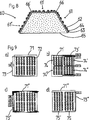
In
Mit Linien sind Lichtkegel
Ist die mit LED-Chips
In
Sowohl in
In
In
In den
So ist in
In
In
In
Prinzipiell können LEDs
In
In
In
Die Geometrie der Beleuchtungsvorrichtung
In
Eine Beleuchtungsvorrichtung
Weiterhin können in der Beleuchtungseinheit
In
Das Koordinatensystem in
Alle genannten Merkmale, auch die den Zeichnungen allein zu entnehmenden sowie auch einzelne Merkmale, die in Kombination mit anderen Merkmalen offenbart sind, werden allein und in Kombination als erfindungswesentlich angesehen. Erfindungsgemäße Ausführungsformen können durch einzelne Merkmale oder eine Kombination mehrerer Merkmale erfüllt sein.All mentioned features, including the drawings alone to be taken as well as individual features that are disclosed in combination with other features are considered alone and in combination as essential to the invention. Embodiments of the invention may be accomplished by individual features or a combination of several features.
BezugszeichenlisteLIST OF REFERENCE NUMBERS
- 11
- Chip-on-Board-LED-ModulChip-on-board LED module
- 2, 2'2, 2 '
- Substratsubstratum
- 3, 3'3, 3 '
- Leiterbahnconductor path
- 4, 4'4, 4 '
- LEDLED
- 5, 5'5, 5 '
- Lichtkegellight cone
- 66
- Stoßstellejoint
- 11, 11'11, 11 '
- Chip-on-Board-LED-ModulChip-on-board LED module
- 12, 12'12, 12 '
- Substratsubstratum
- 13, 13'13, 13 '
- Leiterbahnconductor path
- 14, 14'14, 14 '
- LEDLED
- 15, 15'15, 15 '
- Lichtkegellight cone
- 1616
- Stoßstellejoint
- 1717
- Bereich schwächerer AusleuchtungArea of weaker illumination
- 2121
- Chip-on-Board-LED-ModulChip-on-board LED module
- 2222
- Substratsubstratum
- 2323
- Leiterbahnconductor path
- 2424
- LEDLED
- 2525
- transparenter Deckeltransparent lid
- 28, 26'28, 26 '
- Randedge
- 2727
- Innenrauminner space
- 3131
- Chip-on-Board-LED-ModulChip-on-board LED module
- 3232
- Substratsubstratum
- 3333
- Leiterbahnconductor path
- 3434
- LEDLED
- 3535
- transparentes Vergussmaterialtransparent potting material
- 36, 36'36, 36 '
- Einhausunghousing
- 40, 40', 40''40, 40 ', 40' '
- Beleuchtungsvorrichtunglighting device
- 41, 41', 41''41, 41 ', 41' '
- Chip-on-Board-LED-ModulChip-on-board LED module
- 42, 42', 42''42, 42 ', 42' '
- Hohlkörperhollow body
- 45, 45', 45''45, 45 ', 45' '
- Beleuchtungsvorrichtunglighting device
- 46, 46', 46''46, 46 ', 46' '
- Chip-on-Board-LED-ModulChip-on-board LED module
- 47, 47', 47''47, 47 ', 47' '
- beleuchteter Körperilluminated body
- 50, 50', 50''50, 50 ', 50' '
- Beleuchtungsvorrichtunglighting device
- 51, 51', 51''51, 51 ', 51' '
- Chip-on-Board-LED-ModulChip-on-board LED module
- 52, 52', 52''52, 52 ', 52' '
- befeuchteter Körpermoistened body
- 5353
- plane Seite des Körpersplane side of the body
- 5454
- plane Seite der leuchtenden Oberflächeplane side of the glowing surface
- 5555
- Einbuchtung in der leuchtenden OberflächeDent in the luminous surface
- 5656
- Einbuchtung im KörperIndentation in the body
- 8080
- Beleuchtungsvorrichtunglighting device
- 61–61''61-61 ''
- Chip-on-Board-LED-ModulChip-on-board LED module
- 6262
- Substratsubstratum
- 6363
- Leiterbahnconductor path
- 6464
- LEDLED
- 6565
- Kühlkörperheatsink
- 66, 66'66, 66 '
- Stoßkanteimpact edge
- 71–71'''71-71 '' '
- Chip-on-Board-LED-ModulChip-on-board LED module
- 7272
- LEDLED
- 73–73'''73-73 '' '
- Schaltbild für StromkreisCircuit diagram for circuit
- 74–74'''74-74 '' '
- Quadrantquadrant
- 75, 75'75, 75 '
- Halbflächehalf area
- 8080
- Beleuchtungsvorrichtunglighting device
- 811–818 81 1 -81 8
- Chip-on-Board-LED-ModulChip-on-board LED module
- 8282
- Kühlkörperheatsink
- 8383
- Hohlraumcavity
- 8484
- Schutzglasprotective glass
- 8585
- Zwischenraumgap
- 9090
- mehrteilige Beleuchtungseinheitmulti-part lighting unit
- 9191
- Kontroll- und VersorgungseinheitControl and supply unit
- 9292
- Verbindungsleitungconnecting line
- 93–93'''93-93 '' '
- Beleuchtungsvorrichtunglighting device
- 94–94'''94-94 '' '
- Anschlusseinheitconnection unit
- 100100
- gemessene Leuchtkraftmeasured luminosity
- 101101
- mittlere Leuchtkraftmean luminosity
Claims (15)
Priority Applications (15)
| Application Number | Priority Date | Filing Date | Title |
|---|---|---|---|
| DE102010013286A DE102010013286B4 (en) | 2010-03-29 | 2010-03-29 | LED lamp for homogeneous illumination of hollow bodies |
| SI201130829A SI2553314T1 (en) | 2010-03-29 | 2011-03-25 | Led lamp for homogeneously illuminating hollow bodies |
| JP2013501676A JP5506999B2 (en) | 2010-03-29 | 2011-03-25 | LED lamp for uniformly illuminating the hollow body |
| ES11713180.5T ES2567180T3 (en) | 2010-03-29 | 2011-03-25 | LED lamp for homogeneous lighting of hollow bodies |
| PCT/EP2011/001510 WO2011124331A1 (en) | 2010-03-29 | 2011-03-25 | Led lamp for homogeneously illuminating hollow bodies |
| KR1020127025811A KR101389223B1 (en) | 2010-03-29 | 2011-03-25 | Led lamp for homogeneously illuminating hollow bodies |
| US13/637,661 US9188289B2 (en) | 2010-03-29 | 2011-03-25 | LED lamp for homogeneously illuminating hollow bodies |
| CN2011800168863A CN102812285A (en) | 2010-03-29 | 2011-03-25 | LED lamp for homogeneously illuminating hollow bodies |
| HUE11713180A HUE027957T2 (en) | 2010-03-29 | 2011-03-25 | Led lamp for homogeneously illuminating hollow bodies |
| PL11713180.5T PL2553314T3 (en) | 2010-03-29 | 2011-03-25 | Led lamp for homogeneously illuminating hollow bodies |
| CA2792814A CA2792814C (en) | 2010-03-29 | 2011-03-25 | Led lamp for homogeneously illuminating hollow bodies |
| EP11713180.5A EP2553314B1 (en) | 2010-03-29 | 2011-03-25 | Led lamp for homogeneously illuminating hollow bodies |
| BR112012024455A BR112012024455A2 (en) | 2010-03-29 | 2011-03-25 | led lamp for homogeneous hollow body lighting |
| CN201611014782.XA CN107101091A (en) | 2010-03-29 | 2011-03-25 | LED for equably irradiating hollow body |
| TW100110848A TWI499736B (en) | 2010-03-29 | 2011-03-29 | Led lamp for homogeneous illumination of hollow bodies |
Applications Claiming Priority (1)
| Application Number | Priority Date | Filing Date | Title |
|---|---|---|---|
| DE102010013286A DE102010013286B4 (en) | 2010-03-29 | 2010-03-29 | LED lamp for homogeneous illumination of hollow bodies |
Publications (2)
| Publication Number | Publication Date |
|---|---|
| DE102010013286A1 DE102010013286A1 (en) | 2011-09-29 |
| DE102010013286B4 true DE102010013286B4 (en) | 2012-03-22 |
Family
ID=44262814
Family Applications (1)
| Application Number | Title | Priority Date | Filing Date |
|---|---|---|---|
| DE102010013286A Active DE102010013286B4 (en) | 2010-03-29 | 2010-03-29 | LED lamp for homogeneous illumination of hollow bodies |
Country Status (14)
| Country | Link |
|---|---|
| US (1) | US9188289B2 (en) |
| EP (1) | EP2553314B1 (en) |
| JP (1) | JP5506999B2 (en) |
| KR (1) | KR101389223B1 (en) |
| CN (2) | CN107101091A (en) |
| BR (1) | BR112012024455A2 (en) |
| CA (1) | CA2792814C (en) |
| DE (1) | DE102010013286B4 (en) |
| ES (1) | ES2567180T3 (en) |
| HU (1) | HUE027957T2 (en) |
| PL (1) | PL2553314T3 (en) |
| SI (1) | SI2553314T1 (en) |
| TW (1) | TWI499736B (en) |
| WO (1) | WO2011124331A1 (en) |
Families Citing this family (45)
| Publication number | Priority date | Publication date | Assignee | Title |
|---|---|---|---|---|
| DE102011107895B4 (en) | 2011-07-18 | 2020-11-05 | Heraeus Noblelight Gmbh | Optoelectronic module with lens system |
| JP5762334B2 (en) * | 2012-02-20 | 2015-08-12 | シャープ株式会社 | Lighting device |
| JP6133017B2 (en) * | 2012-04-27 | 2017-05-24 | 京セラメディカル株式会社 | Membrane manufacturing apparatus and artificial joint component manufacturing method |
| DE102012008638A1 (en) * | 2012-05-02 | 2013-11-07 | Heraeus Noblelight Gmbh | Luminaire with LEDs and cylindrical lens |
| TWI505440B (en) * | 2012-06-04 | 2015-10-21 | Lextar Electronics Corp | Light source module |
| US8974077B2 (en) | 2012-07-30 | 2015-03-10 | Ultravision Technologies, Llc | Heat sink for LED light source |
| JP5591305B2 (en) * | 2012-10-30 | 2014-09-17 | 株式会社トクヤマ | Ultraviolet light emitting module and ultraviolet irradiation device |
| USD706960S1 (en) | 2013-02-19 | 2014-06-10 | NanoGrid Limited Hong Kong | LED bulb |
| CN104075142A (en) | 2013-03-26 | 2014-10-01 | 纳米格有限公司 | Led lamp |
| JP6075542B2 (en) * | 2013-02-20 | 2017-02-08 | 東芝ライテック株式会社 | Light emitting device and lighting device |
| US8974078B2 (en) * | 2013-04-03 | 2015-03-10 | Litatek Corporation | Lamp with enhanced lighting angle |
| TWI550231B (en) * | 2013-08-19 | 2016-09-21 | de-long Chen | Lamps and their flexible conductive devices |
| US9706609B2 (en) * | 2013-09-11 | 2017-07-11 | Heraeus Noblelight America Llc | Large area high-uniformity UV source with many small emitters |
| CN104576876B (en) * | 2013-10-28 | 2017-10-31 | 四川新力光源股份有限公司 | One-piece type circular cone COB encapsulated LED light sources and preparation method thereof |
| TW201525357A (en) * | 2013-12-23 | 2015-07-01 | Skynet Electronic Co Ltd | LED light bulb with a bi-directional axle convection type heat sink structure |
| US9195281B2 (en) | 2013-12-31 | 2015-11-24 | Ultravision Technologies, Llc | System and method for a modular multi-panel display |
| WO2015197042A2 (en) * | 2014-06-23 | 2015-12-30 | Kronhagel Mediatecture Gmbh | Device, method for advertising, method for retrofitting a device, construction set and arrangement |
| CN104154455B (en) * | 2014-07-17 | 2017-03-15 | 江苏银晶光电科技发展有限公司 | LED reaction lamps and the optical chlorinating reaction kettle using which |
| USD742559S1 (en) * | 2014-10-24 | 2015-11-03 | Henry Gze Hin Chow | LED bulb |
| US9467190B1 (en) * | 2015-04-23 | 2016-10-11 | Connor Sport Court International, Llc | Mobile electronic device covering |
| US10918747B2 (en) | 2015-07-30 | 2021-02-16 | Vital Vio, Inc. | Disinfecting lighting device |
| CA2993825C (en) | 2015-07-30 | 2020-08-25 | Vital Vio, Inc. | Single diode disinfection |
| DE102015117206A1 (en) * | 2015-10-08 | 2017-04-13 | I.S.T. Innovative Sewer Technologies Gmbh | Curing device with a UV light-generating lamp |
| WO2018019655A1 (en) * | 2016-07-26 | 2018-02-01 | Philips Lighting Holding B.V. | A light emitting device |
| EP3321554B1 (en) * | 2016-10-18 | 2020-04-01 | Bolonia Servicios e Ingenieros, S.L. | A device for curing inner lining of a pipeline |
| DK3345740T3 (en) * | 2017-01-09 | 2019-07-29 | Bolonia Servicios E Ingenieros S L | DEVICE FOR CURRENCY OF INTERNAL RESIN PIPE LINES |
| US11118716B2 (en) | 2017-03-03 | 2021-09-14 | Ina Acquisition Corp. | Curing device for curing a pipe liner |
| CN106647192A (en) * | 2017-03-10 | 2017-05-10 | 深圳市华星光电技术有限公司 | Exposure equipment |
| DE102017107977A1 (en) | 2017-04-12 | 2018-10-18 | Bernd-Jan Krasowski | Apparatus for rehabilitating a pipeline by means of a lining fiber hose |
| US10700252B2 (en) * | 2017-04-18 | 2020-06-30 | Bridgelux Chongqing Co., Ltd. | System and method of manufacture for LED packages |
| RU2656604C1 (en) * | 2017-07-26 | 2018-06-06 | Федеральное государственное бюджетное учреждение науки Физический институт им. П.Н. Лебедева Российской академии наук (ФГБУН ФИАН) | Lighting device |
| US11674628B2 (en) | 2017-08-18 | 2023-06-13 | Moray Group, Llc | Method, apparatus and system for lining conduits |
| US10835627B2 (en) * | 2017-12-01 | 2020-11-17 | Vital Vio, Inc. | Devices using flexible light emitting layer for creating disinfecting illuminated surface, and related method |
| US10309614B1 (en) | 2017-12-05 | 2019-06-04 | Vital Vivo, Inc. | Light directing element |
| US10413626B1 (en) | 2018-03-29 | 2019-09-17 | Vital Vio, Inc. | Multiple light emitter for inactivating microorganisms |
| RU189452U1 (en) * | 2018-10-17 | 2019-05-22 | Закрытое акционерное общество "БТМ" | LED lamp |
| EP3690299B1 (en) * | 2019-02-04 | 2022-11-16 | Picote Solutions Inc. | Device for curing coating substance |
| US11639897B2 (en) | 2019-03-29 | 2023-05-02 | Vyv, Inc. | Contamination load sensing device |
| US11541135B2 (en) | 2019-06-28 | 2023-01-03 | Vyv, Inc. | Multiple band visible light disinfection |
| US11369704B2 (en) | 2019-08-15 | 2022-06-28 | Vyv, Inc. | Devices configured to disinfect interiors |
| EP3795880A1 (en) * | 2019-09-17 | 2021-03-24 | Sewertronics Sp. z o.o. | A device for curing pipeline inner resin linings |
| US11878084B2 (en) | 2019-09-20 | 2024-01-23 | Vyv, Inc. | Disinfecting light emitting subcomponent |
| CN114999316A (en) * | 2021-03-01 | 2022-09-02 | 南京瀚宇彩欣科技有限责任公司 | Pixel structure and flexible display device |
| RU209306U1 (en) * | 2021-07-29 | 2022-03-15 | Марат Габдулгазизович Бикмуллин | water cooled lamp |
| US11906133B2 (en) | 2022-03-31 | 2024-02-20 | Alliance Sports Group, L.P. | Outdoor lighting apparatus |
Citations (4)
| Publication number | Priority date | Publication date | Assignee | Title |
|---|---|---|---|---|
| EP1357331A2 (en) * | 2002-04-25 | 2003-10-29 | Yuan Lin | Flexible rod light device formed of chip on board based LED lamps and manufacturing method thereof |
| US20050024870A1 (en) * | 2002-04-09 | 2005-02-03 | Coushaine Charles M. | LED light source assembly |
| US20090016072A1 (en) * | 2007-07-12 | 2009-01-15 | Foxconn Technology Co., Ltd. | Led lamp with a heat dissipation device |
| US20100051168A1 (en) * | 2007-02-19 | 2010-03-04 | Ole Moeskjaer | Apparatus and a method for curing a liner of a pipeline |
Family Cites Families (25)
| Publication number | Priority date | Publication date | Assignee | Title |
|---|---|---|---|---|
| ES2289822T3 (en) * | 1998-09-17 | 2008-02-01 | Koninklijke Philips Electronics N.V. | LED LAMP. |
| JP2002184207A (en) * | 2000-12-15 | 2002-06-28 | Matsushita Electric Ind Co Ltd | Led illumination bulb |
| JP3851174B2 (en) | 2001-01-25 | 2006-11-29 | 松下電器産業株式会社 | Light emitting unit, light emitting unit combination, and lighting device |
| JP2007059930A (en) | 2001-08-09 | 2007-03-08 | Matsushita Electric Ind Co Ltd | Led lighting fixture and card type led lighting light source |
| AU2002365761A1 (en) * | 2001-11-16 | 2003-06-17 | Toyoda Gosei Co., Ltd. | Light-emitting diode, led light, and light apparatus |
| US20030235800A1 (en) * | 2002-06-24 | 2003-12-25 | Qadar Steven Abdel | LED curing light |
| US20050169006A1 (en) * | 2004-01-30 | 2005-08-04 | Harvatek Corporation | Led chip lamp apparatus |
| US7070311B2 (en) * | 2004-06-03 | 2006-07-04 | Fu An Industrial Co., Ltd. | Vehicle light for producing light whose form depends on orientations of plural refraction elements |
| US7829899B2 (en) * | 2006-05-03 | 2010-11-09 | Cree, Inc. | Multi-element LED lamp package |
| CN101126485A (en) * | 2006-08-18 | 2008-02-20 | 蒋承庭 | Light source module possessing LED and its forming method |
| JP2008142996A (en) * | 2006-12-08 | 2008-06-26 | S G C Gesuido Center Kk | Method for lining piping and photocuring apparatus |
| JP2008175381A (en) | 2007-01-18 | 2008-07-31 | Bkp Berolina Polyester Gmbh & Co Kg | Curing renovation device having led |
| JP4964015B2 (en) * | 2007-04-24 | 2012-06-27 | 吉佳株式会社 | Photocuring method for photocurable lining material and photocuring system used for the method |
| JP2008277174A (en) | 2007-04-27 | 2008-11-13 | Litehouse Technologies Corp | Light emission device and its mounting frame |
| ES2748331T3 (en) | 2007-05-02 | 2020-03-16 | Signify Holding Bv | Solid state lighting device |
| DE102007038197A1 (en) | 2007-08-14 | 2009-02-19 | Brandenburger Patentverwertung GbR (vertretungsberechtigter Gesellschafter: Wilhelm Leo Betz, 76887 Bad Bergzabern) | Method and device for rehabilitating pipelines |
| DE102007038196A1 (en) | 2007-08-14 | 2009-02-19 | Brandenburger Patentverwertung GbR (vertretungsberechtigter Gesellschafter: Wilhelm Leo Betz, 76887 Bad Bergzabern) | Method of rehabilitating branch pipes in sewer pipes |
| KR20090006121U (en) | 2007-12-17 | 2009-06-22 | 추 야오 우 | Light emitting diode lamp |
| DE102008010167B4 (en) | 2008-02-20 | 2018-10-25 | Brandenburger Patentverwertung GbR (vertretungsberechtigter Gesellschafter: Tim Brandenburger, 76829 Landau) | Apparatus and method for curing resin impregnated fiber hoses |
| US20100001664A1 (en) * | 2008-02-26 | 2010-01-07 | Shu-Chuan Shih | Illuminating fabric product |
| JP2009277586A (en) * | 2008-05-16 | 2009-11-26 | San Corporation Kk | Electric lamp type led luminaire |
| DE112009001774B4 (en) * | 2008-07-24 | 2020-10-01 | Tridonic Gmbh & Co Kg | Light source with LED, emergency route lighting and method for evenly illuminating an area |
| EP2151617A1 (en) | 2008-08-05 | 2010-02-10 | Per Aarsleff A/S | Pipeline sealing apparatus, method of sealing a pipeline and a sealing system |
| JP2010055993A (en) * | 2008-08-29 | 2010-03-11 | Toshiba Lighting & Technology Corp | Lighting system and luminaire |
| US8342733B2 (en) * | 2009-12-14 | 2013-01-01 | Tyco Electronics Corporation | LED lighting assemblies |
-
2010
- 2010-03-29 DE DE102010013286A patent/DE102010013286B4/en active Active
-
2011
- 2011-03-25 EP EP11713180.5A patent/EP2553314B1/en active Active
- 2011-03-25 CA CA2792814A patent/CA2792814C/en active Active
- 2011-03-25 BR BR112012024455A patent/BR112012024455A2/en not_active Application Discontinuation
- 2011-03-25 KR KR1020127025811A patent/KR101389223B1/en active IP Right Grant
- 2011-03-25 HU HUE11713180A patent/HUE027957T2/en unknown
- 2011-03-25 ES ES11713180.5T patent/ES2567180T3/en active Active
- 2011-03-25 JP JP2013501676A patent/JP5506999B2/en active Active
- 2011-03-25 SI SI201130829A patent/SI2553314T1/en unknown
- 2011-03-25 PL PL11713180.5T patent/PL2553314T3/en unknown
- 2011-03-25 WO PCT/EP2011/001510 patent/WO2011124331A1/en active Application Filing
- 2011-03-25 CN CN201611014782.XA patent/CN107101091A/en active Pending
- 2011-03-25 CN CN2011800168863A patent/CN102812285A/en active Pending
- 2011-03-25 US US13/637,661 patent/US9188289B2/en active Active
- 2011-03-29 TW TW100110848A patent/TWI499736B/en not_active IP Right Cessation
Patent Citations (4)
| Publication number | Priority date | Publication date | Assignee | Title |
|---|---|---|---|---|
| US20050024870A1 (en) * | 2002-04-09 | 2005-02-03 | Coushaine Charles M. | LED light source assembly |
| EP1357331A2 (en) * | 2002-04-25 | 2003-10-29 | Yuan Lin | Flexible rod light device formed of chip on board based LED lamps and manufacturing method thereof |
| US20100051168A1 (en) * | 2007-02-19 | 2010-03-04 | Ole Moeskjaer | Apparatus and a method for curing a liner of a pipeline |
| US20090016072A1 (en) * | 2007-07-12 | 2009-01-15 | Foxconn Technology Co., Ltd. | Led lamp with a heat dissipation device |
Also Published As
| Publication number | Publication date |
|---|---|
| WO2011124331A1 (en) | 2011-10-13 |
| EP2553314B1 (en) | 2016-02-24 |
| JP5506999B2 (en) | 2014-05-28 |
| HUE027957T2 (en) | 2016-11-28 |
| KR101389223B1 (en) | 2014-04-24 |
| US9188289B2 (en) | 2015-11-17 |
| DE102010013286A1 (en) | 2011-09-29 |
| KR20120138795A (en) | 2012-12-26 |
| SI2553314T1 (en) | 2016-06-30 |
| BR112012024455A2 (en) | 2016-05-31 |
| CN107101091A (en) | 2017-08-29 |
| CN102812285A (en) | 2012-12-05 |
| TWI499736B (en) | 2015-09-11 |
| CA2792814A1 (en) | 2011-10-13 |
| CA2792814C (en) | 2015-02-17 |
| PL2553314T3 (en) | 2016-09-30 |
| US20130010460A1 (en) | 2013-01-10 |
| EP2553314A1 (en) | 2013-02-06 |
| ES2567180T3 (en) | 2016-04-20 |
| TW201202601A (en) | 2012-01-16 |
| JP2013524415A (en) | 2013-06-17 |
Similar Documents
| Publication | Publication Date | Title |
|---|---|---|
| DE102010013286B4 (en) | LED lamp for homogeneous illumination of hollow bodies | |
| DE102011107895B4 (en) | Optoelectronic module with lens system | |
| EP2614694B1 (en) | Coating method for an optoelectronic chip-on-board module | |
| EP2459924B1 (en) | Lighting device with led's | |
| EP1528388B1 (en) | UV light emission diodes as radiation source of a device for the artificial weathering of samples | |
| DE102012008638A1 (en) | Luminaire with LEDs and cylindrical lens | |
| EP2743564B2 (en) | Lighting device and illumination arrangement for lighting the interior of a tower or tunnel | |
| EP3190617B1 (en) | Light emitting device and method of fabricating a light emitting device | |
| DE212013000056U1 (en) | Edge weighted distance of LEDS for area of improved uniformity | |
| EP2326962B1 (en) | Device for testing solar cells | |
| DE102011107892A1 (en) | Method for coating e.g. chip-on-board UV-LED module utilized in solar cell, involves curing and cross-linking liquid silicone with optoelectronic components and carriers, and removing carrier with hardened silicone coating from mold | |
| DE102008031930B4 (en) | Lighting device with micro lens array | |
| DE102014205470A1 (en) | Lighting device with CoB range | |
| DE102016224341A1 (en) | Headlamp and headlamp module for a headlamp | |
| EP2748515B1 (en) | Light source device | |
| DE102014100141B4 (en) | Irradiation device for irradiation of plants | |
| DE4109895A1 (en) | Elongated electrodeless discharge lamp bulb contg. plasma source - has limits of discharge space speed. from walls to improve substrate irradiation by ends of reflector | |
| DE202015007511U1 (en) | Led lamp |
Legal Events
| Date | Code | Title | Description |
|---|---|---|---|
| R016 | Response to examination communication | ||
| R018 | Grant decision by examination section/examining division | ||
| R020 | Patent grant now final |
Effective date: 20120623 |
|
| R082 | Change of representative |
Representative=s name: BRAND, NORMEN, DR. RER. NAT., DE Representative=s name: BRAND, NORMEN, DIPL.-CHEM. UNIV. DR. RER. NAT., DE Representative=s name: EULER, MATTHIAS, DR., DE |
|
| R082 | Change of representative |
Representative=s name: BRAND, NORMEN, DR. RER. NAT., DE Representative=s name: BRAND, NORMEN, DIPL.-CHEM. UNIV. DR. RER. NAT., DE |
|
| R082 | Change of representative |
Representative=s name: MEWBURN ELLIS LLP, DE |