Hintergrund der ErfindungBackground of the invention
1. Gebiet der Erfindung1. Field of the invention
Die vorliegende Erfindung betrifft im Allgemeinen Messfühlerkarten und insbesondere einen Messfühler bzw. eine Sonde, die dazu geeignet ist, in einer Messfühlerkarte für eine Hochfrequenz-Signalübertragung verwendet zu werden.The present invention relates generally to probe cards and, more particularly, to a probe suitable for use in a probe card for high frequency signal transmission.
2. Beschreibung des Standes der Technik2. Description of the Related Art
1 zeigt eine Sonde bzw. einen Messfühler 1 von Kragarm-Typ gemäß der US 6,727,716 und US 6,603,322 . Entsprechend dieser Gestaltung umfasst die Sonde 1 vom Kragarm-Typ eine Platine 10, mehrere koaxiale Übertragungsleitungen 11, die um den äußeren Bereich der Platine 10 angeordnet vorliegen, einen Sondenhalter 12, der an dem inneren Bereich der Platine 10 angeordnet vorliegt und mehrere koaxiale Sonden 20. Der Sondenhalter 20 umfasst eine isolierte Basis 121, die aus einem einen Schock absorbierenden elektrisch isolierten Material hergestellt ist, einen Erdungs-Aufbau 122, der aus einem metallischen Material hergestellt und an der isolierten Basis 121 angeordnet und mit dem/der Erdungspotential bzw. -masse der Messfühlerkarte 1 des Kragarm-Typs elektrisch verbunden vorliegt und mehrere Lokalisierungs-Elemente 123, die an dem Erdungsaufbau 122 starr bereitgestellt sind, um die koaxialen Sonden 20 zu sichern. Die Sonden 20 umfassen jeweils einen Metallstift 21, der einen vorderen Teil 201 (der Teil zwischen dem entsprechenden Lokalisierungs-Element 123 und der Sondenspitze des entsprechenden Metallstifts 21) und einen hinteren Teil 202 (der Teil zwischen dem entsprechenden Lokalisierungs-Element 123 und der Platine 10) aufweist, eine dielektrische Schicht 22, die den hinteren Teil 202 umgibt, und eine metallische stromführende bzw. leitfähige Schicht 23, die die dielektrische Abdeckung 22 umgibt. Die metallische stromführende Schicht 23 steht mit dem Erdungsaufbau 122 in Kontakt, um so mit dem Erdungspotential elektrisch verbunden zu sein. Folglich wird, während der Weiterleitung eines Hochfrequenz-Signals, von der koaxialen Struktur des hinteren Endes von jeder koaxialen Sonde 20 eine charakteristische Impedanz wirksam beibehalten. 1 shows a probe or a probe 1 of cantilever type according to the US 6,727,716 and US 6,603,322 , According to this design, the probe includes 1 a cantilever-type board 10 , several coaxial transmission lines 11 around the outer area of the board 10 arranged, a probe holder 12 which is attached to the inner area of the board 10 arranged and several coaxial probes 20 , The probe holder 20 includes an isolated base 121 made of a shock absorbing electrically insulated material, a grounding structure 122 made of a metallic material and attached to the insulated base 121 arranged and with the / the earth potential or mass of the probe card 1 of the cantilever type is electrically connected and multiple localization elements 123 attached to the grounding structure 122 are rigidly provided to the coaxial probes 20 to secure. The probes 20 each include a metal pin 21 , the one front part 201 (the part between the corresponding localization element 123 and the probe tip of the corresponding metal pin 21 ) and a back part 202 (the part between the corresponding localization element 123 and the board 10 ), a dielectric layer 22 that the rear part 202 surrounds, and a metallic current-carrying or conductive layer 23 containing the dielectric cover 22 surrounds. The metallic current-carrying layer 23 stands with the grounding structure 122 in contact so as to be electrically connected to the grounding potential. Consequently, while transmitting a high-frequency signal, the coaxial structure of the rear end of each coaxial probe 20 effectively maintain a characteristic impedance.
Da der vordere Teil 201 von jeder koaxialen Sonde 20 so gestaltet vorliegt, um als ein elastischer Hebelarm zum Tragen und Puffer der Reaktionskraft zu dienen, die von der Sondenspitze zurückgeführt wird, dann ist, um deren Bewegungen ausführen zu können, ein ausreichender Umgebungsraum erforderlich, falls die Sondenspitze die Test- bzw. Prüfstelle auf einem zu untersuchenden Wafer testet bzw. abtastet. Folglich kann der vordere Teil 201 nicht so gestaltet sein, dass er eine koaxiale Struktur wie der hintere Teil 202 aufweist, d. h. die Aufrechterhaltung einer charakteristischen Impedanz während einer Hochfrequenz-Weiterleitung ist auf die hinteren Teile 202 der koaxialen Sonden 20 beschränkt, die an den vorderen Teilen 201 der koaxialen Sonden 20 nicht verfügbar sind. Folglich kann der durch die umgebende dielektrische Umgebung um jede koaxiale Sonde 20 induzierte parasitische Kondensator während einer Hochfrequenz-Signalübertragung einen dielektrischen Verlust bewirken.Because the front part 201 from each coaxial probe 20 is designed to serve as an elastic lever arm for carrying and buffering the reaction force returned from the probe tip, sufficient space is required to perform its movements if the probe tip is on the test site a wafer to be examined tests or scans. Consequently, the front part 201 not be designed so that it has a coaxial structure like the back part 202 ie, the maintenance of a characteristic impedance during a high-frequency transmission is on the rear parts 202 the coaxial probes 20 limited to the front parts 201 the coaxial probes 20 are not available. As a result, the surrounding dielectric environment can surround each coaxial probe 20 induced parasitic capacitor cause a dielectric loss during high-frequency signal transmission.
Da weiterhin der metallische Stift 21 einer jeden koaxialen Sonde 20 durch eine bestimmte Dicke bzw. Stärke einer dielektrischen Schicht umgeben sein muss, um die erwünschte charakteristische Impedanz der Signalübertragung beizubehalten, und bei der Installation der dielektrischen Schicht 22 muss der dielektrische Verlust berücksichtigt werden, der durch den parasitischen Kondensator zwischen dem metallischen Stift 21 und der stromführenden metallischen Schicht 23 bewirkt wird, so dass, um die Erzeugung einer fehlangepassten Impedanz zu vermeiden, das umgebende isolierte Material eine optimale Dicke aufweisen muss, die mit der Dielektrizitätskonstante variiert. Welches isolierte bzw. isolierende Material auch gewählt wird, der Durchmesser der koaxialen Sonde 20 ist weitaus größer als der Durchmesser des metallischen Stifts 21, wodurch die Anordnungsdichte der Sonden 20 beschränkt wird. Folglich gestattet die im Stand der Technik vorstehend erwähnte Messfühlerkarte von Kragarm-Typ nicht, dass elektronische Einrichtungen mit einer großen Anzahl von Sonden mit einem Hochfrequenzsignalisieren getestet werden. Die US 5,382,898 betrifft einen Messfühler für eine Hochfrequenz-Signalübertragung. Der Fühler umfasst unter anderem einen von einer Isolationsschicht umgebenen metallischen Stift und eine metallische Leitung.Because the metallic pin continues 21 each coaxial probe 20 must be surrounded by a certain thickness of a dielectric layer in order to maintain the desired characteristic impedance of the signal transmission, and in the installation of the dielectric layer 22 Consider the dielectric loss caused by the parasitic capacitor between the metallic pin 21 and the current-carrying metallic layer 23 so that in order to avoid generation of a mismatched impedance, the surrounding isolated material must have an optimum thickness that varies with the dielectric constant. Whichever insulated material is chosen, the diameter of the coaxial probe 20 is much larger than the diameter of the metallic pin 21 , whereby the arrangement density of the probes 20 is limited. Consequently, the cantilever type probe card mentioned in the prior art does not allow electronic devices with a large number of probes to be tested with high frequency signaling. The US 5,382,898 relates to a sensor for a high-frequency signal transmission. The sensor includes, inter alia, a metallic pin surrounded by an insulating layer and a metallic lead.
Zusammenfassung der ErfindungSummary of the invention
Die durch die vorliegende Erfindung bereitgestellte Sonde für eine Hochfrequenz-Signalübertragung umfasst einen metallischen Stift, der eine Sondenspitze aufweist, einen hinteren Bereich und einen Positionierungsbereich zwischen der Sondenspitze und dem hinteren Bereich, um eine Platine anzubringen;
mindestens eine metallische Leitung, die an dem metallischen Stift beabstandet angeordnet ist und zwei abgewandte Enden aufweist, die mit dem Erdungspotential elektrisch verbunden sind, und
mindestens eine isolierte Schicht, die zwischen dem metallischen Stift und der mindestens einen metallischen Leitung angeordnet vorliegt, worin die mindestens eine isolierte Schicht die mindestens eine metallische Leitung koaxial umgibt und eine bestimmte Wandstärke aufweist, die dem Abstand zwischen dem metallischen Stift und der mindestens einen metallischen Leitung entspricht.The high-frequency signal transmission probe provided by the present invention comprises a metallic pin having a probe tip, a rear portion, and a positioning portion between the probe tip and the rear portion to mount a circuit board;
at least one metallic lead spaced from the metallic pin and having two opposite ends electrically connected to the ground potential, and
at least one isolated layer between the metallic pin and the at least one metallic line is arranged, wherein the at least one insulated layer coaxially surrounds the at least one metallic line and has a certain wall thickness corresponding to the distance between the metallic pin and the at least one metallic line.
In einer hier nachfolgend ausführlich zu beschreibenden beispielhaften Ausführungsform umfasst die Sonde einen Leitungsdraht, der an dem vorstehend erwähnten metallischen Stift angebracht vorliegt. Der Leitungsdraht umfasst die vorstehend erwähnte metallische Leitung und die isolierte Schicht, die die metallische Leitung koaxial so umgibt, dass die metallische Leitung von dem metallischen Stift getrennt und elektrisch isoliert vorliegt.In an exemplary embodiment to be described in detail hereinafter, the probe includes a lead wire attached to the aforementioned metallic pin. The lead wire comprises the above-mentioned metallic lead and the insulated sheet coaxially surrounding the metallic lead so that the metallic lead is separated from the metallic lead and electrically isolated.
In einer anderen beispielhaften Ausführungsform liegt der metallische Stift durch die isolierte Schicht koaxial umgeben vor, so dass die metallische Leitung von dem metallischen Stift getrennt und isoliert vorliegt.In another exemplary embodiment, the metallic pin is coaxially surrounded by the insulated layer so that the metallic lead is isolated from the metallic pin and isolated.
In noch einer anderen beispielhaften Ausführungsform umfasst die Sonde zwei oder mehrere Leitungsdrähte, die an dem metallischen Stift angebracht vorliegen.In yet another exemplary embodiment, the probe includes two or more lead wires attached to the metallic pin.
Die durch die vorliegende Erfindung bereitgestellte Messfühlerkarte umfasst eine Platine, einen Sondenhalter, mehrere Signalsonden und mehrere Erdungssonden. Die Platine definiert eine obere Oberfläche und eine untere Oberfläche. Die obere Oberfläche wird mit einer Testmaschine zum Testen bzw. Prüfen von elektronischen Einrichtungen elektrisch verbunden. Die Platine weist darauf angeordnet mehrere Signalschaltungen und Erdungsschaltungen auf. Die Signalschaltungen und die Erdungsschaltungen sind so angeordnet, dass mindestens eine Erdungsschaltung angrenzend bzw. benachbart zu einer Signalschaltung beabstandet angeordnet vorliegt. Die Erdungsschaltungen sind mit dem/der Erdungspotential bzw. -masse elektrisch verbunden. Der Sondenhalter ist an der unteren Oberfläche der Platine angebracht. Die Signalsonden umfassen jeweils einen metallischen Stift und mindestens einen Leitungsdraht, der an dem metallischen Stift angeordnet und davon elektrisch isoliert und mit den Erdungssonden elektrisch verbunden vorliegt. Die metallischen Stifte der Signalsonden und der Erdungssonden weisen jeweils eine Sondenspitze auf, einen hinteren Bereich, und einen Positionierungsbereich, der zwischen dem hinteren Bereich und der Sondenspitze lokalisiert vorliegt. Der Positionierungsbereich wird an dem Sondenhalter gesichert. Die hinteren Bereiche der metallischen Stifte der Signalsonden sind mit den Signalschaltungen elektrisch verbunden. Die hinteren Bereiche der Erdungssonden sind mit den Erdungsschaltungen elektrisch verbunden.The probe card provided by the present invention includes a circuit board, a probe holder, multiple signal probes, and multiple ground probes. The board defines an upper surface and a lower surface. The upper surface is electrically connected to a test machine for testing electronic devices. The board has arranged thereon a plurality of signal circuits and ground circuits. The signal circuits and the grounding circuits are arranged such that at least one grounding circuit is disposed adjacent to a signal circuit and spaced apart. The ground circuits are electrically connected to the ground potential (ground). The probe holder is attached to the lower surface of the board. The signal probes each include a metallic pin and at least one lead wire disposed on and electrically insulated from the metallic pin and electrically connected to the ground probes. The metallic pins of the signal probes and the ground probes each have a probe tip, a rear region, and a positioning region located between the posterior region and the probe tip. The positioning area is secured to the probe holder. The rear portions of the metallic pins of the signal probes are electrically connected to the signal circuits. The rear portions of the ground probes are electrically connected to the ground circuits.
Gemäß einer anderen Ausführungsform der vorliegenden Erfindung weist die Messfühlerkarte unterschiedliche Signalwege zum Übertragen eines Testsignals und des entsprechenden resultierenden Abtastsignals auf, um eine Interferenz zwischen dem Testsignal und dem Abtastsignal zu verhindern. Gemäß dieser Ausführungsform umfasst die Messfühlerkarte eine Platine, einen Sondenhalter, mehrere Signalsonden, und mehrere Erdungssonden. Die Platine definiert eine obere Oberfläche und eine von der oberen Oberfläche abgewandte untere Oberfläche. Die obere Oberfläche wird mit einer Testmaschine zum Testen bzw. Prüfen elektronischer Einrichtungen elektrisch verbunden. Die Platine weist darauf angeordnet mehrere Signalschaltungen und Erdungsschaltungen auf. Die Signalschaltungen und die Erdungsschaltungen sind so angeordnet, dass mindestens eine Erdungsschaltung benachbart zu einer Signalschaltung angeordnet vorliegt und mit einem bestimmten Abstand von der Signalschaltung getrennt gehalten wird. Die Erdungsschaltungen sind mit dem Erdungspotential elektrisch verbunden. Die Signalschaltungen umfassen jeweils einen Treiber- bzw. Messsignalführungs- bzw. Treiberdraht (forcing wire) und einen Abtastdraht. Der Treiberdraht ist dazu geeignet ein Testsignal von einer Testmaschine zu einer Testprobe weiterzuleiten. Der Abtastdraht ist dazu geeignet, ein Testsignal von dem entsprechenden Testergebnis von der Testprobe zu der Testmaschine zu übertragen. Der Sondenhalter ist an der unteren Oberfläche der Platine angebracht. Die Signalsonden umfassen jeweils einen metallischen Stift und mindestens einen Leitungsdraht, der an dem metallischen Stift angeordnet vorliegt und zwei distale Enden aufweist, die jeweils mit dem metallischen Stift und dem Abtastdraht von einem der Signalschaltungen elektrisch verbunden sind. Die Erdungssonden sind dazu geeignet, dass mindestens eine Erdungssonde benachbart zu jeder der Signalsonden angeordnet und von der benachbarten Signalsonde mit einem bestimmten Abstand beabstandet ist. Die metallischen Stifte der Signalsonden und Erdungssonden weisen jeweils eine Sondenspitze auf, einen hinteren Bereich und einen Positionierungsbereich, der zwischen dem hinteren Bereich und der Sondenspitze lokalisiert vorliegt. Der Positionierungsbereich wird an dem Sondenhalter gesichert. Die hinteren Bereiche der metallischen Stifte der Signalsonden sind mit den Treiberdrähten der Signalschaltungen elektrisch verbunden. Die hinteren Bereiche der Erdungssonden sind mit den Erdungsschaltungen elektrisch verbunden.According to another embodiment of the present invention, the probe card has different signal paths for transmitting a test signal and the corresponding resulting strobe signal to prevent interference between the test signal and the strobe signal. According to this embodiment, the probe card comprises a board, a probe holder, a plurality of signal probes, and a plurality of ground probes. The board defines an upper surface and a lower surface remote from the upper surface. The upper surface is electrically connected to a test machine for testing electronic devices. The board has arranged thereon a plurality of signal circuits and ground circuits. The signal circuits and the grounding circuits are arranged such that at least one grounding circuit is disposed adjacent to a signal circuit and kept separated from the signal circuit by a certain distance. The grounding circuits are electrically connected to the ground potential. The signal circuits each include a forcing wire and a sense wire. The driver wire is adapted to pass a test signal from a test machine to a test sample. The sensing wire is adapted to transmit a test signal from the corresponding test result from the test sample to the testing machine. The probe holder is attached to the lower surface of the board. The signal probes each include a metallic pin and at least one lead wire disposed on the metallic pin and having two distal ends respectively electrically connected to the metallic pin and the sensing wire of one of the signal circuits. The ground probes are adapted to have at least one ground probe disposed adjacent to each of the signal probes and spaced from the adjacent signal probe by a predetermined distance. The metallic pins of the signal probes and ground probes each have a probe tip, a posterior region, and a locating region located between the posterior region and the probe tip. The positioning area is secured to the probe holder. The rear portions of the metallic pins of the signal probes are electrically connected to the driver wires of the signal circuits. The rear portions of the ground probes are electrically connected to the ground circuits.
Ausführliche Beschreibung der ZeichnungenDetailed description of the drawings
Die vorliegende Erfindung wird aus der hier nachfolgend gegebenen und den begleitenden Zeichnungen, die lediglich für Erläuterungszwecke gegebenen sind, noch vollständiger verstanden werden und sind folglich für die vorliegende Erfindung nicht beschränkend, und worin:The present invention will become more fully understood from the accompanying drawings given hereinbelow, which are given by way of illustration only, and thus are not limitative of the present invention, and wherein:
1 eine schematische Schnittansicht einer Messfühlerkarte von Kragarm-Typ gemäß einer Gestaltung des Standes der Technik ist; 1 Fig. 12 is a schematic sectional view of a cantilever type probe card according to a prior art design;
2 eine Aufsicht auf eine Messfühlerkarte von Kragarm-Typ gemäß einer ersten erfindungsgemäßen Ausführungsform darstellt; 2 Fig. 10 is a plan view of a cantilever type probe card according to a first embodiment of the present invention;
3 eine schematische Schnittansicht in einem vergrößerten Maßstab eines Teils der Messfühlerkarte von Kragarm-Typ gemäß der ersten Ausführungsform der vorliegenden Erfindung darstellt; 3 Fig. 10 is a schematic sectional view on an enlarged scale of a part of the cantilever type probe card according to the first embodiment of the present invention;
4 eine untere Ansicht in einem vergrößerten Maßstab eines Teils der ersten erfindungsgemäßen Ausführungsform darstellt, die die Beziehung zwischen der Signalsonde und der Erdungssonde zeigt; 4 Fig. 10 is a bottom view on an enlarged scale of a part of the first embodiment of the present invention showing the relationship between the signal probe and the ground probe;
5 eine Schnittansicht entlang der Linie 5-5 von 3 darstellt, 5 a sectional view taken along the line 5-5 of 3 represents,
6 eine Schnittansicht entlang der Linie 6-6 von 3 darstellt; 6 a sectional view taken along the line 6-6 of 3 represents;
7 eine graphische Darstellung darstellt, die das Signal zeigt, das charakteristisch für die Signalsonde gemäß der ersten Ausführungsform der vorliegenden Erfindung ist; 7 Fig. 12 is a graph showing the signal characteristic of the signal probe according to the first embodiment of the present invention;
8 eine graphische Darstellung darstellt, die das Signal zeigt, das für eine Signalsonde charakteristisch ist, die ein relativ größeres Ausmaß als die Signalsonde aufweist, die für das in 7 gezeigt Signal charakteristisch ist; 8th FIG. 4 is a graph showing the signal characteristic of a signal probe that is relatively larger in magnitude than the signal probe used for the signal in FIG 7 shown signal is characteristic;
9 eine schematische Querschnittsansicht eines Signalstifts gemäß einer zweiten erfindungsgemäßen Ausführungsform ist; 9 a schematic cross-sectional view of a signal pin according to a second embodiment of the invention is;
10 eine schematische Querschnittsansicht eines Signalstifts gemäß einer dritten Ausführungsform der vorliegenden Erfindung darstellt; 10 Fig. 10 is a schematic cross-sectional view of a signal pin according to a third embodiment of the present invention;
11 eine schematische Schnittansicht einer Messfühlerkarte vom Kragarm-Typ gemäß einer vierten Ausführungsform der vorliegenden Erfindung darstellt; 11 Fig. 10 is a schematic sectional view of a cantilever-type probe card according to a fourth embodiment of the present invention;
12 eine vergrößerte untere Ansicht eines Teils der Messfühlerkarte vom Kragarm-Typ der in 11 gezeigten vierten Ausführungsform darstellt, die die Beziehung zwischen einer Signalsonde und den assoziierten Erdungssonden zeigt; 12 an enlarged bottom view of part of the cantilever-type probe card of FIG 11 4 shows the relationship between a signal probe and the associated ground probes;
13 eine schematische Schnittansicht einer Messfühlerkarte vom Kragarm-Typ gemäß einer fünften Ausführungsform der vorliegenden Erfindung darstellt; 13 Fig. 10 is a schematic sectional view of a cantilever type probe card according to a fifth embodiment of the present invention;
14 eine schematische Schnittansicht einer Messfühlerkarte vom Kragarm-Typ gemäß einer sechsten Ausführungsform der vorliegenden Erfindung darstellt; 14 Fig. 12 is a schematic sectional view of a cantilever type probe card according to a sixth embodiment of the present invention;
15 eine Querschnittsansicht einer Signalsonde für eine Messfühlerkarte vom Kragarm-Typ gemäß der sechsten Ausführungsform der vorliegenden Erfindung darstellt; 15 Fig. 10 is a cross-sectional view of a signal probe for a cantilever-type probe card according to the sixth embodiment of the present invention;
16 eine Querschnittsansicht einer Signalsonde für eine Messfühlerkarte vom Kragarm-Typ gemäß einer siebten Ausführungsform der vorliegenden Erfindung darstellt; und 16 Fig. 10 is a cross-sectional view of a signal probe for a cantilever-type probe card according to a seventh embodiment of the present invention; and
17 eine schematische Schnittansicht einer Messfühlerkarte vom Kragarm-Typ gemäß einer achten Ausführungsform der vorliegenden Erfindung darstellt. 17 FIG. 12 is a schematic sectional view of a cantilever-type probe card according to an eighth embodiment of the present invention. FIG.
Ausführliche Beschreibung der ErfindungDetailed description of the invention
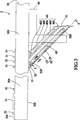
In den 2–5 umfasst eine Messfühlerkarte von Kragarm-Typ 2 zum Testen von Halbleiter-Wafern oder dergleichen gemäß einer ersten Ausführungsform der vorliegenden Erfindung eine Platine 30, einen Sondenhalter 40, mehrere Signalsonden 50 und mehrere Erdungssonden 60.In the 2 - 5 includes a probe card of cantilever type 2 For testing semiconductor wafers or the like according to a first embodiment of the present invention, a board 30 , a probe holder 40 , several signal probes 50 and several ground probes 60 ,
Wie in 2 und 3 gezeigt, definiert die Platine 30 eine obere Oberfläche 301 und eine der oberen Oberfläche 301 abgewandte untere Oberfläche 302 und ist in eine innere Untersuchungs- bzw. Abtastzone 303 und eine äußere Testzone 304 um die innere Untersuchungszone 303 aufgeteilt. Die äußere Testzone 304 an der oberen Oberfläche 301 soll mit einer Testmaschine (nicht gezeigt) elektrisch verbunden werden, die so gesteuert werden kann, dass sie an eine Messfühlerkarte 2 ein elektrisches Testsignal ausgibt, um der inneren Untersuchungszone 303 ein Hochfrequenz-Testsignal bereitzustellen. Die Platine 30 weist darauf angeordnet elektronische Schaltungen auf, einschließlich Signalschaltungen 31 und Erdungsschaltungen 32, die sich von der oberen Oberfläche 301 zu der unteren Oberfläche 302 erstrecken und mit den Signalsonden 50 und den Erdungssonden 60 elektrisch verbunden sind. Die Signalschaltungen 31 sind geeignet das vorstehend erwähnte Hochfrequenz-Testsignal weiterzuleiten. Die Erdungsschaltungen 32 sind jeweils mit einem bestimmten Abstand von den Signalschaltungen 31 beabstandet. Die Erdungsschaltungen 32 sind unmittelbar oder indirekt mit dem Erdungspotential der Testmaschine verbunden, um auf Übertragung des vorstehend erwähnten Hochfrequenz-Testsignals die charakteristische Impedanz der Signalschaltungen 31 aufrechtzuerhalten.As in 2 and 3 shown, defines the board 30 an upper surface 301 and one of the upper surface 301 remote lower surface 302 and is in an inner scanning zone 303 and an outer test zone 304 around the inner investigation zone 303 divided up. The outer test zone 304 on the upper surface 301 should be electrically connected to a test machine (not shown) that can be controlled to connect to a probe card 2 outputs an electrical test signal to the inner examination zone 303 to provide a high frequency test signal. The board 30 has arranged thereon electronic circuits, including signal circuits 31 and earthing circuits 32 extending from the upper surface 301 to the lower surface 302 extend and with the signal probes 50 and the ground probes 60 are electrically connected. The signal circuits 31 are suitable for passing the above-mentioned high-frequency test signal. The earthing circuits 32 are each at a certain distance from the signal circuits 31 spaced. The earthing circuits 32 are directly or indirectly connected to the grounding potential of the test machine in order to transmit the characteristic impedance of the signal circuits upon transmission of the aforementioned high-frequency test signal 31 maintain.
Der Sondenhalter 40 ist aus einem isolierten bzw. isolierenden Material, beispielsweise einem Epoxidharz, hergestellt und an der unteren Oberfläche 302 der Platine 30 in der inneren Untersuchungszone 303 ringförmig angebracht, um die Signalsonden 50 und die Erdungssonden 60 an Ort und Stelle zu halten und die Sonden 50 und 60 von einander isoliert zu halten.The probe holder 40 is made of an insulated material, such as a Epoxy resin, made and on the lower surface 302 the board 30 in the inner study zone 303 annularly attached to the signal probes 50 and the ground probes 60 to hold in place and the probes 50 and 60 to keep isolated from each other.
Erneut in den 3–5 umfasst jede Signalsonde 50 einen metallischen Stift 51 und einen Leitungsdraht 52. Der metallische Stift 51 ist an einem Ende in eine Untersuchungszone 511, einen hinteren Bereich 512 und einen Verbindungsbereich 513, einen Positionierungsbereich 514 und einen Hebelarm 515 aufgeteilt, der von einem hinteren Bereich in Richtung der Sondenspitze 511 integral angeordnet ist. Die Sondenspitze 511 ist geeignet das Testpad bzw. die Prüffläche 71 zu untersuchen, das/die an der elektronischen Einrichtung des untersuchten Halbleiter-Wafers bereitgestellt wird und so gestaltet ist, um ein Hochfrequenz-Testsignal zu empfangen. Der hintere Bereich 512 ist mit einer der Signalschaltungen 31 elektrisch verbunden. Der Positionierungsbereich 514 ist an dem Sondenhalter 40 befestigt. Der Leitungsdraht 52, der an dem Verbindungsbereich 513, dem Positionierungsbereich 514 und dem Hebelarm 515 des metallischen Stifts 51 angeordnet ist, umfasst eine metallische Leitung 520 und eine isolierte Schicht 521, die die metallische Leitung 520 koaxial umgibt. Die isolierte Schicht 521 von jedem Leitungsdraht 52 weist eine bestimmte Wanddicke bzw. -stärke auf, die die metallische Leitung 520 von dem metallischen Stift 51 isoliert. Die Erdungssonden 60 sind jeweils benachbart und parallel zu den Signalsonden 50 angeordnet. Die Erdungssonden 60 weisen die gleiche Struktur mit dem metallischen Stift 51 von jeder Signalsonde 50 auf. Jede Erdungssonde 60 ist an einem Ende in eine Sondenspitze 601, einen hinteren Bereich 602 und einen Verbindungsbereich 603, einen Positionierungsbereich 604 und einen Hebelarm 605 aufgeteilt, der von dem hinteren Bereich in Richtung der Sondenspitze 601 integral angeordnet ist. Die Sondenspitze 601 ist geeignet, um das Erdungspad bzw. die Masse- bzw. Erdungsfläche 72 zu untersuchen, das dem Erdungspotential der zu untersuchenden elektronischen Einrichtung entspricht. Der Positionierungsbereich 604 wird an dem Sondenhalter 40 befestigt. Die zwei Enden, die zu der Sondenspitze 601 und dem hinteren Bereich 602 benachbart vorliegen, sind jeweils mit der metallischen Leitung 520 des Leitungsdrahts 52 der benachbarten Signalsonde 50 verbunden.Again in the 3 - 5 includes each signal probe 50 a metallic pin 51 and a lead wire 52 , The metallic pen 51 is at one end in a study zone 511 , a rear area 512 and a connection area 513 , a positioning area 514 and a lever arm 515 split, from a rear area towards the tip of the probe 511 is arranged integrally. The probe tip 511 is suitable the test pad or the test area 71 which is provided at the electronic device of the semiconductor wafer under test and which is designed to receive a high-frequency test signal. The back area 512 is with one of the signal circuits 31 electrically connected. The positioning area 514 is on the probe holder 40 attached. The conductor wire 52 that is at the connection area 513 , the positioning area 514 and the lever arm 515 of the metallic pin 51 is arranged, comprises a metallic line 520 and an isolated layer 521 that the metallic wire 520 Coaxially surrounds. The isolated layer 521 from each wire 52 has a certain wall thickness or thickness, which is the metallic line 520 from the metallic pen 51 isolated. The earthing probes 60 are each adjacent and parallel to the signal probes 50 arranged. The earthing probes 60 have the same structure with the metallic pin 51 from each signal probe 50 on. Every earthing probe 60 is at one end into a probe tip 601 , a rear area 602 and a connection area 603 , a positioning area 604 and a lever arm 605 split that from the rear area towards the probe tip 601 is arranged integrally. The probe tip 601 is suitable for the grounding pad or the grounding surface 72 to investigate, which corresponds to the grounding potential of the electronic device to be examined. The positioning area 604 is attached to the probe holder 40 attached. The two ends leading to the probe tip 601 and the rear area 602 are adjacent, are each with the metallic line 520 of the conductor wire 52 the adjacent signal probe 50 connected.
Wie vorstehend erwähnt, werden von der Messfühlerkarte 2 vom Kragarm-Typ der vorliegenden Erfindung Signalsonden 50 verwendet, die jeweils aus einem metallischen Stift 51 und einem Leitungsdraht 52 gebildet sind, um die Gestaltung des Standes der Technik zu ersetzen, so dass jeder Übertragungsweg eines Hochfrequenz-Testsignals ein nahe gelegenes Erdungspotential aufweist und die zwei Enden der metallischen Leitung 520 des Leitungsdrahts 52, die sich benachbart zu der Sondenspitze 511 und dem hinteren Bereich 512 befinden, sind jeweils zu der benachbarten Erdungssonde 60 verbunden, um den charakteristischen Impedanzabgleich aufrechtzuerhalten, was eine Übertragungsqualität eines Hochfrequenz-Testsignals bereitstellt. Da weiterhin der metallische Stift 51 und der Leitungsdraht 52 von jeder Signalsonde 50 in paralleler Weise aneinander anliegen, wird der Durchmesser von jeder Signalsonde 50 abhängig von dem kombinierten Durchmesser des metallischen Stifts 51 und des Leitungsdrahts 52 bestimmt, wobei der maximale Durchmesser von jeder Signalsonde 50 ungefähr zweimal den Durchmesser des metallischen Stifts 52 oder kleiner, wie in 6 gezeigt, beträgt, und folglich besteht nicht die Notwendigkeit eine dielektrische Schicht bereitzustellen, die, wie die Sondenstruktur der Gestaltung des Standes der Technik, den metallischen Stift 51 einkapselt und eine stromführende metallische Schicht, die die dielektrische Abdeckung einkapselt. Die klein bemessene Sondengestaltung der vorliegenden Erfindung gestattet Signalsonden 50 in hoch dichter Weise in die innere Untersuchungszone 303 für einen Hochfrequenz-Test einzubauen, während immer noch ausreichend Pufferwirkung durch den Hebelarm 605 bereitgestellt wird, wenn die Sondenspitze die elektronische Einrichtung untersucht und einen charakteristischen Impedanzabgleich erreicht.As mentioned above, are from the probe card 2 cantilever type of the present invention signal probes 50 used, each consisting of a metallic pin 51 and a conductor wire 52 are formed to replace the prior art design such that each transmission path of a high frequency test signal has a nearby ground potential and the two ends of the metallic line 520 of the conductor wire 52 which is adjacent to the probe tip 511 and the rear area 512 are each to the adjacent grounding probe 60 connected to maintain the characteristic impedance balance, which provides a transmission quality of a high-frequency test signal. Because the metallic pin continues 51 and the conductor wire 52 from each signal probe 50 abutting each other in a parallel manner, the diameter of each signal probe 50 depending on the combined diameter of the metallic pin 51 and the conductor wire 52 determined, with the maximum diameter of each signal probe 50 about twice the diameter of the metallic pin 52 or smaller, as in 6 is shown, and thus there is no need to provide a dielectric layer which, like the probe structure of the prior art design, the metallic pin 51 encapsulates and a current-carrying metallic layer which encapsulates the dielectric cover. The small sized probe design of the present invention allows signal probes 50 in a high density into the inner investigation zone 303 for a high frequency test while still providing sufficient buffering by the lever arm 605 is provided when the probe tip examines the electronic device and achieves a characteristic impedance balance.
7 und 8 stellen charakteristische Frequenzkurven dar, die von erfindungsgemäß konstruierten Signalsonden erhalten wurden. Die in 7 gezeigte charakteristische Frequenzkurve wird von einer Signalsonde mit einem Abstand erhalten, der zwischen der Front-End-Kante der metallischen Leitung 520 und der Sondenspitze 511 des metallischen Stifts 51 160 Mil. beträgt und wobei der maximale kombinierte Durchmesser der Sonde 10 Mil. beträgt, in der der metallische Stift 51 und die metallische Leitung 520 den gleichen Durchmesser von 4 Mil. aufweisen und wobei die Wandstärke der isolierten Schicht 521 1 Mil. beträgt. Wie in 7 dargestellt, zeigt die Reflektions- bzw. Rückflussdämpfungs-Kurve S11 die geringe Rückflussdämpfung, während die Signalsonde für einen Hochfrequenzbetrieb bis zu einigen Giga-Hertz angewendet wird, wobei die Einfügungsdämpfungs-Kurve S21 die Schwellenfrequenz bei –3 dB Durchgangsbereich zeigt, die so hoch wie 1,8 GHz ist. Die in 8 gezeigte charakteristische Frequenzkurve wird von einer Signalsonde erhalten, die zwischen der Front-End-Kante der metallischen Leitung 520 und der Sondenspitze 511 des metallischen Stifts 51 80 Mil. beträgt und wobei der maximale kombinierte Durchmesser der Sonde 20 Mil. beträgt, in der der metallische Stift 51 und die metallische Leitung 520 den gleichen Durchmesser von 8 Mil. aufweisen, und wobei die Wandstärke der isolierten Schicht 521 2 Mil. beträgt. Wie in 8 dargestellt, zeigt die Rückflussdämpfungs-Kurve S11' eine sehr geringe Rückflussdämpfung bei einem Hochfrequenzband, das heißt, dass die Sonde einen hervorragenden Impedanzabgleich bei einem Hochfrequenzband aufweist, und wobei die Einfügungsdämpfungs-Kurve S21' die Schwellenfrequenz bei –3 dB Durchgangsbereich zeigt, die so hoch wie 4,3 GHz liegt, eine gute Übertragungsqualität eines Hochfrequenzsignalisierens aufweist. Folglich weisen alle Übertragungswege unter Hochfrequenzbetrieb einen geringe/n Dämpfung bzw. Verlust und einen hervorragenden Impedanzabgleich auf, wenn die Messfühlerkarte 2 vom Kragarm-Typ Hochfrequenz-Testsignale überträgt. Da weiterhin jede Signalsonde 50 einen Durchmesser aufweist, der nicht größer als 20 Mil. beträgt, kann eine große Anzahl von Sonden in die innere Sondenzone 303 eingebaut werden, um eine große Anzahl von elektronischen Einrichtungen unter einem Wafer-Level bzw. Niveau-Test zu untersuchen. 7 and 8th represent characteristic frequency curves obtained from signal probes designed according to the invention. In the 7 The characteristic frequency curve shown is obtained by a signal probe with a distance between the front-end edge of the metallic line 520 and the probe tip 511 of the metallic pin 51 160 mil. is and wherein the maximum combined diameter of the probe 10 Mil. is in which the metallic pin 51 and the metallic pipe 520 the same diameter of 4 mil. and wherein the wall thickness of the isolated layer 521 1 mil. is. As in 7 4, the return loss curve S11 shows the low return loss, while the signal probe is applied for high frequency operation up to several gigahertz, with the insertion loss curve S21 showing the threshold frequency at -3 dB passband as high as 1.8 GHz. In the 8th The characteristic frequency curve shown is obtained by a signal probe located between the front-end edge of the metallic line 520 and the probe tip 511 of the metallic pin 51 80 mil. is and wherein the maximum combined diameter of the probe 20 Mil. is in which the metallic pin 51 and the metallic pipe 520 the same diameter of 8 mils. and wherein the wall thickness of the insulated layer 521 2 mil. is. As in 8th 11, the return loss curve S11 'shows a very low return loss at a high frequency band, that is, the probe has excellent impedance matching at a high frequency band, and the insertion loss curve S21' shows the threshold frequency at -3 dB pass band high as 4.3 GHz, has a good transmission quality of a Hochfrequenzsignalisierens. Consequently, all transmission paths under high frequency operation have low loss and excellent impedance matching when the sensor card 2 cantilever-type high-frequency test signals transmits. Because, furthermore, every signal probe 50 has a diameter not greater than 20 mil. can be a large number of probes in the inner probe zone 303 be installed to examine a large number of electronic devices under a wafer level or level test.
Eine Signalsonde, die durch die vorliegende Erfindung bereitgestellt wurde, basiert auf der Struktur eines Leitungsdrahts an einem metallischen Stift, so dass ein Erdungspotential nahe jedem Signalweg bereitgestellt wird, um einen charakteristischen Impedanzabgleich für eine Hochfrequenz-Übertragung aufrechtzuerhalten.A signal probe provided by the present invention is based on the structure of a conductive wire on a metallic pin so that a ground potential is provided near each signal path to maintain a characteristic impedance balance for high frequency transmission.
9 stellt eine Querschnittsansicht einer Signalsonde 53 gemäß einer zweiten Ausführungsform der vorliegenden Erfindung dar. Gemäß dieser Ausführungsform umfasst die Signalsonde 53 einen metallischen Stift 51 und zwei Leitungsdrähte 52, die an zwei abgewandten Seiten des metallischen Stifts 51 anliegen. Die Ausführungsform verhindert die Möglichkeit einer Signalinterferenz an einer Seite des metallischen Stifts ohne Leitungsdraht, wodurch sie eine hervorragende Übertragungsqualität während eines Hochfrequenzsignalisierens aufweist. 9 Fig. 3 is a cross-sectional view of a signal probe 53 according to a second embodiment of the present invention. According to this embodiment, the signal probe comprises 53 a metallic pin 51 and two wires 52 on two opposite sides of the metallic pin 51 issue. The embodiment prevents the possibility of signal interference on one side of the metallic pin without a lead wire, thereby having excellent transmission quality during high-frequency signaling.
10 stellt eine Querschnittsansicht einer Signalsonde 55 gemäß einer dritten Ausführungsform der vorliegenden Erfindung dar. Gemäß dieser Ausführungsform umfasst die Signalsonde 55 einen metallischen Stift 51, eine isolierte Schicht 54, die den metallischen Stift 51 koaxial umgibt, und eine metallische Leitung 520, die an dem Umfang der isolierten Schicht 54 angeordnet vorliegt. Diese Ausführungsform schützt den metallischen Stift 51 gegenüber einer Oxidation oder Verunreinigung, wodurch die Betriebsdauer des metallischen Stifts 51 verlängert wird. 10 Fig. 3 is a cross-sectional view of a signal probe 55 according to a third embodiment of the present invention. According to this embodiment, the signal probe comprises 55 a metallic pin 51 , an isolated layer 54 holding the metallic pin 51 Coaxially surrounds, and a metallic line 520 attached to the perimeter of the isolated layer 54 has been arranged. This embodiment protects the metallic pin 51 against oxidation or contamination, thereby increasing the service life of the metallic pin 51 is extended.
11 stellt eine Messfühlerkarte 3 vom Kragarm-Typ gemäß einer vierten Ausführungsform der vorliegenden Erfindung dar. Diese Ausführungsform ist zu der vorstehend erwähnten ersten Ausführungsform wesentlich ähnlich, ausgenommen, dass der Sondenhalter 40 gemäß dieser vierten Ausführungsform eine Erdungsoberfläche 41 aufweist, die aus einem leitfähigen bzw. stromführenden metallischen Material hergestellt ist, und wobei die metallischen Leitungen 520 der Signalsonden 50 und die Erdungsstifte 60 mit der Erdungsoberfläche 41 elektrisch verbunden sind. Die Erdungsoberfläche 411 stellt die Messfühlerkarte 3 von Kragarm-Typ mit einer äquipotenzialen Oberfläche auf Erdungsniveau bereit, um ein stabiles Erdungspotential in den Schaltungen aufrechtzuerhalten. Weiterhin wird eine Erdungssonde 60 zwischen jede zwei benachbarten Signalsonden 50 gesetzt, und die Leitungsdrähte 52 der zwei benachbarten Signalsonden 50 sind, wie in 12 gezeigt, jeweils an einer äußeren Seite angeordnet, wodurch die charakteristische Impedanz der Signalsonden 50 aufrechterhalten und andere Signalinterferenzen geschützt werden. Diese Ausführungsform verringert die Anzahl der einzubauenden Erdungssonden 60 sehr, und ist praktisch, um elektronische Schaltungen von Wafern zu testen, die eine relativ geringe Anzahl von Erdungsflächen aufweisen. 11 puts a sensor card 3 cantilever type according to a fourth embodiment of the present invention. This embodiment is substantially similar to the above-mentioned first embodiment, except that the probe holder 40 According to this fourth embodiment, a ground surface 41 which is made of a conductive metal material, and wherein the metallic lines 520 the signal probes 50 and the grounding pins 60 with the grounding surface 41 are electrically connected. The grounding surface 411 puts the probe card 3 of cantilever type with an equipotential surface at ground level ready to maintain a stable grounding potential in the circuits. Furthermore, a ground probe 60 between each two adjacent signal probes 50 set, and the wires 52 the two adjacent signal probes 50 are, as in 12 shown, each disposed on an outer side, whereby the characteristic impedance of the signal probes 50 be maintained and other signal interference protected. This embodiment reduces the number of earthing probes to be installed 60 very, and is convenient to test electronic circuits of wafers, which have a relatively small number of ground surfaces.
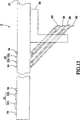
Die Signalübertragungsstruktur für einen Hochfrequenz-Test der vorliegenden Erfindung kann ebenfalls für ein Hochfrequenz-Differential-Signalpaar verwendet werden, um Treiber- bzw. Antrieb-ICs zu testen, die für ein Anzeigefeld angewendet werden. 13 zeigt eine Messfühlerkarte 4 vom Kragarm-Typ gemäß einer fünften Ausführungsform der vorliegenden Erfindung. Diese Ausführungsform ist zu der vorstehend erwähnten ersten Ausführungsform wesentlich ähnlich, ausgenommen, dass die Platine 35 der Messfühlerkarte 4 vom Kragarm-Typ mehrere Differential-Signalschaltungen 33 umfasst, die jeweils aus zwei Signaldrähten 331 und 332 gebildet sind, um ein Differential-Signalpaar zu übertragen und mehrere Erdungsschaltungen 34, die jeweils in einem bestimmten Abstand an zwei Seiten von jeder Differential-Signalschaltung 33 angeordnet vorliegen, um die charakteristische Impedanz der entsprechenden Differential-Signalpaare aufrechtzuerhalten. Die Signaldrähte 331 und 332 der Differential-Signalschaltungen 33 werden jeweils mit den Signalsonden 50 elektrisch verbunden. Die Erdungsschaltungen 34 werden jeweils mit den Erdungsschaltungen 60 elektrisch verbunden. Mit den vorstehend erwähnten strukturellen Merkmalen kann die Messfühlerkarte 4 vom Kragarm-Typ den charakteristischen Impedanzabgleich während der Übertragung der Differentialsignale aufrechterhalten.The signal transmission structure for a high frequency test of the present invention may also be used for a high frequency differential signal pair to test drive ICs applied to a display panel. 13 shows a sensor card 4 cantilever type according to a fifth embodiment of the present invention. This embodiment is substantially similar to the first embodiment mentioned above, except that the board 35 the probe card 4 cantilever-type multiple differential signal circuits 33 includes, each consisting of two signal wires 331 and 332 are formed to transmit a differential signal pair and multiple grounding circuits 34 , each at a certain distance on two sides of each differential signal circuit 33 arranged to maintain the characteristic impedance of the respective differential signal pairs. The signal wires 331 and 332 the differential signal circuits 33 are each with the signal probes 50 electrically connected. The earthing circuits 34 are each with the grounding circuits 60 electrically connected. With the structural features mentioned above, the probe card 4 of the cantilever type maintain the characteristic impedance balance during transmission of the differential signals.
14 zeigt eine Messfühlerkarte 5 vom Kragarm-Typ gemäß einer sechsten Ausführungsform der vorliegenden Erfindung. Diese Ausführungsform ist zu der vorstehend erwähnten ersten Ausführungsform wesentlich ähnlich, ausgenommen, dass die Platine 37 und die Signalsonden 57 für eine Ausgabe eines Testsignals und den/die Rückfluss bzw. Erwiderung eines entsprechend erhaltenen bzw. resultierenden Abtastsignals unterschiedliche Übertragungswege bereitstellen, was eine Interferenz zwischen Testsignal und resultierendem Signal verhindert. 14 shows a sensor card 5 cantilever type according to a sixth embodiment of the present invention. This embodiment is substantially similar to the first embodiment mentioned above, except that the board 37 and the signal probes 57 provide different transmission paths for output of a test signal and the return of a correspondingly obtained or resulting sampling signal, which prevents interference between the test signal and the resulting signal.
Die Platine 37 weist darauf mehrere angeordnete Signalschaltungen 36 auf. Jede Signalschaltung 36 umfasst einen Treiber- bzw. Messsignalführungs- bzw. Treiberdraht 361 und einen Abtastdraht 362. Der Treiberdraht 361 ist geeignet, Testbedingungen von der Testmaschine zu der entsprechenden elektronischen Einrichtung in der Testprobe zu übertragen. Der Abtastdraht 362 ist geeignet, ein Abtastsignal eines entsprechenden Testergebnisses von einer entsprechenden elektronischen Einrichtung in der Testprobe zu der Testmaschine zu übertragen. Weiterhin wird mindestens eine Erdungsschaltung 32 jeweils benachbart bzw. angrenzend zu dem Treiberdraht 361 und dem Abtastdraht 362 angeordnet, um die charakteristische Impedanz des Signalweges aufrechtzuerhalten.The board 37 has a plurality of arranged signal circuits 36 on. Every signal circuit 36 includes a driver signal wire 361 and a sensing wire 362 , The driver wire 361 is suitable for transferring test conditions from the test machine to the corresponding electronic device in the test sample. The sensing wire 362 is adapted to transmit a sample signal of a corresponding test result from a corresponding electronic device in the test sample to the test machine. Furthermore, at least one earthing circuit 32 each adjacent to or adjacent to the driver wire 361 and the sensing wire 362 arranged to maintain the characteristic impedance of the signal path.
In 14 und 15 umfasst jede Signalsonde 57 einen metallischen Stift 51 und zwei Leitungsdrähte, namentlich, einen ersten Leitungsdraht 56 und einen zweiten Leitungsdraht 52, die jeweils an dem metallischen Stift 51 angeordnet vorliegen. Strukturell gleich wie die vorstehend erwähnten Leitungsdrähte 52 umfasst der erste Leitungsdraht 56 eine metallische Leitung 560 und eine isolierte Schicht 561, die die metallische Leitung 560 koaxial umgibt. Die zwei abgewandten Enden der metallischen Leitung 560 sind jeweils mit dem metallischen Stift 51 und dem assoziierten Abtastdraht 362 elektrisch verbunden. Der zweite Leitungsdraht 52 ist mit der assoziierten Erdungsschaltung 32 elektrisch verbunden. Der metallische Stift 51 liegt mit dem assoziierten Treiberdraht 361 elektrisch verbunden vor. Weiterhin wird eine Erdungssonde 60 jeweils nahe jeder Signalsonde 57 angeordnet und mit einem bestimmten Abstand von der assoziierten Signalsonde 57 getrennt gehalten.In 14 and 15 includes each signal probe 57 a metallic pin 51 and two lead wires, namely, a first lead wire 56 and a second conductor wire 52 , each on the metallic pin 51 arranged present. Structurally the same as the above-mentioned lead wires 52 includes the first conductor wire 56 a metallic pipe 560 and an isolated layer 561 that the metallic wire 560 Coaxially surrounds. The two opposite ends of the metallic pipe 560 are each with the metallic pin 51 and the associated sensing wire 362 electrically connected. The second conductor wire 52 is with the associated ground circuit 32 electrically connected. The metallic pen 51 lies with the associated driver wire 361 electrically connected before. Furthermore, a ground probe 60 each near each signal probe 57 arranged and at a certain distance from the associated signal probe 57 kept separate.
Folglich gibt der Treiberdraht 361 von jeder Signalschaltung 36 ein Testzustandssignal von der Testmaschine an den assoziierten metallischen Stift 51 aus und der assoziierte erste Leitungsdraht 56 und der Abtastdraht 362 von jeder Signalschaltung 36 stellt einen Signalweg bereit, um das entsprechende Resultantensignal von der Testprobe an die Testmaschine zu empfangen. Da der Treiberdraht 361 und der Abtastdraht 362 von jeder Signalschaltung 36 und dem assoziierten metallischen Stift 51 und dem ersten Führungsdraht 56 von jeder Signalsonde 57 mit der Anordnung der assoziierten Erdungsschaltung 32 und dem assoziierten zweiten Leitungsdraht 52 und der assoziierten Erdungssonde 60 zusammenpassen, hält die Messfühlerkarte 5 vom Kragarm-Typ dieser sechsten Ausführungsform die charakteristische Impedanz für die Übertragung von Hochfrequenz-Signalen aufrecht und verhindert zwischen dem Testsignal und dem Abtastsignal eine Übersprech- bzw. Crosstalk-Interferenz. Folglich weist die Messfühlerkarte 5 vom Kragarm-Typ dieser sechsten Ausführungsform eine bessere Hochfrequenz-Testqualität auf.Consequently, the driver wire gives 361 from each signal circuit 36 a test condition signal from the test machine to the associated metallic pin 51 out and the associated first conductor wire 56 and the sensing wire 362 from each signal circuit 36 provides a signal path to receive the corresponding resultant signal from the test sample to the test machine. Because the driver wire 361 and the sensing wire 362 from each signal circuit 36 and the associated metallic pin 51 and the first guide wire 56 from each signal probe 57 with the arrangement of the associated ground circuit 32 and the associated second conductor wire 52 and the associated ground probe 60 match, holds the probe card 5 cantilever type of this sixth embodiment maintains the characteristic impedance for the transmission of high-frequency signals and prevents crosstalk interference between the test signal and the sampling signal. Consequently, the probe card points 5 cantilever-type of this sixth embodiment, a better high frequency test quality.
Ein zusätzlicher zweiter Leitungsdraht 52 kann jeder Signalsonde 57 hinzugefügt werden, um einen optimalen charakteristischen Impedanzabgleich bereitzustellen. 16 stellt eine Querschnittsansicht einer Signalsonde 58 gemäß einer siebten Ausführungsform der vorliegenden Erfindung dar. Gemäß dieser Ausführungsform umfasst die Signalsonde 58 einen metallischen Stift 51, einen ersten Leitungsdraht 56 und zwei zweite Leitungsdrähte 52, die jeweils zwischen dem metallischen Stift 51 und dem ersten Leitungsdraht 56 an zwei Seiten angeordnet sind. Die Signalsonde 58 gemäß dieser siebten Ausführungsform beseitigt eine Crosstalk-Interferenz zwischen dem Testsignal und dem Abtastsignal und eine Interferenz mit anderen Testsignalen wirksam und folglich weist die Signalsonde 58 eine hervorragende Übertragungsqualität eines Hochfrequenzsignals auf.An additional second conductor wire 52 can every signal probe 57 may be added to provide optimal characteristic impedance matching. 16 Fig. 3 is a cross-sectional view of a signal probe 58 according to a seventh embodiment of the present invention. According to this embodiment, the signal probe comprises 58 a metallic pin 51 , a first conductor wire 56 and two second wires 52 , each between the metallic pin 51 and the first conductor wire 56 arranged on two sides. The signal probe 58 According to this seventh embodiment, crosstalk interference between the test signal and the strobe signal effectively eliminates interference with other test signals, and thus rejects the signal probe 58 excellent transmission quality of a high-frequency signal.
Um die Größe bzw. das Maß von einer Signalsonde zu verringern, stellt die Erfindung eine in 17 gezeigte, achte Ausführungsform bereit. Wie dargestellt, umfasst jede Signalsonde 59 der Messfühlerkarte 6 vom Kragarm-Typ gemäß der achten Ausführungsform der vorliegenden Erfindung einen metallischen Stift 51 und einen ersten Leitungsdraht 56. Weiterhin wird mindestens eine Erdungssonde 60 nahe jeder Signalsonde 59 angeordnet, um die charakteristische Impedanz der assoziierten Signalsonde 59 aufrechtzuerhalten. Gemäß dieser Ausführungsform werden zwei Erdungssonden 60 an jeder der zwei abgewandten Seiten relativ zu dem metallischen Stift 51 und dem ersten Leitungsdraht 56 von jeder Signalsonde 59 angeordnet, um die charakteristische Impedanz aufrechtzuerhalten, die mit dem Testsignal und dem Abtastsignal zusammenpasst bzw. abgeglichen vorliegt und um eine Interferenz mit anderen Testsignalen zu verhindern, wodurch eine hervorragende Übertragungsqualität eines Hochfrequenzsignals erhalten wird.To reduce the size or dimension of a signal probe, the invention provides a 17 shown eighth embodiment. As illustrated, each signal probe includes 59 the probe card 6 cantilever type according to the eighth embodiment of the present invention, a metallic pin 51 and a first conductor wire 56 , Furthermore, at least one earthing probe 60 near each signal probe 59 arranged to the characteristic impedance of the associated signal probe 59 maintain. According to this embodiment, two ground probes 60 at each of the two opposite sides relative to the metallic pin 51 and the first conductor wire 56 from each signal probe 59 arranged to maintain the characteristic impedance matched with the test signal and the sampling signal, and to prevent interference with other test signals, thereby obtaining excellent transmission quality of a high-frequency signal.