CN217459643U - Wafer electroplating equipment with wafer capable of being washed - Google Patents
Wafer electroplating equipment with wafer capable of being washed Download PDFInfo
- Publication number
- CN217459643U CN217459643U CN202123456467.1U CN202123456467U CN217459643U CN 217459643 U CN217459643 U CN 217459643U CN 202123456467 U CN202123456467 U CN 202123456467U CN 217459643 U CN217459643 U CN 217459643U
- Authority
- CN
- China
- Prior art keywords
- wafer
- plate
- connecting plate
- block
- fixedly connected
- Prior art date
- Legal status (The legal status is an assumption and is not a legal conclusion. Google has not performed a legal analysis and makes no representation as to the accuracy of the status listed.)
- Active
Links
- 238000009713 electroplating Methods 0.000 title claims abstract description 47
- 230000007246 mechanism Effects 0.000 claims abstract description 39
- 238000005406 washing Methods 0.000 claims abstract description 27
- 238000011010 flushing procedure Methods 0.000 claims abstract description 15
- 239000007921 spray Substances 0.000 claims abstract description 13
- 238000005507 spraying Methods 0.000 claims abstract description 4
- XLYOFNOQVPJJNP-UHFFFAOYSA-N water Substances O XLYOFNOQVPJJNP-UHFFFAOYSA-N 0.000 claims abstract description 4
- 238000001179 sorption measurement Methods 0.000 claims description 12
- 238000007747 plating Methods 0.000 claims description 10
- 238000003825 pressing Methods 0.000 claims description 3
- 230000008878 coupling Effects 0.000 claims 5
- 238000010168 coupling process Methods 0.000 claims 5
- 238000005859 coupling reaction Methods 0.000 claims 5
- 239000012535 impurity Substances 0.000 abstract description 11
- 239000013078 crystal Substances 0.000 description 10
- 239000000463 material Substances 0.000 description 6
- 238000004140 cleaning Methods 0.000 description 4
- 241000272525 Anas platyrhynchos Species 0.000 description 3
- 238000001125 extrusion Methods 0.000 description 2
- 230000003044 adaptive effect Effects 0.000 description 1
- 238000005253 cladding Methods 0.000 description 1
- 230000000052 comparative effect Effects 0.000 description 1
- 230000007812 deficiency Effects 0.000 description 1
- 238000000034 method Methods 0.000 description 1
Images


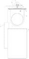


Landscapes
- Container, Conveyance, Adherence, Positioning, Of Wafer (AREA)
Abstract
The utility model relates to the field of wafer processing, in particular to wafer electroplating equipment with a wafer capable of being washed, which comprises a cabinet body, wherein a washing spray pipe is fixedly connected on the inner side wall of a washing tank, the end surface of the washing spray pipe is flush with the inner side wall of the washing tank, and the water spraying direction of a washing spray head is obliquely arranged downwards; the actuating mechanism is used for taking the wafer disc out of the electroplating bath and putting the wafer disc into the flushing tank; the wafer is slowly placed in the electroplating bath through the execution mechanism, after the wafer is electroplated, the wafer disc is slowly lifted through the execution mechanism and is slowly placed in the flushing tank, so that the wafer is directly flushed and cleaned after being electroplated, impurities on the surface of the wafer disc are timely cleaned, and then the wafer disc is transported to a designated place through the transfer device; the wafer electroplating equipment enables the wafer tray after electroplating to be directly washed and cleaned, avoids the occurrence of friction phenomenon during transportation through the transfer device, and ensures the quality of the wafer tray.
Description
Technical Field
The utility model relates to a wafer processing field specifically is wafer electroplating equipment that wafer can wash.
Background
Wafer electroplating device is used for plating one deck cladding material on the wafer disc, and after electroplating, need put into cleaning equipment, wash away its surperficial many impurity, prevent that impurity from influencing the use of wafer, wafer electroplating device now, the function is single, after wafer electroplating, through transfer device, transport it to cleaning equipment in, then clean its surperficial impurity, in the transportation process, the wafer receives the vibration, wafer surface and impurity take place the friction, influence wafer surface quality, for this reason, just wash clear wafer electroplating device after electroplating through designing one kind.
SUMMERY OF THE UTILITY MODEL
In order to make up the deficiency of the prior art, the utility model provides a wafer electroplating device with wafer flushing function.
The utility model provides a technical scheme that its technical problem adopted is: the wafer electroplating equipment with the wafer capable of being washed comprises a cabinet body, wherein the upper end surface of the cabinet body is provided with an electroplating bath and a washing tank, and the rear end surface of the cabinet body is provided with an actuating mechanism; the electroplating bath is filled with electroplating solution, a washing spray pipe is arranged in the washing tank and fixedly connected to the inner side wall of the washing tank, the end face of the washing spray pipe is flush with the inner side wall of the washing tank, and the water spraying direction of the washing spray head is obliquely arranged downwards; the actuating mechanism is used for taking the wafer disc out of the electroplating bath and putting the wafer disc into the flushing tank; the wafer is slowly placed in the electroplating bath through the execution mechanism, after the wafer is electroplated, the wafer disc is slowly lifted through the execution mechanism and is slowly placed in the flushing bath, so that the wafer is directly flushed and cleaned after being electroplated, impurities on the surface of the wafer disc are timely cleaned, and then the wafer disc is transported to a designated place through the transfer device; the wafer electroplating equipment enables the wafer tray after electroplating to be directly washed and cleaned, avoids the occurrence of friction phenomenon during transportation through the transfer device, and ensures the quality of the wafer tray.
Preferably, the actuating mechanism comprises an electric telescopic rod, a supporting plate, a motor, a screw rod, a sliding block and an adsorption mechanism; the electric telescopic rod is fixedly connected to the rear end face of the cabinet body, the upper end of the electric telescopic rod is fixedly connected with the supporting plate, one end of the supporting plate is fixedly connected with the motor, the output end of the motor is fixedly connected with the lead screw, the lead screw penetrates through the sliding block, the lower end of the sliding block penetrates through the guide groove formed in the supporting plate and is fixedly connected with the adsorption mechanism, and the adsorption mechanism is used for adsorbing and fixing the wafer disc; the supporting plate is driven to move up and down through the electric telescopic rod, so that the up-and-down movement of the crystal round plate is realized, and the motor drives the sliding block to move through the lead screw, so that the horizontal movement of the crystal round plate is realized.
Preferably, the adsorption mechanism comprises a connecting plate, a first magnetic plate, a second magnetic plate, a connecting plate and a wafer disc placing plate; the middle position of the upper plate surface of the connecting plate is fixedly connected with the lower end of the sliding block, the lower plate surface of the connecting plate is provided with a strip-shaped groove, the inner top surface of the groove is fixedly connected with a first magnetic plate, the first magnetic plate adsorbs a second magnetic plate, the second magnetic plate is fixedly connected with a connecting plate, the connecting plate is embedded into the groove, and the lower plate surface of the connecting plate is fixedly connected with a wafer disc placing plate; the upper end embedding that the board was placed to brilliant disc is in the recess, and No. two magnetic sheets adsorb on a magnetic sheet simultaneously, realizes that the wafer dish places the fixed of board this moment, realizes that the brilliant disc places quick material loading and the unloading of board, simple structure, easily operation.
Preferably, the two ends of the connecting plate are provided with clamping mechanisms; the clamping mechanism comprises a spring, a push block, a push rod and a wedge-shaped plate; cavities are formed in two ends of each connecting plate, a first hole is formed in the upper plate surface of each connecting plate, a second hole is formed in the lower plate surface of the end portion of each connecting plate, one end of each push rod is located in the first hole, the other end of each push rod is located in the second hole, the vertical end surface of the other end of each push rod is connected into the cavity through a spring, a right-angled clamping block is fixedly connected to the other end of each push rod, the clamping blocks are attached and extruded at two ends of each connecting plate, a push block is fixedly connected to one end of each push rod, and each push block is slidably connected to the upper plate surface of each connecting plate; the wedge-shaped blocks are symmetrically and fixedly connected with two ends of the supporting plate; when the connection plate moves to the other end of the supporting plate, the wedge-shaped block extrudes the push block, the push block moves towards the end part direction of the connection plate along the first hole sliding hole, meanwhile, the push block drives the push rod to extrude the spring, the other end of the push rod drives the clamping block to be far away from the disc to place the plate, the clamping block does not extrude the wafer disc to place the plate any more, when the other end of the supporting plate is far away from the connection plate, the push block, the push rod and the clamping block restore to the initial position, the push rod drives the clamping block to extrude on the wafer disc to place the plate under the elastic action of the spring, the wafer disc is placed to clamp and fix the plate once more, and firmness and stability between the wafer disc and the connection plate are improved.
Preferably, the end face of the clamping block is provided with a contact which is arranged obliquely upwards, and the end part of the connecting plate is provided with a clamping groove which is adaptive to the shape of the contact; the clamp splice extrusion is on the board is placed to the wafer dish, and the contact embedding is in the draw-in groove simultaneously to and the contact tip upwards sets up to the slope, places the board with the wafer dish and upwards pushes up, improves the wafer dish and places stability and fastness between board and the linkage plate.
Preferably, a support block is arranged below the clamping block and fixedly connected with the clamping block, and an inclined plane is arranged on the upper surface of the support block; through the supporting block and the inclined plane arranged on the supporting block, when the supporting block is close to the wafer disc for placing the plate, the supporting block supports the wafer disc, and meanwhile, the inclined plane is obliquely and upwards extruded, so that the stability between the wafer disc placing plate and the connecting plate is improved again.
Preferably, the lower plate surface of the supporting plate is symmetrically provided with pressing type buzzers, the buzzers are close to the motor, and the buzzers are symmetrically and fixedly connected to two sides of the guide groove; after the crystal disc is taken out of the flushing tank, the crystal disc moves towards the direction of the motor through the actuating mechanism, the wedge blocks extrude the push blocks, the clamping blocks are separated from the crystal disc to place the plate, meanwhile, the connecting plate extrudes the buzzer, the buzzer sends out alarm sound, the working principle of the buzzer is the same as that of the sound-making working principle of the rubber duck extrusion, the alarm sound is sent out, and an operator is warned that the crystal disc is flushed and cleaned.
Preferably, the opposite side walls of the two push blocks are provided with rotating grooves, rotating rollers are arranged in the rotating grooves, the outer rings of the rotating rollers protrude out of the surfaces of the push blocks, and the rotating rollers are rotatably connected in the rotating grooves; the wedge block is extruded on the roller, so that the relative movement smoothness between the wedge block and the push block is improved.
The utility model discloses an useful part lies in:
1. the wafer is slowly placed in the electroplating bath through the execution mechanism, after the wafer is electroplated, the wafer disc is slowly lifted through the execution mechanism and is slowly placed in the flushing bath, so that the wafer is directly flushed and cleaned after being electroplated, impurities on the surface of the wafer disc are timely cleaned, and then the wafer disc is transported to a designated place through the transfer device; the wafer electroplating equipment enables the electroplated wafer tray to be directly washed and cleaned, so that the friction phenomenon is avoided when the wafer tray is transported by the transfer device, and the quality of the wafer tray is ensured;
2. the upper end embedding that the board was placed to brilliant disc is in the recess, and No. two magnetic sheets adsorb on a magnetic sheet simultaneously, realizes that the wafer dish places the fixed of board this moment, realizes that the brilliant disc places quick material loading and the unloading of board, simple structure, easily operation.
Drawings
In order to more clearly illustrate the embodiments of the present invention or the technical solutions in the prior art, the drawings needed to be used in the description of the embodiments or the prior art will be briefly described below, it is obvious that the drawings in the following description are only some embodiments of the present invention, and for those skilled in the art, other drawings can be obtained according to the drawings without inventive exercise.
FIG. 1 is a first perspective view of a wafer electroplating apparatus according to the present invention;
FIG. 2 is a second perspective view of the middle wafer electroplating apparatus of the present invention
FIG. 3 is an enlarged view of a portion of FIG. 2 at A;
FIG. 4 is a cross-sectional view of the wafer electroplating apparatus of the present invention;
FIG. 5 is a partial enlarged view of the portion B in FIG. 4;
fig. 6 is a matching view of the wedge-shaped block pushing block of the present invention.
In the figure: the device comprises a cabinet body 1, an electroplating bath 2, a flushing tank 3, an electric telescopic rod 4, a supporting plate 5, a motor 6, a screw rod 7, a sliding block 8, a guide groove 9, a connecting plate 10, a first magnetic plate 11, a second magnetic plate 12, a connecting plate 13, a wafer disc placing plate 14, a groove 15, a spring 16, a push block 17, a push rod 18, a wedge block 19, a first hole 20, a second hole 21, a clamping block 22, a contact 23, a clamping groove 24, a supporting block 25, a buzzer 26, a rotating roller 27 and a guide block 28.
Detailed Description
The technical solutions in the embodiments of the present invention will be described clearly and completely with reference to the accompanying drawings in the embodiments of the present invention, and it is obvious that the described embodiments are only some embodiments of the present invention, not all embodiments. Based on the embodiments of the present invention, all other embodiments obtained by a person skilled in the art without creative efforts belong to the protection scope of the present invention.
The first embodiment is as follows:
referring to fig. 1-6, the wafer-washable wafer electroplating device comprises a cabinet body 1, wherein an electroplating bath 2 and a washing tank 3 are arranged on the upper end surface of the cabinet body 1, and an actuating mechanism is arranged on the rear end surface of the cabinet body 1; the electroplating bath 2 is internally provided with electroplating solution, a washing spray pipe is arranged in the washing tank 3 and is fixedly connected to the inner side wall of the washing tank 3, the end surface of the washing spray pipe is flush with the inner side wall of the washing tank 3, and the water spraying direction of the washing spray head is obliquely arranged downwards; the actuating mechanism is used for taking the wafer disc out of the electroplating bath 2 and putting the wafer disc into the flushing tank 3; the wafer electroplating equipment is used for plating a layer of plating layer on a wafer disc, and after electroplating, the wafer electroplating equipment needs to be placed into cleaning equipment to clean multiple impurities on the surface of the wafer, so that the impurities are prevented from affecting the use of the wafer; the wafer is slowly placed in the electroplating bath 2 through the execution mechanism, after the wafer is electroplated, the wafer disc is slowly lifted through the execution mechanism and is slowly placed in the flushing tank 3, so that the wafer is directly flushed and cleaned after being electroplated, impurities on the surface of the wafer disc are timely cleaned, and then the wafer disc is transported to a designated place through the transfer device; the wafer electroplating equipment enables the wafer tray after electroplating to be directly washed and cleaned, avoids the occurrence of friction phenomenon during transportation through the transfer device, and ensures the quality of the wafer tray.
The actuating mechanism comprises an electric telescopic rod 4, a supporting plate 5, a motor 6, a screw rod 7, a sliding block 8 and an adsorption mechanism; the electric telescopic rod 4 is fixedly connected to the rear end face of the cabinet body 1, the upper end of the electric telescopic rod 4 is fixedly connected with the supporting plate 5, one end of the supporting plate 5 is fixedly connected with the motor 6, the output end of the motor 6 is fixedly connected with the lead screw 7, the lead screw 7 penetrates through the sliding block 8, the lower end of the sliding block 8 penetrates through the guide groove 9 formed in the supporting plate 5 and is fixedly connected with the adsorption mechanism, and the adsorption mechanism is used for adsorbing and fixing the wafer; the supporting plate 5 is driven to move up and down through the electric telescopic rod 4, so that the up and down movement of the crystal disc is realized, and the motor 6 drives the sliding block 8 to move through the screw rod 7, so that the horizontal movement of the crystal disc is realized.
The adsorption mechanism comprises a connecting plate 10, a first magnetic plate 11, a second magnetic plate 12, a connecting plate 13 and a wafer disc placing plate 14; the middle position of the upper plate surface of the connecting plate 10 is fixedly connected with the lower end of the sliding block 8, the lower plate surface of the connecting plate 10 is provided with a strip-shaped groove 15, the inner top surface of the groove 15 is fixedly connected with a first magnetic plate 11, the first magnetic plate 11 adsorbs a second magnetic plate 12, the second magnetic plate 12 is fixedly connected with a connecting plate 13, the connecting plate 13 is embedded into the groove 15, and the lower plate surface of the connecting plate 13 is fixedly connected with a wafer disc placing plate 14; the upper end embedding that board 14 was placed to brilliant disc is in recess 15, and No. two magnetic sheets 12 adsorb simultaneously on magnetic sheet 11, realizes that the wafer dish is placed board 14's fixed this moment, realizes that the brilliant disc is placed board 14's quick material loading and unloading, simple structure, easily operation.
Two ends of the connecting plate 13 are provided with clamping mechanisms; the clamping mechanism comprises a spring 16, a push block 17, a push rod 18 and a wedge block 19; cavities are formed in two ends of the connecting plate 13, a first hole 20 is formed in the upper plate surface of the connecting plate 13, a second hole 21 is formed in the lower plate surface of the end portion of the connecting plate 13, one end of a push rod 18 is located in the first hole 20, the other end of the push rod 18 is located in the second hole 21, the vertical end surface of the other end of the push rod 18 is connected into the cavity through a spring 16, a right-angled clamping block 22 is fixedly connected to the other end of the push rod 18, the clamping block 22 is attached and extruded to two ends of the connecting plate 13, one end of the push rod 18 is fixedly connected with a push block 17, and the push block 17 is slidably connected to the upper plate surface of the connecting plate 13; the wedge-shaped blocks 19 are symmetrically and fixedly connected with two ends of the supporting plate 5; when the connecting plate 13 moves to the other end of the supporting plate 5, the wedge block 19 extrudes the push block 17, the push block 17 moves towards the end part of the connecting plate 13 along the first hole 20, meanwhile, the push block 17 drives the push rod 18 to extrude the spring 16, the other end of the push rod 18 drives the clamping block 22 to be far away from the disc placing plate, at the moment, the clamping block 22 does not extrude the wafer disc placing plate 14 any more, when the connecting plate 13 is far away from the other end of the supporting plate 5, the push block 17, the push rod 18 and the clamping block 22 recover to the initial positions, the push rod 18 drives the clamping block 22 to extrude on the wafer disc placing plate 14 under the elastic force action of the spring 16, the wafer disc placing plate 14 is clamped and fixed again, and the firmness and the stability between the wafer disc placing plate 14 and the connecting plate 13 are improved.
The end face of the clamping block 22 is provided with a contact 23, the contact 23 is arranged obliquely upwards, the end part of the connecting plate 13 is provided with a clamping groove 24, and the clamping groove 24 is matched with the contact 23 in shape; the clamping blocks 22 are extruded on the wafer disc placing plate 14, meanwhile, the contact 23 is embedded in the clamping groove 24, the end part of the contact 23 is obliquely arranged upwards, the wafer disc placing plate 14 is upwards pushed, and the stability and firmness between the wafer disc placing plate 14 and the connecting plate 13 are improved.
A support block 25 is arranged below the clamping block 22, the support block 25 is fixedly connected with the clamping block 22, and an inclined plane is arranged on the upper surface of the support block 25; through the supporting block 25 and the inclined plane arranged on the supporting block 25, when the supporting block 25 is close to the wafer disc placing plate 14, the supporting block 25 supports the wafer disc placing plate, and meanwhile, the inclined plane is obliquely and upwards extruded, so that the stability between the wafer disc placing plate 14 and the connecting plate 13 is improved again.
The lower plate surface of the supporting plate 5 is symmetrically provided with pressing type buzzers 26, the buzzers 26 are close to the motor 6, and the buzzers 26 are symmetrically and fixedly connected to two sides of the guide groove 9; after the wafer disc is taken out of the flushing tank 3, the wafer disc moves towards the motor 6 through the actuating mechanism, the wedge block 19 extrudes the push block 17, the clamping block 22 is separated from the wafer disc placing plate 14, meanwhile, the connecting plate 13 extrudes the buzzer 26, the buzzer 26 sends out alarm sound, the working principle of the buzzer 26 is the same as that of the rubber duck, the alarm sound is sent out, and an operator is warned that the wafer disc is flushed and cleaned.
The opposite side walls of the two push blocks 17 are provided with rotating grooves, rotating rollers 27 are arranged in the rotating grooves, the outer rings of the rotating rollers 27 protrude out of the surfaces of the push blocks 17, and the rotating rollers 27 are rotatably connected in the rotating grooves; the wedge block 19 is pressed on the roller 27, and relative movement smoothness between the wedge block 19 and the push block 17 is improved.
Example two:
referring to fig. 5, comparative example one, as another implementation manner of the present invention, the guide blocks 28 are symmetrically disposed at two ends of the lower plate of the first magnetic plate 11, and the wafer tray placing plate 14 is conveniently placed at the middle position of the first magnetic plate 11 through the guide blocks 28, so that the first magnetic plate 11 and the second magnetic plate 12 are completely adsorbed together.
The working principle is as follows: the wafer is slowly placed in the electroplating bath 2 through the execution mechanism, after the wafer is electroplated, the wafer disc is slowly lifted through the execution mechanism and is slowly placed in the flushing tank 3, so that the wafer is directly flushed and cleaned after being electroplated, impurities on the surface of the wafer disc are timely cleaned, and then the wafer disc is transported to a designated place through the transfer device; the wafer electroplating equipment enables the electroplated wafer tray to be directly washed and cleaned, so that the friction phenomenon is avoided when the wafer tray is transported by the transfer device, and the quality of the wafer tray is ensured;
the supporting plate 5 is driven to move up and down through the electric telescopic rod 4, so that the crystal round plate can move up and down, the motor 6 drives the sliding block 8 to move through the screw rod 7, and the crystal round plate can move in the horizontal direction;
the upper end of the wafer disc placing plate 14 is embedded into the groove 15, and the second magnetic plate 12 is adsorbed on the first magnetic plate 11, so that the wafer disc placing plate 14 is fixed, the wafer disc placing plate 14 is rapidly fed and discharged, the structure is simple, and the operation is easy;
when the connecting plate 13 moves to the other end of the supporting plate 5, the wedge-shaped block 19 extrudes the push block 17, the push block 17 moves towards the end part of the connecting plate 13 along the sliding hole of the first hole 20, meanwhile, the push block 17 drives the push rod 18 to extrude the spring 16, the other end of the push rod 18 drives the clamping block 22 to be far away from the disc placing plate, at the moment, the clamping block 22 does not extrude the wafer disc placing plate 14 any more, when the connecting plate 13 is far away from the other end of the supporting plate 5, the push block 17, the push rod 18 and the clamping block 22 recover the initial positions, the push rod 18 drives the clamping block 22 to extrude on the wafer disc placing plate 14 under the elastic force of the spring 16, the wafer disc placing plate 14 is clamped and fixed again, and the firmness and the stability between the wafer disc placing plate 14 and the connecting plate 13 are improved;
the clamping blocks 22 are extruded on the wafer disc placing plate 14, the contacts 23 are embedded in the clamping grooves 24, the end parts of the contacts 23 are arranged obliquely upwards, the wafer disc placing plate 14 is pushed upwards, and the stability and firmness between the wafer disc placing plate 14 and the connecting plates 13 are improved;
through the supporting block 25 and the inclined plane arranged on the supporting block 25, when the supporting block 25 is close to the wafer disc placing plate 14, the supporting block 25 supports the wafer disc placing plate, and meanwhile, the inclined plane is obliquely and upwards extruded, so that the stability between the wafer disc placing plate 14 and the connecting plate 13 is improved again;
after the wafer disc is taken out of the flushing tank 3, the wafer disc moves towards the motor 6 through the actuating mechanism, the wedge block 19 extrudes the push block 17, the clamping block 22 is separated from the wafer disc placing plate 14, meanwhile, the connecting plate 13 extrudes the buzzer 26, the buzzer 26 gives an alarm sound, the working principle of the buzzer 26 is the same as that of the rubber duck which extrudes to give a sound, and the alarm sound is given to warn an operator that the flushing and cleaning of the wafer disc are finished;
the wedge block 19 is pressed against the roller 27, and the smoothness of the relative movement between the wedge block 19 and the push block 17 is improved.
In the description herein, references to the description of "one embodiment," "an example," "a specific example," etc., mean that a particular feature, structure, material, or characteristic described in connection with the embodiment or example is included in at least one embodiment or example of the invention. In this specification, the schematic representations of the terms used above do not necessarily refer to the same embodiment or example. Furthermore, the particular features, structures, materials, or characteristics described may be combined in any suitable manner in any one or more embodiments or examples.
The foregoing shows and describes the basic principles, essential features, and advantages of the invention. It will be understood by those skilled in the art that the present invention is not limited to the above embodiments, and that the foregoing embodiments and descriptions are provided only to illustrate the principles of the present invention without departing from the spirit and scope of the present invention.
Claims (8)
1. Wafer electroplating equipment that wafer can be rinsed, its characterized in that: comprises a cabinet body (1), wherein the upper end surface of the cabinet body (1) is provided with an electroplating bath (2) and a washing tank (3), and the rear end surface of the cabinet body (1) is provided with an actuating mechanism; electroplating solution is contained in the electroplating bath (2), a washing spray pipe is arranged in the washing tank (3), the washing spray pipe is fixedly connected to the inner side wall of the washing tank (3), the end face of the washing spray pipe is flush with the inner side wall of the washing tank (3), and the water spraying direction of the washing spray head is obliquely arranged downwards; the actuating mechanism is used for taking the wafer disc out of the electroplating bath (2) and putting the wafer disc into the flushing tank (3).
2. The wafer flushable wafer plating apparatus of claim 1, wherein: the actuating mechanism comprises an electric telescopic rod (4), a supporting plate (5), a motor (6), a screw rod (7), a sliding block (8) and an adsorption mechanism; electric telescopic handle (4) rigid coupling is at the rear end face of the cabinet body (1), upper end rigid coupling backup pad (5) of electric telescopic handle (4), one end rigid coupling motor (6) of backup pad (5), output rigid coupling lead screw (7) of motor (6), and lead screw (7) run through slider (8), and the lower extreme of slider (8) runs through guide way (9) of seting up on backup pad (5) to the rigid coupling adsorption apparatus constructs, and adsorption apparatus constructs and is used for adsorbing fixed brilliant disc.
3. The wafer flushable wafer plating apparatus of claim 2, wherein: the adsorption mechanism comprises a connecting plate (10), a first magnetic plate (11), a second magnetic plate (12), a connecting plate (13) and a wafer disc placing plate (14); the lower end of a sliding block (8) is fixedly connected to the middle position of the upper plate surface of the connecting plate (10), a strip-shaped groove (15) is formed in the lower plate surface of the connecting plate (10), a first magnetic plate (11) is fixedly connected to the inner top surface of the groove (15), a second magnetic plate (12) is adsorbed by the first magnetic plate (11), a connecting plate (13) is fixedly connected to the second magnetic plate (12), the connecting plate (13) is embedded into the groove (15), and a wafer plate placing plate (14) is fixedly connected to the lower plate surface of the connecting plate (13).
4. The wafer flushable wafer plating apparatus of claim 3, wherein: two ends of the connecting plate (13) are provided with clamping mechanisms; the clamping mechanism comprises a spring (16), a push block (17), a push rod (18) and a wedge-shaped block (19); cavities are formed in two ends of the connecting plate (13), a first hole (20) is formed in the upper plate surface of the connecting plate (13), a second hole (21) is formed in the lower plate surface of the end portion of the connecting plate (13), one end of a push rod (18) is located in the first hole (20), the other end of the push rod (18) is located in the second hole (21), the vertical end face of the other end of the push rod (18) is connected into the cavities through a spring (16), a right-angle-shaped clamping block (22) is fixedly connected to the other end of the push rod (18), the clamping block (22) is attached and extruded at two ends of the connecting plate (13), a pushing block (17) is fixedly connected to one end of the push rod (18), and the pushing block (17) is slidably connected to the upper plate surface of the connecting plate (13); the wedge-shaped blocks (19) are symmetrically and fixedly connected with two ends of the supporting plate (5).
5. The wafer flushable wafer plating apparatus of claim 4, wherein: the end face of the clamping block (22) is provided with a contact (23), the contact (23) is arranged obliquely upwards, the end part of the connecting plate (13) is provided with a clamping groove (24), and the clamping groove (24) is matched with the contact (23) in shape.
6. The wafer rinseable wafer plating apparatus of claim 5, wherein: a supporting block (25) is arranged below the clamping block (22), the supporting block (25) is fixedly connected with the clamping block (22), and an inclined plane is arranged on the upper surface of the supporting block (25).
7. The wafer flushable wafer plating apparatus of claim 4, wherein: the lower board surface of the supporting board (5) is symmetrically provided with pressing type buzzers (26), the buzzers (26) are close to the motor (6), and the buzzers (26) are symmetrically and fixedly connected to two sides of the guide groove (9).
8. The wafer flushable wafer plating apparatus of claim 4, wherein: two on the lateral wall that ejector pad (17) are relative open the turn trough, be equipped with in the turn trough and change roller (27), change roller (27) outer lane protrusion ejector pad (17) surface, change roller (27) and rotate and connect in the turn trough.
Priority Applications (1)
| Application Number | Priority Date | Filing Date | Title |
|---|---|---|---|
| CN202123456467.1U CN217459643U (en) | 2021-12-31 | 2021-12-31 | Wafer electroplating equipment with wafer capable of being washed |
Applications Claiming Priority (1)
| Application Number | Priority Date | Filing Date | Title |
|---|---|---|---|
| CN202123456467.1U CN217459643U (en) | 2021-12-31 | 2021-12-31 | Wafer electroplating equipment with wafer capable of being washed |
Publications (1)
| Publication Number | Publication Date |
|---|---|
| CN217459643U true CN217459643U (en) | 2022-09-20 |
Family
ID=83261613
Family Applications (1)
| Application Number | Title | Priority Date | Filing Date |
|---|---|---|---|
| CN202123456467.1U Active CN217459643U (en) | 2021-12-31 | 2021-12-31 | Wafer electroplating equipment with wafer capable of being washed |
Country Status (1)
| Country | Link |
|---|---|
| CN (1) | CN217459643U (en) |
-
2021
- 2021-12-31 CN CN202123456467.1U patent/CN217459643U/en active Active
Similar Documents
| Publication | Publication Date | Title |
|---|---|---|
| CN213275673U (en) | Positioning structure for circuit board test fixture | |
| CN119187105B (en) | A continuous lead frame ultrasonic cleaning device | |
| CN111842349A (en) | PVC tubular product belt cleaning device | |
| CN218893309U (en) | Winding mechanism for electronic wire harness | |
| CN119175245A (en) | Automatic cleaning device for silicon carbide products | |
| CN115846258A (en) | Mould cleaning device is used in production of DIY toy | |
| CN218711012U (en) | Transmission wheel supporting structure of cleaning pool for electroplating | |
| CN113458034A (en) | Mould upset cleaning equipment | |
| CN119525331A (en) | Integrated pre-filling device for special-shaped tee bending processing | |
| CN111990941B (en) | A hand wash-free squeeze-dry mop bucket kit | |
| CN210386673U (en) | Two-sided cleaning device of timber | |
| CN208002753U (en) | Flat mop burnisher with liftable washer | |
| CN111973106B (en) | A horizontally inverted mop bucket kit for squeezing water | |
| CN117425286A (en) | Integrated circuit board etching tin stripping equipment | |
| CN117225812A (en) | An ultrasonic cleaning device for a metal shaft hard chromium plating production line | |
| CN118719643B (en) | Disc inner layer plate cleaning treatment device | |
| CN209750954U (en) | Mop dewatering machine | |
| CN118744136B (en) | A touch screen glass production cleaning device | |
| CN114311058A (en) | Circuit board batch forming equipment for computer hardware research and development processing based on gear linkage | |
| CN202084522U (en) | Wafer cleaning clamp | |
| CN223145534U (en) | Thermos cup washs and uses rack | |
| CN219806105U (en) | Glass grabbing device | |
| CN223629766U (en) | A welding fixture for automotive rear side panels | |
| CN219233206U (en) | Side dust collector of application spare | |
| CN218465056U (en) | Paper film unwinding device |
Legal Events
| Date | Code | Title | Description |
|---|---|---|---|
| GR01 | Patent grant | ||
| GR01 | Patent grant |