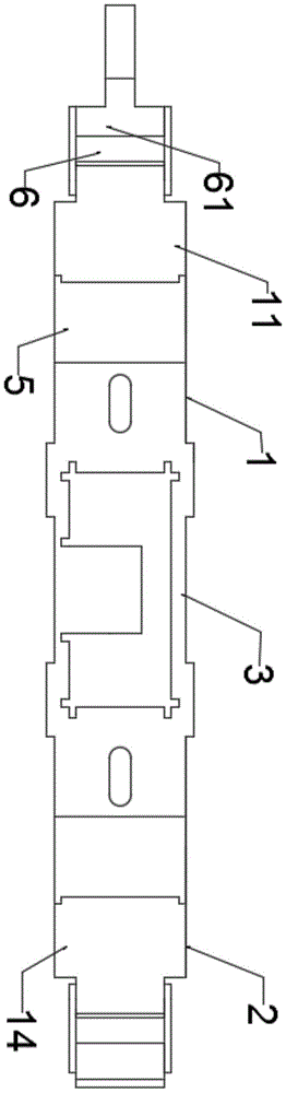
Reinforced photovoltaic bypass diode module
Technical Field
The utility model relates to the technical field of photovoltaic modules, in particular to a reinforced photovoltaic bypass diode module.
Background
The bypass diode is a diode which is reversely connected in parallel with two ends of the solar silicon cell group in the cell module, can effectively prevent the silicon cell group from being burnt due to a hot spot effect, and is an important component of the photovoltaic solar module. The bypass diode is used for preventing the solar cell from being damaged by serious heating caused by that some solar cells become loads because of being not illuminated under strong light due to shading.
The bus bar is an extension of the component welding bar, has the main function of outputting electric energy generated by the solar component, and is connected with a bypass diode in the junction box to protect the component from being damaged by hot spots. In order to avoid the damage of lightning surge to the diode.
In the prior art, firstly, a group of solar cell modules adopt a block circuitized bypass structure, and once a certain chip of the solar cell modules has a problem, the whole module is failed; secondly, 3 discrete diodes are connected in series and then are respectively welded and installed on copper sheets in the solar junction box, the heat conduction ranges of the Schottky chips have intersection, the temperature of the Schottky chips in the middle part is higher, thermal breakdown and junction box deformation and burnout are easily caused, the process is complex, the operation difficulty is high, and the waste cost is high; thirdly, the junction box is independently packaged and installed by adopting a photovoltaic module, so that the material consumption is high, the cost is high, and the processing amount is large; fourthly, when a large number of photovoltaic modules are assembled, the polarity of the photovoltaic bypass diode module is not easy to identify.
SUMMERY OF THE UTILITY MODEL
Aiming at the problems of defects and deficiencies in the prior art, the utility model provides a reinforced photovoltaic bypass diode module, which optimizes the internal structure of the photovoltaic bypass diode module, optimizes the arrangement of components, increases the number of components in the same area, realizes the maximization of single-area internal power, is easy to distinguish polarity, is convenient for subsequent processing, is convenient to install, is connected in the middle along two side lines, and reduces the cost of cables.
The technical scheme adopted by the utility model for solving the technical problems is as follows: a reinforced photovoltaic bypass diode module comprises a first photovoltaic module, a connecting frame and a second photovoltaic module which is symmetrically arranged with the first photovoltaic module; the photovoltaic module I comprises a first main board, a Schottky chip, a jumper and a second main board, wherein a chip groove is formed in the right end of the first main board, the chip groove is electrically connected with the bottom of the Schottky chip through solder paste, the top of the Schottky chip is connected with one end of the jumper through solder paste, and the other end of the jumper is electrically connected with the left end of the second main board; the first main board, the second main board and the connecting frame are manufactured through stamping.
Furthermore, the right end of the first main board and the edges of the two sides of the left end of the second main board are provided with glue locking holes.
Furthermore, the right end of the first main board and the left end of the second main board are externally provided with a package; one end of the package is provided with a bump for distinguishing polarity; the packaging material is high heat-conducting resin; the high thermal conductive resin is epoxy resin.
Furthermore, the schottky chip left side of first mainboard left end sets up the convergent current hole, the convergent current hole left end sets up the guide way that the area of converging of being convenient for passes.
Furthermore, the first main board, the second main board and the connecting frame are all made of metal copper; the first main board, the second main board and the connecting frame are coated with coatings; the coating is a tin plating coating.
Furthermore, a gap for keeping insulation is arranged between the first main board and the second main board.
The utility model has the following beneficial effects: the photovoltaic bypass diode module internal structure is optimized, the component arrangement is optimized, the number of components in the same area is increased, and the maximization of power in a single area is realized; the photovoltaic modules II are integrally and symmetrically arranged, so that the problem that one photovoltaic module is damaged and the whole module needs to be replaced due to the modularized design of a plurality of photovoltaic modules is solved, the connection cable is replaced by the junction band, the material is saved, and the cost is reduced; the problems of high material consumption and cost increase caused by the series connection of a plurality of discrete photovoltaic modules are solved, the factory cost is reduced, and the installation efficiency is improved; the packaging is provided with a bulge for distinguishing the polarity of the bypass diode; the guide groove is arranged, so that the bus bar can conveniently pass through the bus hole, the difficulty of the operation of passing the bus bar through the through hole is overcome, and the reliability of electrical connection is improved; the high-thermal-conductivity resin is adopted for packaging, so that heat can be quickly dissipated, and the heat dissipation performance is good; the mainboard is provided with the rubber locking hole, so that the packaging is tight, and the structure is firm and reliable.
Drawings
FIG. 1 is a schematic view of the structure of the present invention;
fig. 2 is a schematic structural view of a photovoltaic module according to the present invention.
Detailed Description
The following describes in detail embodiments of the present invention with reference to the drawings.
As shown in fig. 1 and 2, a reinforced photovoltaic bypass diode module includes a first photovoltaic module 1, a connecting frame 2, and a second photovoltaic module 3 symmetrically disposed with the first photovoltaic module 1; the photovoltaic module I1 comprises a first main board 11, a Schottky chip 12, a jumper sheet 13 and a second main board 14, wherein a chip groove is formed in the right end of the first main board 11 and is electrically connected with the bottom of the Schottky chip 12 through solder paste, the top of the Schottky chip 12 is connected with one end of the jumper sheet 13 through solder paste, and the other end of the jumper sheet 13 is electrically connected with the left end of the second main board 14; the first main board 11, the second main board 14 and the connecting frame 2 are made by stamping.
And rubber locking holes 4 are formed in the edges of two sides of the right end of the first main board 11 and the left end of the second main board 14.
The right end of the first main board 11 and the left end of the second main board 14 are externally provided with a package 5; a bump 51 for distinguishing polarity is provided at one end of the package 5; the packaging 5 is made of high-thermal-conductivity resin; the high thermal conductive resin is epoxy resin.
The left side of the schottky chip 12 at the left end of the first main board 11 is provided with a confluence hole 6, and the left end of the confluence hole 6 is provided with a guide groove 61 convenient for a confluence belt to pass through.
The first main board 11, the second main board 14 and the connecting frame 2 are all made of metal copper; the first main board 11, the second main board 14 and the connecting frame 2 are coated with coatings; the coating is a tin-plated coating.
A gap 7 for keeping insulation is arranged between the first main board 11 and the second main board 14.
The utility model has the following beneficial effects: the photovoltaic bypass diode module internal structure is optimized, the component arrangement is optimized, the number of components in the same area is increased, and the maximization of power in a single area is realized; the photovoltaic modules II 3 are integrally and symmetrically arranged, so that the problem that one photovoltaic module is damaged and the whole module needs to be replaced due to the blocking design of a plurality of photovoltaic modules is solved, the junction cable is replaced by the junction belt, the material is saved, and the cost is reduced; the problems of high material consumption and cost increase caused by the series connection of a plurality of discrete photovoltaic modules are solved, the factory cost is reduced, and the installation efficiency is improved; the package 5 is provided with a bump for discriminating the polarity of the bypass diode; the guide groove 61 is arranged, so that the bus bar can conveniently pass through the bus hole 6, the difficulty of the operation of passing the bus bar through a through hole is overcome, and the reliability of electrical connection is improved; the high-thermal-conductivity resin is adopted for packaging, so that heat can be quickly dissipated, and the heat dissipation performance is good; the mainboard is provided with the glue locking hole 4, so that the encapsulation is tight, and the structure is firm and reliable.
The foregoing shows and describes the general principles, essential features, and advantages of the utility model. The present invention is not limited to the above-described embodiments, which are described in the specification and illustrated only for illustrating the principle of the present invention, but various changes and modifications may be made within the scope of the present invention as claimed without departing from the spirit and scope of the present invention. The scope of the utility model is defined by the appended claims and equivalents thereof.