CN216391916U - Adapter and lighting lamp - Google Patents
Adapter and lighting lamp Download PDFInfo
- Publication number
- CN216391916U CN216391916U CN202122908584.0U CN202122908584U CN216391916U CN 216391916 U CN216391916 U CN 216391916U CN 202122908584 U CN202122908584 U CN 202122908584U CN 216391916 U CN216391916 U CN 216391916U
- Authority
- CN
- China
- Prior art keywords
- heat
- circuit board
- electronic component
- heat sink
- adapter
- Prior art date
- Legal status (The legal status is an assumption and is not a legal conclusion. Google has not performed a legal analysis and makes no representation as to the accuracy of the status listed.)
- Active
Links
Images


Abstract
The application discloses adapter and illumination lamps and lanterns belongs to illumination lamps and lanterns accessory design technical field. The disclosed adapter comprises a shell, a circuit board, a first electronic component and a first radiating fin, wherein the circuit board and the first radiating fin are arranged in the shell, the circuit board comprises a first surface and a second surface which are arranged in a back-to-back mode, the first electronic component is arranged on the first surface of the circuit board, the first radiating fin is arranged on one side of the first surface of the circuit board to dissipate heat of the first electronic component, and the first radiating fin is made of an insulating heat conduction material. The disclosed lighting fixture includes the adapter described above. Due to the arrangement, the first radiating fin is made of the insulating heat conduction material, so that the radiating effect can be ensured, and the insulating effect can be achieved, other insulating materials do not need to be additionally arranged, the thermal resistance between the first electronic component and the first radiating fin is reduced, and the radiating performance is improved; meanwhile, the number of heat transfer parts is reduced, and the later assembly process is simplified.
Description
Technical Field
The application belongs to the technical field of lighting lamp accessory design, and particularly relates to an adapter and a lighting lamp.
Background
With the rapid development of new technologies, adapters are developed toward high power density and high reliability to shorten charging time by increasing charging power. However, in order to achieve the effect of improving the power density, the power devices of the adapter are distributed in a concentrated manner, and heat generation is concentrated, which results in a high internal temperature of the adapter.
In order to realize the heat dissipation effect, in the adapter disclosed in the related art, an electronic component is arranged on the surface of the circuit board, heat generated by electrifying the electronic component is transferred to the metal heat dissipation sheet, and the metal heat dissipation sheet is provided with a mylar sheet facing one side of the circuit board, the mylar sheet has an insulation effect, and through the mylar sheet, the risk of electricity crosstalk is avoided and the requirement on the safety specification of the adapter is met. However, the mylar sheet increases the thermal resistance between the electronic component and the metal heat sink, and the overall heat dissipation performance is reduced. Moreover, the types of heat transfer components are many, and the later assembly process is more complicated.
SUMMERY OF THE UTILITY MODEL
An object of the embodiment of the application is to provide an adapter and a lighting lamp, which can solve the problems that in the related art, the insulation sheet is separately arranged, so that the thermal resistance between an electronic component and a metal radiating fin is increased, the radiating performance is reduced, the types of heat transfer components are multiple, and the assembly process is complicated.
In a first aspect, an embodiment of the present application provides an adapter, including a housing, a circuit board, a first electronic component, and a first heat sink, wherein:
the circuit board with first fin is located in the casing, the circuit board includes first face and the second face that sets up mutually, first electronic components locates the first face of circuit board, first fin is located one side of the first face of circuit board, in order to do first electronic components dispels the heat, first fin is made by insulating heat conduction material.
In a second aspect, an embodiment of the present application provides a lighting fixture, including the above adapter.
In this application embodiment, because first fin adopts insulating heat conduction material, so first fin can guarantee the heat dissipation, can play insulating effect again, does not have the cluster electric danger, has satisfied safety standard's requirement, so need not to set up other insulating material in addition again. With the arrangement, the thermal resistance between the first electronic component and the first radiating fin is reduced, and the radiating performance is improved; moreover, the number of heat transfer parts is reduced, simplifying the post assembly process.
Drawings
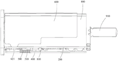
FIG. 1 is a front view of the internal structure of an adapter as disclosed in the background of the present application;
FIG. 2 is a schematic diagram of the internal structure of an adapter disclosed in the background of the present application;
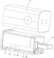
FIG. 3 is a schematic external view of an adapter disclosed in an embodiment of the present application;
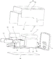
FIG. 4 is an exploded schematic view of an adapter disclosed in an embodiment of the present application;
fig. 5 is an exploded view of the adapter at another angle according to the disclosure of the present application.
Description of reference numerals:
100-a housing; 110-opening a hole;
200-a circuit board; 210-slotting;
310-a first electronic component;
320-a transformer; 321-a plug-in connector;
330-a rectifying plate; 340-a fuse; 350-thermistor; 360-capacitance;
400-a first heat sink;
500-thermally conductive connecting layer;
600-a second heat sink; 610-a first heat sink portion; 620 — a second heat sink portion; 621-a first extension;
700-heat conducting gasket; 710-a first heat conducting portion; 720-a second heat conducting portion;
800-mylar film; 810-a second extension;
910-a plug; 920-socket.
Detailed Description
The technical solutions in the embodiments of the present application will be described clearly below with reference to the drawings in the embodiments of the present application, and it is obvious that the described embodiments are some, but not all, embodiments of the present application. All other embodiments that can be derived by one of ordinary skill in the art from the embodiments given herein are intended to be within the scope of the present disclosure.
The terms first, second and the like in the description and in the claims of the present application are used for distinguishing between similar elements and not necessarily for describing a particular sequential or chronological order. It will be appreciated that the data so used may be interchanged under appropriate circumstances such that embodiments of the application may be practiced in sequences other than those illustrated or described herein, and that the terms "first," "second," and the like are generally used herein in a generic sense and do not limit the number of terms, e.g., the first term can be one or more than one.
The adapter and the lighting fixture provided in the embodiments of the present application are described in detail below with reference to the accompanying drawings through specific embodiments and application scenarios thereof.
Referring to fig. 1-5, an adapter is disclosed that includes a housing 100, a circuit board 200, a first electronic component 310, and a first heat sink 400. The housing 100 is a housing of the adapter, and is used for accommodating other components; the circuit board 200, the first heat sink 400 and the first electronic component 310 are all disposed in the housing 100, and the circuit board 200 is a support body for the first electronic component 310 and is also a carrier for the first electronic component 310 to be electrically connected.
The circuit board 200 includes a first surface and a second surface that are opposite to each other, the first surface of the circuit board 200 is provided with a first electronic component 310, and the first electronic component 310 can be electrically connected with the circuit board 200. Specifically, the first electronic component 310 can generate heat during the electrical connection process and dissipate the heat by means of the first heat sink 400. The first electronic component 310 may be fixed on the circuit board 200 by soldering, bonding, or the like, or may be detachably connected on the circuit board 200 by plugging, clipping, or the like. In this embodiment, the first electronic component 310 may be a switch tube, or may be another type of electronic component.
The first heat sink 400 is disposed at a side portion of the circuit board 200, and the first heat sink 400 is disposed at a side of the first surface of the circuit board 200, that is, the first heat sink 400 faces the first surface of the circuit board 200, so that the first heat sink 400 dissipates heat for the first electronic component 310. That is, the first heat sink 400 and the first electronic component 310 are located on the same side of the circuit board 200. Alternatively, the first heat sink 400 may be in direct contact with the first electronic component 310, or may be directly attached to the first surface of the circuit board 200, and of course, the first heat sink 400 may also be in contact with neither the first electronic component 310 nor the circuit board 200, in this case, the heat of the first electronic component 310 is transferred to the first heat sink 400 through air, in short, as long as the heat of the first electronic component 310 can be dissipated through the first heat sink 400.
The first heat sink 400 is made of an insulating and heat-conducting material, which means that the first heat sink 400 has only heat-conducting property, can receive heat transferred from the first electronic component 310, but has no electric-conducting property, and there is no problem of electric crosstalk between the first electronic component 310 and the first heat sink 400.
With the arrangement, the first heat sink 400 is made of the insulating heat-conducting material, so that the first heat sink 400 can ensure heat dissipation and also has an insulating effect, no electric cross risk exists, the requirement on the safety specification of the adapter is met, other parts with the insulating effect do not need to be additionally arranged, the thermal resistance between the first electronic component 310 and the first heat sink 400 can be reduced, and the heat dissipation performance is improved; moreover, the number of heat transfer parts is reduced, and the post assembly process is simplified.
In an alternative embodiment, a heat conductive connector is disposed between the first heat sink 400 and the circuit board 200, the heat conductive connector connects the first heat sink 400 and the first electronic component 310, and the material of the heat conductive connector is a heat conductive material. Specifically, the heat-conducting connecting member has heat-conducting performance and a connecting function, and can connect the first heat sink 400 and the first electronic component 310, and quickly transfer heat generated by the first electronic component 310 to the first heat sink 400, so as to dissipate heat.
With such an arrangement, the heat generated by the first electronic component 310 can be effectively conducted to the first heat sink 400 through the heat conductive connector, and then dissipated to the surrounding air through the first heat sink 400, so as to shorten the heat dissipation time and improve the heat dissipation efficiency.
In this embodiment, the first heat sink 400 may be a ceramic sheet, and although the ceramic material has a thermal conductivity lower than that of the metal material, the ceramic material is a relatively excellent thermal conductivity material in the insulating material, and the thermal conductivity is more excellent than that of the insulating material such as plastic and rubber. However, the first heat sink 400 is not limited to a ceramic plate, and the first heat sink 400 may also be a silicone plate or other insulating plate.
In an alternative embodiment, as shown in fig. 1, the heat conductive connector is a heat conductive connection layer 500, the heat conductive connection layer 500 is disposed on the surface of the first heat sink 400, the area of the heat conductive connection layer 500 may be smaller than the area of the side of the first heat sink 400 facing the circuit board 200, and the area of the heat conductive connection layer 500 may also be equal to the area of the side of the first heat sink 400 facing the circuit board 200. Furthermore, at least a portion of the first electronic component 310 may extend into the heat conducting connection layer 500, that is, a portion of the first electronic component 310 may extend into the heat conducting connection layer 500, or the whole first electronic component 310 may extend into the heat conducting connection layer 500.
Under the condition that the whole of the first electronic component 310 extends into the heat-conducting connection layer 500, that is, the heat-conducting connection layer 500 is laid on the first surface of the circuit board 200, the contact area between the first electronic component 310 and the heat-conducting connection layer 500 is the largest, and the heat transfer efficiency between the first electronic component 310 and the heat-conducting connection layer 500 is the highest.
With this arrangement, the heat conductive connector is layered, the contact area between the heat conductive connector and the first heat sink 400 is large, and the heat transfer efficiency between the heat conductive connector and the first heat sink 400 is improved.
In this embodiment, the heat conductive connecting member is a heat conductive adhesive, and the heat conductive connecting layer 500 is a heat conductive adhesive layer. The heat-conducting glue is heat-conducting silica gel which is formed by mixing organic silica gel serving as a main body with high polymer materials such as filling materials, heat-conducting materials and the like, and has good heat-conducting property and insulating property. Of course, the heat conductive connector is not limited to the heat conductive glue, and in other embodiments, the heat conductive connector may be heat conductive silicone grease, or may be other components with heat conductive performance and connection performance.
So set up, the bonding strength of heat-conducting glue is high, can solidify moreover, is the elastomer after the solidification, possesses certain shock resistance and anti-seismic performance.
In an alternative embodiment, the number of first electronic components 310 is at least two. In this way, the first heat sink 400 can dissipate heat for the at least two first electronic components 310.
In this embodiment, each of the first electronic components 310 is disposed on the first surface of the circuit board 200, and at least a portion of each of the first electronic components 310 extends into the thermal conductive connection layer 500.
So set up, through heat conduction connection layer 500, can be with the heat of two at least first electronic components 310 for transmitting to first fin 400 effectively, realize two at least first electronic components 310's quick heat dissipation, further promote the radiating efficiency.
In a further technical solution, as shown in fig. 4 and 5, the adapter further includes a second electronic component and a second heat sink 600, the second electronic component is disposed on the second surface of the circuit board 200, the second heat sink 600 is located on a side portion of the circuit board 200, and the second heat sink 600 is disposed on one side of the second surface of the circuit board 200, that is, the second heat sink 600 faces the second surface of the circuit board 200, so that the second heat sink 600 dissipates heat for the second electronic component, that is, the first electronic component 310 and the second electronic component are respectively located on two sides of the circuit board 200, and the second heat sink 600 and the second electronic component are located on the same side of the circuit board 200. In this embodiment, the second electronic component may be a transformer 320.
Specifically, the second heat sink 600 and the second electronic component may or may not be in direct contact, as long as the heat generated by the second electronic component during the power-on process can be transferred to the second heat sink 600, and the second heat sink 600 dissipates the heat to the ambient air.
With such an arrangement, the second heat sink 600 is utilized to dissipate heat of the second electronic component located on the second surface of the circuit board 200, so as to further improve the overall heat dissipation effect of the adapter.
Referring to fig. 2, in a direction perpendicular to the circuit board 200, a distance from the first surface of the circuit board 200 to the housing 100 is smaller than a distance from the second surface of the circuit board 200 to the housing 100, that is, the first surface of the circuit board 200 is closer to the housing 100 than the second surface of the circuit board 200, and thus, a portion of the housing 100 close to the first surface of the circuit board 200 is more vulnerable to electric shock. The first heat sink 400 is an insulating sheet, which largely prevents the possibility of electric shock of the housing 100.
In this embodiment, a mylar sheet 800 is disposed between the circuit board 200 and the second heat sink 600, the mylar sheet 800 is attached to the second heat sink 600, and the mylar sheet 800 may or may not contact the second electronic component. Specifically, mylar sheet 800 has an insulating effect, and of course, other spacers having an insulating effect may be disposed between circuit board 200 and second heat sink 600, so as to prevent second heat sink 600 from being conductive.
In the case where second heat sink 600 is a metal heat sink, there is a risk of crosstalk if second heat sink 600 contacts with a second electronic component. So set up, through mylar piece 800, keep apart second electronic components and second fin 600, avoid the string electricity hidden danger.
In an alternative embodiment, a surface of the second electronic component is provided with a thermal pad 700, the thermal pad 700 is connected to the second heat sink 600, and the thermal pad 700 may be in contact with both the surface of the second electronic component and the surface of the second heat sink 600.
So set up, through heat conduction gasket 700, can effectively transmit the heat that second electronic components sent for second fin 600, rethread second fin 600 dispels the heat to second electronic components's heat, improves heat conduction efficiency.
Specifically, the second heat sink 600 has a heat conducting property, and may be a metal heat sink or an insulating heat sink. In an alternative embodiment, mylar sheet 800 is disposed between heat-conducting spacer 700 and second heat sink 600, and mylar sheet 800 is in contact with both heat-conducting spacer 700 and second heat sink 600.
Alternatively, the thermal pad 700 includes a first thermal conduction portion 710 and a second thermal conduction portion 720, and the second heat sink 600 includes a first heat sink portion 610 and a second heat sink portion 620. The first heat conduction portion 710 is attached to a surface of the second electronic component facing away from the circuit board 200, the second heat conduction portion 720 is matched with a side surface of the second electronic component, and the second heat conduction portion 720 is located between the first heat conduction portion 710 and the circuit board 200.
The first heat conducting part 710 and the second heat conducting part 720 can be of an integrated structure or a split structure, that is, the first heat conducting part 710 and the second heat conducting part 720 are separate heat conducting gaskets 700, as long as the first heat conducting part 710 and the second heat conducting part 720 are both attached to the second electronic component, so that the heat of the second electronic component can be transferred to the first heat conducting part 710 and the second heat conducting part 720; meanwhile, the first heat dissipation part 610 is attached to the first heat conduction part 710, and the second heat dissipation part 620 is attached to the second heat conduction part 720, so that the heat of the first heat conduction part 710 is transferred to the first heat dissipation part 610, and meanwhile, the heat of the second heat conduction part 720 is transferred to the second heat dissipation part 620.
With this arrangement, the heat of the second electronic component includes two parts, wherein one part of the heat is transferred to the first heat dissipation portion 610 through the first heat conduction portion 710, and the other part of the heat is transferred to the second heat dissipation portion 620 through the second heat conduction portion 720, so that the heat transfer efficiency is improved.
In the present embodiment, as shown in fig. 4 and 5, two second heat-conducting portions 720 and two second heat-dissipating portions 620 are provided, the first heat-conducting portion 710 is located between the two second heat-conducting portions 720, and the first heat-dissipating portion 610 is located between the two second heat-dissipating portions 620. Because the second heat conduction parts 720 are in contact with the side surfaces of the second electronic component, the two second heat conduction parts 720 are located on the two sides of the second electronic component opposite to each other, and meanwhile, the two second heat dissipation parts 620 are also located on the two sides of the second electronic component opposite to each other.
Thus, the contact area between the thermal pad 700 and the second electronic component is large, the contact area between the thermal pad 700 and the second heat sink 600 is also large, the heat transfer area is increased, and the heat transfer efficiency is further improved.
In this embodiment, the surface of the mylar tab 800 facing the second electronic component is in contact with both the first heat conducting portion 710 and the second heat conducting portion 720, and the surface of the mylar tab 800 facing away from the second electronic component is in contact with both the first heat dissipating portion 610 and the second heat dissipating portion 620. That is to say, mylar sheet 800 is arranged between first heat-conducting portion 710 and first heat-dissipating portion 610, and mylar sheet 800 is also arranged between second heat-conducting portion 720 and second heat-dissipating portion 620, so that electricity leakage is prevented to a large extent, and safety in use is ensured.
Optionally, the first heat sink piece 610 and the two second heat sink pieces 620 are a unitary structure. In this way, the second electronic component is sandwiched between the two second heat conduction parts 720, and the second electronic component and the two second heat conduction parts 720 are sandwiched between the two second heat dissipation parts 620, and the second electronic component, the second heat conduction parts 720 and the second heat dissipation plate 600 are in contact in sequence, so that the second heat conduction parts 720 and the second heat dissipation plate 600 are prevented from moving in a direction perpendicular to the second heat dissipation part 620, and the mounting stability is ensured.
In an alternative embodiment, as shown in fig. 4, the second electronic component is provided with a plug 321, the circuit board 200 is provided with a jack, and the plug 321 penetrates through the jack and extends into the heat-conducting connecting layer 500. Therefore, the plug-in connection mode is adopted, the second electronic component is convenient to mount and dismount, and the maintenance is convenient.
Optionally, as shown in fig. 1-2 and 4-5, an opening and a slot 210 are formed at an edge of the circuit board 200, the second heat sink 600 is provided with a first extension portion 621, the first extension portion 621 is disposed at an edge of the second heat sink portion 620, and the first extension portion 621 extends into the opening; moreover, the mylar sheet 800 is provided with a second extending portion 810, the second extending portion 810 is arranged at the edge of the mylar sheet 800, and the second extending portion 810 extends into the slot 210 from the edge of the circuit board 200 and is in limit contact with the circuit board 200 along the direction perpendicular to the circuit board 200.
In this embodiment, the second extending portion 810 includes a protruding portion, and after the second extending portion 810 extends into the slot 210, the protruding portion is located on the first surface of the circuit board 200, and the protruding portion is in limited contact with the circuit board 200, so that the second extending portion 810 is prevented from being separated from the slot 210, and the mounting stability of the mylar sheet 800 is improved.
In a further technical solution, as shown in fig. 3 and 4, the adapter further includes a plug 910 and a socket 920, the plug 910 and the socket 920 are both disposed on the circuit board 200, wherein the socket 920 is provided with an interface, the housing 100 is provided with an opening 110, the interface is communicated with the opening 110, at least a portion of the plug 910 extends out of the housing 100, and the plug 910 and the socket 920 are both electrically connected to the circuit board 200.
In this way, the device to be charged is inserted into the interface through the opening 110, so as to electrically connect the device to be charged and the socket 920, and the plug 910 is externally connected to input commercial power, and the input commercial power is output to the socket 920 through the circuit board 200, and is finally supplied to the device to be charged.
In an alternative embodiment, as shown in fig. 4 and 5, the second electronic component includes at least one of a transformer 320, a capacitor 360, a thermistor 350, a fuse 340, and a rectifying plate 330, and at least one of the transformer 320, the rectifying plate 330, the fuse 340, the thermistor 350, and the capacitor 360 is disposed on the second surface of the circuit board 200 and electrically connected to the circuit board 200.
Specifically, the adapter may include one of the transformer 320, the rectifying plate 330, the fuse 340, the thermistor 350, and the capacitor 360, two of the five, three of the five, or four of the five. In this embodiment, the second electronic component includes a transformer 320, a capacitor 360, a thermistor 350, a fuse 340, and a rectifying plate 330, and the thermal pad 700 is disposed on the surface of the transformer 320.
Thus, heat generated by the transformer 320, the capacitor 360, the thermistor 350, the fuse 340 and the rectifying plate 330 can be dissipated by the second heat sink 600.
Specifically, the high voltage can be stepped down to a low voltage that can be directly used by the transformer 320; functions of bypass, decoupling, filtering, energy storage and the like are realized through the capacitor 360; the thermistor 350 can show different resistance values in different temperature environments, so that temperature compensation and temperature control are realized; the fuse 340 plays a role of overload protection for the circuit; the ac power is rectified by the rectifying plate 330, and the ac power can be rectified into dc power.
So set up, plug 910 connects the input commercial power, and the commercial power is high-voltage alternating current usually, exports for the direct current low-voltage current that can directly use after effect such as internal circuit rectification, vary voltage, isolation, and socket 920 supplies the equipment of waiting to charge with direct current low-voltage current.
Based on the adapter of this application, this application embodiment still discloses a lighting fixture, and the lighting fixture that discloses includes the adapter in above-mentioned embodiment.
While the present embodiments have been described with reference to the accompanying drawings, it is to be understood that the invention is not limited to the precise embodiments described above, which are meant to be illustrative and not restrictive, and that various changes may be made therein by those skilled in the art without departing from the spirit and scope of the invention as defined by the appended claims.
Claims (12)
1. An adapter, comprising a housing (100), a circuit board (200), a first electronic component (310), and a first heat sink (400), wherein:
the circuit board (200) and the first radiating fin (400) are arranged in the shell (100), the circuit board (200) comprises a first surface and a second surface which are arranged in a back-to-back mode, the first electronic component (310) is arranged on the first surface of the circuit board (200), the first radiating fin (400) is arranged on one side of the first surface of the circuit board (200) to dissipate heat of the first electronic component (310), and the first radiating fin (400) is made of insulating heat conduction materials.
2. The adapter as claimed in claim 1, characterized in that a thermally conductive connection is provided between the first heat sink (400) and the circuit board (200), the thermally conductive connection connects the first heat sink (400) and the first electronic component (310), and the thermally conductive connection is made of a thermally conductive material.
3. The adapter as claimed in claim 2, characterized in that the thermally conductive connection is a thermally conductive connection layer (500), the thermally conductive connection layer (500) being applied to the surface of the first heat sink (400), and at least part of the first electronic component (310) protruding into the thermally conductive connection layer (500).
4. The adapter as claimed in claim 1, characterized in that the number of first electronic components (310) is at least two.
5. The adapter of claim 1, further comprising a second electronic component disposed on the second side of the circuit board (200) and a second heat sink (600), the second heat sink (600) being disposed on a side of the second side of the circuit board (200) to dissipate heat from the second electronic component.
6. The adapter of claim 5, wherein the surface of the second electronic component is provided with a heat conducting gasket (700), and the heat conducting gasket (700) is connected with the second heat sink (600).
7. The adapter of claim 6, wherein the thermally conductive gasket (700) comprises a first thermally conductive portion (710) and a second thermally conductive portion (720), the second heat sink (600) comprising a first heat sink portion (610) and a second heat sink portion (620), wherein:
the first heat conduction part (710) is attached to the surface of the second electronic component, which faces away from the circuit board (200), the second heat conduction part (720) is attached to the side surface of the second electronic component, and the second heat conduction part (720) is located between the first heat conduction part (710) and the circuit board (200); the first heat dissipation portion (610) is attached to the first heat conduction portion (710), and the second heat dissipation portion (620) is attached to the second heat conduction portion (720).
8. The adapter of claim 5, wherein a mylar tab (800) is disposed between the circuit board (200) and the second heat sink (600), the mylar tab (800) being attached to the second heat sink (600).
9. The adapter of claim 1, comprising a plug (910) and a socket (920), the plug (910) and the socket (920) each being provided to the circuit board (200), wherein:
the socket (920) is provided with an interface, the shell (100) is provided with an opening (110), the interface is communicated with the opening (110), at least part of the plug (910) extends out of the shell (100), and the plug (910) and the socket (920) are electrically connected with the circuit board (200).
10. The adapter of claim 5, wherein the second electronic component comprises at least one of a transformer (320), a rectifying plate (330), a fuse (340), a thermistor (350), and a capacitor (360), and wherein at least one of the transformer (320), the rectifying plate (330), the fuse (340), the thermistor (350), and the capacitor (360) is disposed on a second side of the circuit board (200) and is electrically connected to the circuit board (200).
11. The adapter of claim 2, wherein the thermally conductive connector is a thermally conductive glue and the first heat sink (400) is a ceramic plate.
12. A lighting fixture comprising an adapter according to any one of claims 1-11.
Priority Applications (1)
| Application Number | Priority Date | Filing Date | Title |
|---|---|---|---|
| CN202122908584.0U CN216391916U (en) | 2021-11-24 | 2021-11-24 | Adapter and lighting lamp |
Applications Claiming Priority (1)
| Application Number | Priority Date | Filing Date | Title |
|---|---|---|---|
| CN202122908584.0U CN216391916U (en) | 2021-11-24 | 2021-11-24 | Adapter and lighting lamp |
Publications (1)
| Publication Number | Publication Date |
|---|---|
| CN216391916U true CN216391916U (en) | 2022-04-26 |
Family
ID=81217426
Family Applications (1)
| Application Number | Title | Priority Date | Filing Date |
|---|---|---|---|
| CN202122908584.0U Active CN216391916U (en) | 2021-11-24 | 2021-11-24 | Adapter and lighting lamp |
Country Status (1)
| Country | Link |
|---|---|
| CN (1) | CN216391916U (en) |
Cited By (1)
| Publication number | Priority date | Publication date | Assignee | Title |
|---|---|---|---|---|
| CN117479509A (en) * | 2023-12-26 | 2024-01-30 | 深圳市蓝禾技术有限公司 | Charging device |
-
2021
- 2021-11-24 CN CN202122908584.0U patent/CN216391916U/en active Active
Cited By (1)
| Publication number | Priority date | Publication date | Assignee | Title |
|---|---|---|---|---|
| CN117479509A (en) * | 2023-12-26 | 2024-01-30 | 深圳市蓝禾技术有限公司 | Charging device |
Similar Documents
| Publication | Publication Date | Title |
|---|---|---|
| CN107529312A (en) | Optical module with double-deck PCBA structures | |
| CN114916160A (en) | Power adapter | |
| CN216391916U (en) | Adapter and lighting lamp | |
| TW201121393A (en) | Heat dissipating structure of socket pins | |
| CN217388260U (en) | Charger convenient to heat dissipation | |
| CN216873721U (en) | Intelligent platform area fusion terminal | |
| CN216626417U (en) | Integrated radiator for platform area terminal | |
| CN215773989U (en) | Charging plug | |
| CN213028875U (en) | Switch shell structure capable of dissipating heat rapidly | |
| CN210866417U (en) | Battery module fast dispels heat | |
| CN211128734U (en) | Busbar capacitor assembly heat dissipation device and electric automobile driving motor controller | |
| CN112701880A (en) | Capacitor module insulation heat dissipation mode of power supply | |
| CN110690529A (en) | Battery module fast dispels heat | |
| CN218735659U (en) | Outdoor power supply device capable of quickly dissipating heat | |
| CN213044021U (en) | Ceramic radiating fin fixing mechanism | |
| CN220673728U (en) | Split type photovoltaic junction box | |
| CN216527051U (en) | Heat radiator for sealed terminal equipment | |
| CN215647962U (en) | Mobile phone heat dissipation mainboard based on copper material | |
| CN211478771U (en) | Heat abstractor and head-mounted display device | |
| CN213460174U (en) | Charging connector | |
| CN219740724U (en) | Lithium battery protection board | |
| CN220121933U (en) | Emergency power supply heat abstractor and emergency power supply | |
| CN215222807U (en) | Novel no fan industry switch heat radiation structure | |
| CN212137321U (en) | Solar charging controller | |
| US20070297142A1 (en) | Power supply apparatus having passive heat-dissipation mechanism and fabrication method thereof |
Legal Events
| Date | Code | Title | Description |
|---|---|---|---|
| GR01 | Patent grant | ||
| GR01 | Patent grant |