SUMMERY OF THE UTILITY MODEL
The purpose of the utility model is as follows: the LED driving power supply device can select different output current ranges according to the LED load condition, and dimming in the ranges can ensure that the load is not damaged.
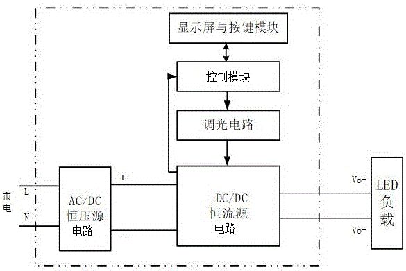
The technical scheme is as follows: the LED driving power supply device is used for supplying power to an LED load; the device comprises an AC/DC constant-voltage source circuit, a DC/DC constant-current source circuit, a dimming circuit and a control module;
the positive output end and the negative output end of the AC/DC constant-voltage source circuit are respectively butted with the positive input end and the negative input end of the DC/DC constant-current source circuit; the first signal output end to the sixth signal output end of the control module are respectively connected with the first signal input end to the sixth signal input end of the dimming circuit in a one-to-one correspondence manner, and the signal output end of the dimming circuit is in butt joint with the signal input end of the DC/DC constant current source circuit; a positive output end and a negative output end of the DC/DC constant current source circuit are respectively butted with a positive input end and a negative input end of the LED load;
the dimming circuit comprises a MOS tube Q1, a MOS tube Q2, a MOS tube Q3, a MOS tube Q4, a MOS tube Q5, a MOS tube Q6, a resistor R1, a resistor R2, a resistor R3, a resistor R4, a resistor R5, a capacitor C1 and an operational amplifier U1; the gate of the MOS transistor Q1, the gate of the MOS transistor Q2, the gate of the MOS transistor Q3, the gate of the MOS transistor Q4, the gate of the MOS transistor Q5, and the gate of the MOS transistor Q6 sequentially form a first signal input end, a second signal input end, a third signal input end, a fourth signal input end, a fifth signal input end, and a sixth signal input end of the dimming circuit;
one end of the resistor R1 is connected with an external power supply, and the other end of the resistor R1 is connected with one end of the resistor R2, the drain electrode of the MOS transistor Q3 and the drain electrode of the MOS transistor Q6; the other end of the resistor R2 is connected with one end of the resistor R3, the drain of the MOS transistor Q2 and the drain of the MOS transistor Q5; the other end of the resistor R3 is connected with one end of the resistor R4, the drain of the MOS transistor Q1 and the drain of the MOS transistor Q4; the other end of the resistor R4 is connected with the source electrode of the MOS tube Q3, the source electrode of the MOS tube Q2, the source electrode of the MOS tube Q1 and one end of the capacitor C1, and the connection point is grounded; the source electrode of the MOS transistor Q6, the source electrode of the MOS transistor Q5, the source electrode of the MOS transistor Q4 and one end of the resistor R5 are connected; the other end of the resistor R5 is connected with the other end of the capacitor C1 and the positive input end of the signal amplifier U1; the negative input end of the signal amplifier is connected with the output end of the signal amplifier, and the connection point forms the signal output end of the dimming circuit.
As a preferable aspect of the present invention, the AC/DC constant voltage power supply circuit includes a power filter M1, a diode D1, a diode D2, a diode D3, a diode D4, a diode D5, an inductor L1, a capacitor C2, a resistor R6, a controller Y1, a MOS transistor Q7, an input voltage sampling circuit, an output current sampling circuit, an output voltage sampling circuit, and a power supply module;
the voltage input end of the power filter M1 is connected with an external power supply, the positive output end of the power filter M1 is connected with the positive electrode of the diode D1 and the negative electrode of the diode D2, and the negative output end of the power filter M1 is connected with the positive electrode of the diode D4 and the negative electrode of the diode D3;
the cathode of the diode D1, the cathode of the diode D4, one end of the inductor L1 and the positive input end of the input voltage sampling circuit are connected; the other end of the inductor L1 is connected with the anode of the diode D5 and the drain of the MOS transistor Q7; the negative electrode of the diode D5 is connected with one end of the capacitor C2, one end of the resistor R6 and the positive input end of the output voltage sampling circuit, and the connection point forms the positive output end of the AC/DC constant voltage source circuit;
the positive electrode of the diode D2, the positive electrode of the diode D3, the negative input end of the input voltage sampling circuit, the source electrode of the MOS transistor Q7, the other end of the capacitor C2, the other end of the resistor R6, the current input end of the output current sampling circuit and the negative input end of the output voltage sampling circuit are connected; the connection point forms a negative output end of the AC/DC constant voltage source circuit; the voltage output end of the input voltage sampling circuit and the voltage output end of the output voltage sampling circuit are respectively butted with a first voltage input end and a second voltage input end of a controller Y1; the current output end of the output current sampling circuit is connected with the current input end of the controller Y1; the signal output end of the controller Y1 is connected with the grid of the MOS tube Q7 in a butt joint mode; the power supply end of the controller Y1 is connected with the output end of the power supply module in a butt joint mode.
As a preferable scheme of the present invention, the DC/DC constant current source circuit includes a MOS transistor Q8, a MOS transistor Q9, an inductor L2, a capacitor C3, a resistor R7, and a controller P1;
the drain electrode of the MOS tube Q8 forms the positive input end of the DC/DC constant current source circuit; the source electrode of the MOS transistor Q8 is connected with the drain electrode of the MOS transistor Q9 and one end of the inductor L2; the other end of the inductor L2 is connected with one end of the capacitor C3, and the connection point forms the positive output end of the DC/DC constant current source circuit;
the source electrode of the MOS transistor Q9, the other end of the capacitor C3 and one end of the resistor R7 are connected, the connection point forms the negative input end of the DC/DC constant current source circuit, and the connection point is grounded; the other end of the resistor R7 is connected with a first input end of a controller P1, and a connecting point forms a negative output end of the DC/DC constant current source circuit; a second input terminal of the controller P1 constitutes a signal input terminal of the DC/DC constant current source circuit; the first output end and the second input end of the controller P1 are respectively connected with the grid of the MOS tube Q8 and the grid of the MOS tube Q9.
As a preferable scheme of the utility model, the negative output end of the DC/DC constant current source circuit is connected with the current signal input end of the control module.
As a preferred scheme of the utility model, the device also comprises a display screen and a key module; the control signal output ends of the display screen and the key module are in butt joint with the control signal input end of the control module, and the sampling signal output end of the control module is in butt joint with the signal input ends of the display screen and the key module;
the control module comprises an MCU module and a sampling circuit, and the display screen and key module comprises a display circuit and a key circuit;
the first signal output end to the sixth signal output end of the MCU module sequentially form a first signal output end to a sixth signal output end of the control module; the current input end of the sampling circuit forms the current signal input end of the control module, and the current output end of the sampling circuit is in butt joint with the current signal input end of the MCU module;
the control signal output end of the key circuit forms the control signal output end of the display screen and the key module, and the control signal input end of the MCU module forms the control signal input end of the control module; the sampling signal output end of the MCU module forms the sampling signal output end of the control module, and the signal input end of the display circuit forms the signal input end of the display screen and the key module.
In a preferred embodiment of the present invention, the controller Y1 is of a type UCC 28180.
In a preferred embodiment of the present invention, the controller P1 is a PI controller.
Has the advantages that: compared with the prior art, the scheme provided by the utility model can select different output current ranges according to the LED load condition, limit the maximum value of the output current of the LED power supply system, and adjust the light within the range to ensure that the load is not damaged.
Detailed Description
The utility model is further described below with reference to the accompanying drawings. The following examples are only for illustrating the technical solutions of the present invention more clearly, and the protection scope of the present invention is not limited thereby.
Referring to fig. 1, the LED driving power supply device provided by the present invention includes an AC/DC constant voltage source circuit, a DC/DC constant current source circuit, a dimming circuit, a control module, a display screen, and a key module;
the positive output end and the negative output end of the AC/DC constant-voltage source circuit are respectively butted with the positive input end and the negative input end of the DC/DC constant-current source circuit; the first signal output end to the sixth signal output end of the control module are respectively connected with the first signal input end to the sixth signal input end of the dimming circuit in a one-to-one correspondence manner, and the signal output end of the dimming circuit is in butt joint with the signal input end of the DC/DC constant current source circuit; a positive output end and a negative output end of the DC/DC constant current source circuit are respectively butted with a positive input end and a negative input end of the LED load;
referring to fig. 2, the dimming circuit includes a MOS transistor Q1, a MOS transistor Q2, a MOS transistor Q3, a MOS transistor Q4, a MOS transistor Q5, a MOS transistor Q6, a resistor R1, a resistor R2, a resistor R3, a resistor R4, a resistor R5, a capacitor C1, and an operational amplifier U1; the gate of the MOS transistor Q1, the gate of the MOS transistor Q2, the gate of the MOS transistor Q3, the gate of the MOS transistor Q4, the gate of the MOS transistor Q5, and the gate of the MOS transistor Q6 sequentially form a first signal input end, a second signal input end, a third signal input end, a fourth signal input end, a fifth signal input end, and a sixth signal input end of the dimming circuit;
one end of the resistor R1 is connected with an external power supply, and the other end of the resistor R1 is connected with one end of the resistor R2, the drain electrode of the MOS transistor Q3 and the drain electrode of the MOS transistor Q6; the other end of the resistor R2 is connected with one end of the resistor R3, the drain of the MOS transistor Q2 and the drain of the MOS transistor Q5; the other end of the resistor R3 is connected with one end of the resistor R4, the drain of the MOS transistor Q1 and the drain of the MOS transistor Q4; the other end of the resistor R4 is connected with the source electrode of the MOS tube Q3, the source electrode of the MOS tube Q2, the source electrode of the MOS tube Q1 and one end of the capacitor C1, and the connection point is grounded; the source electrode of the MOS transistor Q6, the source electrode of the MOS transistor Q5, the source electrode of the MOS transistor Q4 and one end of the resistor R5 are connected; the other end of the resistor R5 is connected with the other end of the capacitor C1 and the positive input end of the signal amplifier U1; the negative input end of the signal amplifier is connected with the output end of the signal amplifier, and the connection point forms the signal output end of the dimming circuit.
Referring to fig. 3, the AC/DC constant voltage source circuit includes a power filter M1, a diode D1, a diode D2, a diode D3, a diode D4, a diode D5, an inductor L1, a capacitor C2, a resistor R6, a controller Y1, a MOS transistor Q7, an input voltage sampling circuit, an output current sampling circuit, an output voltage sampling circuit, and a power supply module; controller Y1 is model UCC 28180.
The voltage supplied by an external power supply externally connected with the AC/DC constant-voltage source circuit is 220V alternating current, the AC/DC constant-voltage source circuit converts the alternating current supplied by the external power supply into direct current voltage, and specifically, the direct current voltage is controlled by the UCC28180 chip to output stable direct current voltage which is used as the input of the DC/DC constant-current source circuit.
The voltage input end of the power filter M1 is connected with an external power supply, the positive output end of the power filter M1 is connected with the positive electrode of the diode D1 and the negative electrode of the diode D2, and the negative output end of the power filter M1 is connected with the positive electrode of the diode D4 and the negative electrode of the diode D3.
The cathode of the diode D1, the cathode of the diode D4, one end of the inductor L1 and the positive input end of the input voltage sampling circuit are connected; the other end of the inductor L1 is connected with the anode of the diode D5 and the drain of the MOS transistor Q7; the negative electrode of the diode D5 is connected with one end of the capacitor C2, one end of the resistor R6 and the positive input end of the output voltage sampling circuit, and the connection point forms the positive output end of the AC/DC constant voltage source circuit;
the positive electrode of the diode D2, the positive electrode of the diode D3, the negative input end of the input voltage sampling circuit, the source electrode of the MOS transistor Q7, the other end of the capacitor C2, the other end of the resistor R6, the current input end of the output current sampling circuit and the negative input end of the output voltage sampling circuit are connected; the connection point forms a negative output end of the AC/DC constant voltage source circuit; the voltage output end of the input voltage sampling circuit and the voltage output end of the output voltage sampling circuit are respectively butted with a first voltage input end and a second voltage input end of a controller Y1; the current output end of the output current sampling circuit is connected with the current input end of the controller Y1; the signal output end of the controller Y1 is connected with the grid of the MOS tube Q7 in a butt joint mode; the power supply end of the controller Y1 is connected with the output end of the power supply module in a butt joint mode.
Referring to fig. 4, the DC/DC constant current source circuit includes a MOS transistor Q8, a MOS transistor Q9, an inductor L2, a capacitor C3, a resistor R7, and a controller P1; the controller P1 is a PI controller. The drain electrode of the MOS tube Q8 forms the positive input end of the DC/DC constant current source circuit; the source electrode of the MOS transistor Q8 is connected with the drain electrode of the MOS transistor Q9 and one end of the inductor L2; the other end of the inductor L2 is connected with one end of the capacitor C3, and the connection point forms the positive output end of the DC/DC constant current source circuit;
the source electrode of the MOS transistor Q9, the other end of the capacitor C3 and one end of the resistor R7 are connected, the connection point forms the negative input end of the DC/DC constant current source circuit, and the connection point is grounded; the other end of the resistor R7 is connected with a first input end of the controller P1, a connecting point forms a negative output end of the DC/DC constant current source circuit, and the negative output end of the DC/DC constant current source circuit is connected with a current signal input end of the control module. A second input terminal of the controller P1 constitutes a signal input terminal of the DC/DC constant current source circuit; the first output end and the second input end of the controller P1 are respectively connected with the grid of the MOS tube Q8 and the grid of the MOS tube Q9.
According to the constant-current working characteristics of the LED, in order to ensure the light-emitting effect of the LED, the DC/DC constant-current source circuit needs to have a reliable current output function. In view of reducing ripples of input voltage and output current, a traditional BUCK circuit topology is adopted, and a functional interface is reserved on a PI controller, so that a dimming signal sent by a dimming circuit can be received, and LED dimming is realized.
Referring to fig. 1 and 5, the control signal output end of the display screen and key module is in butt joint with the control signal input end of the control module, and the sampling signal output end of the control module is in butt joint with the signal input end of the display screen and key module;
the control module comprises an MCU module and a sampling circuit, and the display screen and key module comprises a display circuit and a key circuit;
the first signal output end to the sixth signal output end of the MCU module sequentially form a first signal output end to a sixth signal output end of the control module; the current input end of the sampling circuit forms the current signal input end of the control module, and the current output end of the sampling circuit is in butt joint with the current signal input end of the MCU module;
the control signal output end of the key circuit forms the control signal output end of the display screen and the key module, and the control signal input end of the MCU module forms the control signal input end of the control module; the sampling signal output end of the MCU module forms the sampling signal output end of the control module, and the signal input end of the display circuit forms the signal input end of the display screen and the key module.
Referring to fig. 6, the device further comprises a red light, a green light, a resistor R8, a resistor R9, a resistor R10 and a buzzer W1, wherein one end of the red light, one end of the green light and one end of the resistor R10 are respectively connected with three current output ends of the MUC module, the other end of the red light is connected with one end of a resistor R8, the other end of the green light is connected with one end of a resistor R9, the other end of the resistor R8 is connected with the other end of the resistor R9, a connection point is connected with an external power supply, and the connection point is also connected with one input end of the buzzer; the other end of the resistor R10 is connected with the base electrode of the triode, the collector electrode of the triode is connected with the other input end of the buzzer, and the emitter electrode of the triode is grounded.
Referring to fig. 7, the control panel of the display and key module includes a display, 10 digital keys, 4 function keys, two indicator lights and a buzzer.
The working principle of the device circuit is as follows: the control module is based on the control circuit of MCU module, sets up dimming range and LED luminance through the button in display screen and the button module, after button circuit conveys the MCU module, the MCU module sends PWM signal i (i is 1, 2, 3), n (n is 4, 5, 6) to dimming circuit. The output value sampled in real time is transmitted to the display screen through the sampling circuit and the display circuit, and when the output current exceeds the maximum current value corresponding to the dimming range, the alarm circuit gives an audible and visual alarm.
Each PWM signal i (i ═ 1, 2, 3) and each PWM signal n (n ═ 4, 5, 6) of the dimming circuit are sent from the MCU module, and the PWM signals i (i ═ 1, 2, 3) and n (n ═ 4, 5, 6) control the i-th MOS transistor Qi (i ═ 1, 2, 3) and the n-th MOS transistor Qn (n ═ 4, 5, 6), respectively. Wherein, Qi (i ═ 1, 2, 3) is used for dimming, and is realized by adjusting the duty ratio of the PWM signal i (i ═ 1, 2, 3); qn (n-4, 5, 6) is used to set the dimming range, that is, to set the maximum output current of the power supply system, and only one Qn (n-4, 5, 6) can be turned on during operation, that is, only one of the PWM signals n (n-4, 5, 6) is at a high level. R5 and C1 are low-pass filter circuits, and can realize the conversion of PWM signals into DC signals.
The display screen and the key module are connected with the key circuit and the MCU module through the display circuit, real-time sampling voltage and current values can be displayed, and when the LED current exceeds the dimming range, warning words are displayed on the screen after an alarm occurs; the keys are composed of 10 digital keys and 4 function keys, and the range of output current can be set.
Before the system runs, the commercial power 220V is connected to an AC/DC constant voltage source input terminal, the output of the AC/DC constant voltage source is used as the input of a DC/DC constant current source, the output end of the DC/DC constant current source is the output end of a power supply system, and the DC/DC constant current source is connected with the lamp beads of the LED lamps. After the mains supply, begin to supply power to electrical power generating system after pressing "power" button on display screen and the button module, the screen lights this moment, and the green lamp of "display screen and button module" also lights and indicates normally, and only the circuit of "green lamp" switches on among the audible-visual alarm circuit promptly, and the display screen shows "luminance 0.0%," the scope of adjusting luminance: 0-A "," Current: 0.0A "," voltage: 0.0V "," state: and in standby mode, the MCU module does not send out a PWM signal, and the LED load is not bright. The key is clicked to obtain the dimming range, the dimming range is input through a digital key, namely the upper limit value of the output current of the power supply system, after the key is clicked to obtain the dimming range, the dimming range is sent to the MCU module, the MCU module sends out PWM signals n (n is 4, 5 and 6) to the dimming module, only one signal is high level, namely Qn (n is 4, 5 and 6) is only switched on by one switch. In the last step, after clicking ' confirm ', the screen automatically returns to the standby interface, wherein ' dimming range: 0-a "will show the set dimming range. Directly clicking the numbers on the digital keyboard to start setting the brightness percentage, after clicking confirmation, displaying real-time output current and voltage values on a screen, wherein the state is 'running', a DC/DC constant current source of a power supply system supplies power to an LED load, and the LED lights up. Fig. 5 shows a dimming circuit, which can set different dimming ranges, and when the "dimming range" is set in the above steps, only one of Qn (n is 4, 5, and 6) is turned on, that is, only one of PWM signals n (n is 4, 5, and 6) is at a high level; PWM signal n (n is 4, 5, 6) corresponds to PWM signal i (i is 1, 2, 3), i.e. when PWM signal 4 is high, PWM signal 1 is used to adjust the brightness of the LED load, and PWM signal n (n is 4, 5, 6) is unchanged until the "dimming range" setting is not changed; after the 'dimming range' is set, different 'brightness' percentages are set, and the duty ratio of a PWM signal i (i is 1, 2 and 3) is adjusted; when Qi (i is 1, 2, 3), a square wave signal is input to the left end of R5, the duty ratio of the square wave is complementary to PWM signal i (i is 1, 2, 3), and the square wave signal is output to a DC/DC constant current source through an RC low pass filter and a voltage follower, where the voltage follower plays a role in isolating the front and rear circuits.
In the operation process, the sampling circuit connected with the MCU module samples at regular time, the MCU module carries out AD conversion on the sampling value and then sends the sampling value to the display screen, and then the display voltage and current data are refreshed on the display screen. When the output current exceeds the upper limit of the current of the dimming range, the MCU module prompts through the alarm circuit, only the red light and the buzzer are switched on, namely the red light on the display screen and the key module is turned on and the buzzer sends out alarm sound to indicate that the fault occurs, the output current and the voltage are both 0, and the brightness on the display screen is' brightness0.0Percent and current0.0A "," voltage:0.0v "," state:fault ofAfter the fault is eliminated, after the ' emergency stop/reset ' button is pressed, the system automatically restarts, the green light of the ' display screen and key module ' is lighted again, and the display screen has ' brightness0.0Percent and current0.0A "," voltage:0.0v "," state:standbyAnd setting corresponding parameters according to the step of starting up the power supply.
If temporary shutdown is needed, the emergency shutdown/reset button on the button module can be used, and then the standby state is entered; then, the state before temporary stop can be returned through a 'scram/reset' button, and during the operation, the green light of the 'display screen and key module' is normally lightened. For example, if the "sudden stop/reset" is pressed without an alarm, the key triggers an external interrupt of the MCU module, and at this time, a PWM signal with a duty ratio of 0 is sent to the dimming module, so that the output current returns to zero rapidly, and when the operation needs to be performed again, the previous operation status can be recovered by pressing the "sudden stop/reset" again.
According to the device provided by the utility model, the LED dimming range can be set through the keys, namely the maximum output current of the power supply system is set; the brightness of the LED can be set in percentage form through the keys, the corresponding current value can be automatically displayed, and the actual current value of the LED load can also be displayed on a display screen; the dimming circuit in the device adopts closed-loop control, so that unstable output current caused by load fluctuation or unstable input voltage is avoided, and stable power supply is performed on the LED; the running state of the power supply system can be monitored, and the buzzer can alarm when a fault occurs.
The above description is only a preferred embodiment of the present invention, and it should be noted that, for those skilled in the art, several modifications and variations can be made without departing from the technical principle of the present invention, and these modifications and variations should also be regarded as the protection scope of the present invention.