CN213426103U - High current-carrying modularized photovoltaic assembly bypass element and photovoltaic assembly junction box - Google Patents
High current-carrying modularized photovoltaic assembly bypass element and photovoltaic assembly junction box Download PDFInfo
- Publication number
- CN213426103U CN213426103U CN202022775349.6U CN202022775349U CN213426103U CN 213426103 U CN213426103 U CN 213426103U CN 202022775349 U CN202022775349 U CN 202022775349U CN 213426103 U CN213426103 U CN 213426103U
- Authority
- CN
- China
- Prior art keywords
- conductive terminal
- photovoltaic module
- bypass
- high current
- bypass element
- Prior art date
- Legal status (The legal status is an assumption and is not a legal conclusion. Google has not performed a legal analysis and makes no representation as to the accuracy of the status listed.)
- Active
Links
- 238000003466 welding Methods 0.000 claims abstract description 33
- 229920003023 plastic Polymers 0.000 claims abstract description 22
- 239000004033 plastic Substances 0.000 claims abstract description 22
- 238000004806 packaging method and process Methods 0.000 claims abstract description 3
- 238000000465 moulding Methods 0.000 abstract description 3
- 238000012536 packaging technology Methods 0.000 abstract description 3
- 230000002708 enhancing effect Effects 0.000 abstract description 2
- 238000009413 insulation Methods 0.000 abstract 1
- 238000004519 manufacturing process Methods 0.000 description 7
- 230000000694 effects Effects 0.000 description 5
- 238000000034 method Methods 0.000 description 3
- 230000008569 process Effects 0.000 description 3
- 238000009434 installation Methods 0.000 description 2
- 238000010248 power generation Methods 0.000 description 2
- 229910000679 solder Inorganic materials 0.000 description 2
- RYGMFSIKBFXOCR-UHFFFAOYSA-N Copper Chemical compound [Cu] RYGMFSIKBFXOCR-UHFFFAOYSA-N 0.000 description 1
- 229910052802 copper Inorganic materials 0.000 description 1
- 239000010949 copper Substances 0.000 description 1
- 230000007547 defect Effects 0.000 description 1
- 238000010586 diagram Methods 0.000 description 1
- 238000004049 embossing Methods 0.000 description 1
- 239000011521 glass Substances 0.000 description 1
- 230000006872 improvement Effects 0.000 description 1
- 239000000463 material Substances 0.000 description 1
- 230000004048 modification Effects 0.000 description 1
- 238000012986 modification Methods 0.000 description 1
- 230000009467 reduction Effects 0.000 description 1
- 238000007493 shaping process Methods 0.000 description 1
- 230000007480 spreading Effects 0.000 description 1
- 238000003892 spreading Methods 0.000 description 1
Images


Classifications
-
- Y—GENERAL TAGGING OF NEW TECHNOLOGICAL DEVELOPMENTS; GENERAL TAGGING OF CROSS-SECTIONAL TECHNOLOGIES SPANNING OVER SEVERAL SECTIONS OF THE IPC; TECHNICAL SUBJECTS COVERED BY FORMER USPC CROSS-REFERENCE ART COLLECTIONS [XRACs] AND DIGESTS
- Y02—TECHNOLOGIES OR APPLICATIONS FOR MITIGATION OR ADAPTATION AGAINST CLIMATE CHANGE
- Y02E—REDUCTION OF GREENHOUSE GAS [GHG] EMISSIONS, RELATED TO ENERGY GENERATION, TRANSMISSION OR DISTRIBUTION
- Y02E10/00—Energy generation through renewable energy sources
- Y02E10/50—Photovoltaic [PV] energy
Landscapes
- Photovoltaic Devices (AREA)
Abstract
The utility model provides a high current-carrying modularized photovoltaic assembly bypass element, which comprises a first conductive terminal, an insulating plastic package block and a second conductive terminal, wherein the first conductive terminal and the second conductive terminal are both provided with a confluence belt welding area and a confluence belt slotted hole; the bypass protection device is packaged in the insulation plastic packaging block and is integrated with the first conductive terminal and the second conductive terminal; the edges of the insulating plastic package block, which are fixed with the first conductive terminal and the second conductive terminal are respectively tangent with the inner side edges of the confluence slotted holes at the two sides. The photovoltaic module bypass element of the utility model adopts the integrated packaging technology of the conductive terminal and the diode, thereby avoiding secondary switching and enhancing the conductivity of the diode; the convenient a plurality of bypass protection devices that set up on conductive terminal increase the current-carrying capacity, and the edge design that will insulate to mould the piece simultaneously and conductive terminal is tangent for converging the inboard edge of taking the slotted hole, can avoid producing the burr at the edge of insulating plastic envelope piece when moulding plastics, improves the product yield.
Description
Technical Field
The utility model relates to a solar photovoltaic power generation technical field especially relates to a high current-carrying modularization photovoltaic module bypass component that adapts to high-power photovoltaic module and uses and has the photovoltaic module terminal box of bypass component.
Background
The solar photovoltaic module is a device for converting solar energy into electric energy, and in the production process of the photovoltaic module, the junction box plays an important role in effectively outputting the photovoltaic electric energy and mainly plays a role in outputting current generated by the photovoltaic module and protecting the solar photovoltaic module. The current generated by each solar panel is relatively small, and a photovoltaic junction box is needed to electrically connect a plurality of solar panels together, so that the currents generated by the plurality of solar panels are converged together and output to form a photovoltaic system reaching a certain power generation capacity.
In practical use, the photovoltaic junction box is generally directly mounted on a corresponding solar panel (also called a photovoltaic module) and electrically connected with a bus bar of the solar panel, and a bypass protection device is arranged in the junction box to avoid hot spot effect caused by damage or local shielding of a cell of a photovoltaic module cell string. The photovoltaic junction box on the market at present sets up positive, negative conductive terminal in the box body, is connected with bypass protection device between positive, the negative conductive terminal. Because the types and sizes of the photovoltaic modules are different, the specifications of the existing photovoltaic module junction box are also many, and shells, conductive terminals and the like with different specifications need to be produced, so that the production cost of the junction box is increased, the production efficiency is reduced, and cost reduction and efficiency improvement are not facilitated. In addition, the current photovoltaic module is developed towards a high-efficiency high-power module, such as a laminated tile module, a double-glass module, a double-sided module and the like, so that new requirements are brought to a junction box of key accessories of the photovoltaic module, for example, the overcurrent capacity of the junction box is stronger, and the junction box is suitable for large-current output; it is desirable to minimize the volume of the assembly, reduce the shading effect on the surface of the assembly, etc.
SUMMERY OF THE UTILITY MODEL
The utility model aims at solving the defects in the prior art, and provides a high current-carrying modularized photovoltaic assembly bypass element which is used in a photovoltaic assembly junction box and has overlarge current capacity; the standardized design saves the manufacturing cost, facilitates the management of parts and improves the production efficiency.
In order to achieve the above purpose, the utility model adopts the following technical scheme:
a high current-carrying modularized photovoltaic module bypass element comprises a first conductive terminal, an insulating plastic package block and a second conductive terminal, wherein a first confluence strap welding area and a first confluence strap slot hole are arranged on the first conductive terminal, and a second confluence strap welding area and a second confluence strap slot hole are arranged on the second conductive terminal; the first end of the first conductive terminal, which is adjacent to the second conductive terminal, is provided with a first welding area of a bypass protection device with a rectangular structure, at least one bypass protection device is welded on the first welding area, and the bypass protection device is electrically connected with a second welding area of the second conductive terminal through a conducting strip; the bypass protection device and the conducting plate are packaged in the insulating plastic packaging block and integrated with the first conducting terminal and the second conducting terminal into a whole; the edges of the insulating plastic package block, which are fixed with the first conductive terminal and the second conductive terminal, are respectively tangent with the inner side edge of the first converging slotted hole and the inner side edge of the second converging slotted hole.
Preferably, a plurality of bypass protection elements are uniformly spaced on the first bonding area of the first conductive terminal.
Preferably, the first conductive terminal and the second conductive terminal are respectively provided with at least one positioning structure, and the positioning structures on the first conductive terminal and the second conductive terminal are different in shape.
Still preferably, the first land and the second land are provided in a surface-embossed structure.
Preferably, the first bus bar welding area and the second bus bar welding area are of a concave structure.
Preferably, the modular photovoltaic module bypass element and the cable are fixedly connected by resistance welding, and the end parts of the first conductive terminal and the second conductive terminal are provided with convex ribs.
Still preferably, the bypass protection device is a diode chip or an integrated circuit module with a bypass protection function.
According to another object of the present invention, the present invention also provides a photovoltaic module junction box, which comprises a box body, a box cover and a high current-carrying modular photovoltaic module bypass element arranged in the box body as described above.
Preferably, the junction box is a single-body junction box or a split junction box.
The utility model has the advantages that the modularized photovoltaic assembly bypass element adopts the integrated packaging technology of the conductive terminal and the diode, thereby avoiding secondary switching, enhancing the conductivity of the diode, simplifying the process and reducing the volume of the modularized photovoltaic bypass element; can conveniently set up a plurality of bypass protection devices on conductive terminal, increase the current-carrying capacity of bypass component, design the edge that insulating plastic envelope piece and conductive terminal are fixed simultaneously for tangent with the inboard edge of converging the slotted hole, can avoid producing the burr at the edge of insulating plastic envelope piece when moulding plastics, improve the product yield.
Drawings
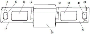
Fig. 1 is a schematic perspective view of a high current-carrying modular photovoltaic module bypass element according to an embodiment of the present invention;
FIG. 2 is a schematic plan view of the modular photovoltaic module bypass element of FIG. 1;
fig. 3 is a schematic plan view of the modular photovoltaic module bypass element of fig. 1 (with the insulating plastic block removed).
Element names and reference symbols in the drawings: 10-first conductive terminal, 11-first bus bar land, 12-first bus bar slot, 20-insulating plastic package block, 22-diode chip, 24-conductive sheet, 30-second conductive terminal, 31-second bus bar land, 32-second bus bar slot, 40-rib.
Detailed Description
In order to further understand the objects, structures, features and functions of the present invention, the following embodiments are described in detail.
Please refer to fig. 1 and fig. 2, which are schematic structural diagrams of a high current-carrying modular photovoltaic module bypass component according to the present invention, the modular photovoltaic module bypass component includes a first conductive terminal 10, an insulating plastic package block 20 and a second conductive terminal 30, the first conductive terminal 10 is provided with a first bus bar welding area 11 and a first bus bar slot 12, and the second conductive terminal 30 is provided with a second bus bar welding area 31 and a second bus bar slot 32; referring to fig. 3, one end of the first conductive terminal 10 adjacent to the second conductive terminal is provided with a bypass protection device first welding region 108 having a rectangular structure, at least one bypass protection device 22 is welded on the bypass protection device first welding region, and the bypass protection device 22 is electrically connected to the second welding region 308 of the second conductive terminal through a conductive sheet 24; the bypass protection device 22 and the conducting strip 24 are packaged in the insulating plastic package block 20 and integrated with the first conducting terminal 10 and the second conducting terminal 30; the edges 212, 232 of the insulating plastic block 20 to which the first and second conductive terminals are secured are tangent to the inner edges 122, 332 of the first and second bus-bar slotted holes 12, 32, respectively.
In a preferred embodiment, in order to adapt to the application of large current, the area of the plane part of the conductive terminal is maximized, as shown in fig. 3, a plurality of bypass protection elements 22 are uniformly spaced on the first welding area 108 of the first conductive terminal 10, so that the capability of passing large current of the high-power photovoltaic module can be adapted, and the current spreading capability of the bypass element of the modular photovoltaic module can be improved by the large-area copper plate plane of the conductive terminal.
In another preferred embodiment, the first conductive terminal 10 and the second conductive terminal 30 are respectively provided with at least one positioning structure 14 and 34, so that the modular photovoltaic module bypass element can be quickly and accurately positioned in the box body when the junction box is produced; in a preferred embodiment, the positioning structure 13 of one of the conductive terminals, for example, the first conductive terminal 10, is a circular hole, and the positioning structure 34 of the other conductive terminal, for example, the second conductive terminal 30, is a rectangular slot, and a protrusion with a corresponding shape is disposed in the assembly junction box, so that the assembly junction box can achieve a foolproof effect during installation, and prevent the module from being installed reversely.
In another preferred embodiment, the first welding area 108 and the second welding area 308 are provided with surface embossing structure, so that solder flowing during welding can be avoided, and the welding effect is more reliable.
In another preferred embodiment, in order to ensure the convenience and reliability of welding the bus bar and the conductive terminals of the assembly, the first bus bar welding area 11 and the second bus bar welding area 31 are recessed structures, which may be recessed structures formed by directly stamping on the conductive terminals, so that a certain amount of solder may be pre-stored in the welding areas 11, 31 before the bus bar is welded, and thus, the efficiency of welding the bus bar may be improved.
In another preferred embodiment, when the modular photovoltaic module bypass element is welded with the cable, the cable is directly connected and fixed with the end part of the first conductive terminal and/or the second conductive terminal in a resistance welding manner; preferably, in order to enhance the effect of the resistance welding, the end parts of the first conductive terminal and the second conductive terminal are provided with convex ribs 40, and the convex ribs are raised structures with certain height formed by directly stamping materials with certain width and length at the end parts of the conductive terminals by adopting a stamping process. In practical application, in order to meet different application requirements, the protruding rib 40 may be disposed at an end of any one of the first conductive terminal and the second conductive terminal, or disposed at both ends of the first conductive terminal and the second conductive terminal, which is not limited by the present invention.
It should be understood that, in the present invention, the conductive terminal on the left side in the bypass element of the modular photovoltaic module in the drawings is referred to as the first conductive terminal, and the conductive terminal on the right side is referred to as the second conductive terminal, which is only for the purpose of clearly describing the embodiments of the present invention, and is not intended to limit the position where the bypass protection element is disposed; in a specific implementation, a user may also set the right conductive terminal as the first conductive terminal and the left conductive terminal as the second conductive terminal in the above embodiment, which should be regarded as an equivalent implementation of the above embodiment.
In addition, it should be understood that the bypass protection device 22 of the present invention may adopt a diode chip as the protection device of the modular bypass element, and may also adopt an integrated circuit module with a bypass protection function as the protection device, which is not particularly limited by the present invention.
The utility model adopts the integrated packaging technology of the conductive terminal and the diode, avoids secondary switching, enhances the conductivity of the diode, simplifies the process and reduces the volume of the modular photovoltaic bypass element; can conveniently set up a plurality of bypass protection devices on conductive terminal, increase the current-carrying capacity of bypass component, design the edge that insulating plastic envelope piece and conductive terminal are fixed simultaneously for tangent with the inboard edge of converging the slotted hole, utilize the restriction of slotted hole ejector pin when can being convenient for the shaping, produce the burr at the edge of insulating plastic envelope piece when avoiding moulding plastics, improve the product yield.
According to another object of the present invention, the present invention also provides a photovoltaic module junction box, which comprises a box body, a box cover and a high current-carrying modular photovoltaic module bypass element arranged in the box body as described above. The junction box can be a single-body junction box used alone or a split junction box used in combination. When being applied to the split type terminal box of the combined use of constituteing by left box body, well box body, right box body, can install the modularization photovoltaic bypass component of isostructure in left box body, well box body, right box body to can adopt a structure to be applied to in different box bodies, satisfy the installation demand, avoid adding the binding post of multiple structure of production man-hour at the terminal box, save extra stamping die's input, and make things convenient for the management of spare part in the production process, save the cost, raise the efficiency.
The present invention has been described in relation to the above embodiments, which are only examples for implementing the present invention. It should be noted that the disclosed embodiments do not limit the scope of the invention. On the contrary, all changes and modifications which do not depart from the spirit and scope of the present invention are deemed to fall within the scope of the present invention.
Claims (9)
1. A high current-carrying modularized photovoltaic assembly bypass element is characterized by comprising a first conductive terminal, an insulating plastic package block and a second conductive terminal, wherein the first conductive terminal is provided with a first converging belt welding area and a first converging belt slot hole, and the second conductive terminal is provided with a second converging belt welding area and a second converging belt slot hole; the first end of the first conductive terminal, which is adjacent to the second conductive terminal, is provided with a first welding area of a bypass protection device with a rectangular structure, at least one bypass protection device is welded on the first welding area, and the bypass protection device is electrically connected with a second welding area of the second conductive terminal through a conducting strip; the bypass protection device and the conducting plate are packaged in the insulating plastic packaging block and integrated with the first conducting terminal and the second conducting terminal into a whole; the edges of the insulating plastic package block, which are fixed with the first conductive terminal and the second conductive terminal, are respectively tangent with the inner side edge of the first converging slotted hole and the inner side edge of the second converging slotted hole.
2. The high current carrying modular photovoltaic module bypass element according to claim 1, wherein a plurality of bypass protection devices are spaced evenly across the first land of the first conductive terminal.
3. The high current carrying modular photovoltaic module bypass element according to claim 1 or 2, wherein the first and second conductive terminals are respectively provided with at least one positioning structure, and the positioning structures on the first and second conductive terminals have different shapes.
4. High current carrying modular photovoltaic module bypass element according to claim 1 or 2, characterized in that the first and second welding areas are provided as surface embossed structures.
5. A high current carrying modular photovoltaic module bypass element as claimed in claim 1 or 2, wherein said first and second bus bar lands are recessed.
6. The high current carrying modular photovoltaic module bypass element according to claim 1 or 2, wherein the modular photovoltaic module bypass element is fixed to the cable by resistance welding, and ribs are provided at the ends of the first and second conductive terminals.
7. The high current carrying modular photovoltaic module bypass element according to claim 1 or 2, wherein the bypass protection device is a diode chip or an integrated circuit module with bypass protection function.
8. A photovoltaic module junction box comprising a box body, a box cover, and a high current carrying modular photovoltaic module bypass element according to any one of claims 1-7 disposed in the box body.
9. The photovoltaic module junction box of claim 8 wherein said junction box is a single piece junction box or a split piece junction box.
Priority Applications (1)
| Application Number | Priority Date | Filing Date | Title |
|---|---|---|---|
| CN202022775349.6U CN213426103U (en) | 2020-11-26 | 2020-11-26 | High current-carrying modularized photovoltaic assembly bypass element and photovoltaic assembly junction box |
Applications Claiming Priority (1)
| Application Number | Priority Date | Filing Date | Title |
|---|---|---|---|
| CN202022775349.6U CN213426103U (en) | 2020-11-26 | 2020-11-26 | High current-carrying modularized photovoltaic assembly bypass element and photovoltaic assembly junction box |
Publications (1)
| Publication Number | Publication Date |
|---|---|
| CN213426103U true CN213426103U (en) | 2021-06-11 |
Family
ID=76251933
Family Applications (1)
| Application Number | Title | Priority Date | Filing Date |
|---|---|---|---|
| CN202022775349.6U Active CN213426103U (en) | 2020-11-26 | 2020-11-26 | High current-carrying modularized photovoltaic assembly bypass element and photovoltaic assembly junction box |
Country Status (1)
| Country | Link |
|---|---|
| CN (1) | CN213426103U (en) |
Cited By (1)
| Publication number | Priority date | Publication date | Assignee | Title |
|---|---|---|---|---|
| CN114498123A (en) * | 2022-02-18 | 2022-05-13 | 中山得意电子有限公司 | Electrical connector |
-
2020
- 2020-11-26 CN CN202022775349.6U patent/CN213426103U/en active Active
Cited By (1)
| Publication number | Priority date | Publication date | Assignee | Title |
|---|---|---|---|---|
| CN114498123A (en) * | 2022-02-18 | 2022-05-13 | 中山得意电子有限公司 | Electrical connector |
Similar Documents
| Publication | Publication Date | Title |
|---|---|---|
| CN216288418U (en) | Improved shaft type diode, bypass module using same and photovoltaic module junction box | |
| CN111769798A (en) | An improved modular photovoltaic module bypass element and module junction box | |
| CN213071116U (en) | Improved modular photovoltaic module bypass element and module junction box | |
| CN211791434U (en) | Large-current photovoltaic junction box structure | |
| CN111969947A (en) | Photovoltaic module bypass element assembly with excellent heat dissipation performance and junction box | |
| CN111245362A (en) | Modular photovoltaic bypass element with turn-ups heat radiation structure | |
| CN112994611A (en) | Low-cost large-current split type photovoltaic module junction box | |
| CN111834320A (en) | Improved Modular PV Module Bypass Element and Module Junction Box | |
| CN212783439U (en) | High current-carrying modularized photovoltaic assembly bypass element and junction box | |
| CN212305259U (en) | Improved modularized photovoltaic assembly bypass element and assembly junction box | |
| CN212572474U (en) | Novel modularized photovoltaic assembly bypass element and junction box | |
| CN212572473U (en) | Modular photovoltaic bypass element | |
| CN212278193U (en) | Improved modular photovoltaic module bypass element and module junction box | |
| CN213072572U (en) | Photovoltaic module bypass element assembly with excellent heat dissipation performance and junction box | |
| CN214412668U (en) | Improved split type photovoltaic assembly junction box | |
| CN112701102B (en) | Photovoltaic module bypass element module and split photovoltaic module junction box having the same | |
| CN218570187U (en) | Low-cost heavy current photovoltaic module terminal box | |
| CN218162390U (en) | Low-cost photovoltaic module terminal box | |
| CN213212157U (en) | Photovoltaic module bypass element soldering lug, bypass protection element module and junction box | |
| CN214591313U (en) | Low-cost split type photovoltaic module junction box adopting axial diodes | |
| CN113783525A (en) | Novel modularized photovoltaic assembly bypass element and junction box | |
| CN212278186U (en) | Low-cost modularization photovoltaic module bypass component and have its terminal box | |
| CN211429265U (en) | Modular photovoltaic bypass element with turn-ups heat radiation structure | |
| CN214900790U (en) | Split type terminal box of solar photovoltaic module | |
| CN215934812U (en) | Bypass module for high-current junction box with good heat dissipation performance and junction box with bypass module |
Legal Events
| Date | Code | Title | Description |
|---|---|---|---|
| GR01 | Patent grant | ||
| GR01 | Patent grant |