CN209948727U - Charging circuit - Google Patents
Charging circuit Download PDFInfo
- Publication number
- CN209948727U CN209948727U CN201920819781.5U CN201920819781U CN209948727U CN 209948727 U CN209948727 U CN 209948727U CN 201920819781 U CN201920819781 U CN 201920819781U CN 209948727 U CN209948727 U CN 209948727U
- Authority
- CN
- China
- Prior art keywords
- circuit
- charging
- chip
- mcu module
- output
- Prior art date
- Legal status (The legal status is an assumption and is not a legal conclusion. Google has not performed a legal analysis and makes no representation as to the accuracy of the status listed.)
- Expired - Fee Related
Links
Images


Landscapes
- Charge And Discharge Circuits For Batteries Or The Like (AREA)
Abstract
本实用新型属于充电技术领域,且公开了一种充电电路,包括充电端口电路;控制电路,所述控制电路包括第一MCU模块、第一开关电路;所述第一MCU模块连接与充电端口电路连接,且所述第一MCU模块,从充电端口电路得到外部充电设备的连接信号,经处理后通过第一开关电路输出给下级电路。
The utility model belongs to the technical field of charging, and discloses a charging circuit, comprising a charging port circuit; a control circuit, wherein the control circuit comprises a first MCU module and a first switch circuit; the first MCU module is connected to a charging port circuit connection, and the first MCU module obtains the connection signal of the external charging device from the charging port circuit, and outputs it to the lower-level circuit through the first switch circuit after processing.
Description
技术领域technical field
本实用新型属于充电技术领域,具体涉及一种充电电路。The utility model belongs to the technical field of charging, in particular to a charging circuit.
背景技术Background technique
目随着市场上智能手机的普及,以及智能手机待机时间短的特点,针对手机的充电设备也日益的增多,同时智能手机的品牌的类型也同时增多,另外各品牌对无线充电技术,有的品牌手机设定了充电协议,因此在不符合充电协议的情况下,很难对手机进行充电;这样就阻碍了无线充电领域的发展,另外无线充电充电速度慢也是行业的通病,因此改变充电的速度也是必要的。With the popularity of smart phones in the market and the short standby time of smart phones, the number of charging devices for mobile phones is also increasing, and the types of smart phone brands are also increasing. The brand mobile phone has set a charging protocol, so it is difficult to charge the mobile phone if it does not meet the charging protocol; this hinders the development of the wireless charging field, and the slow charging speed of wireless charging is also a common problem in the industry, so changing the charging method Speed is also necessary.
实用新型内容Utility model content
本实用新型的目的在于提供一种充电电路,以解决上述背景技术中提出的品牌手机设定了充电协议、无线充电充电速度慢的问题。The purpose of the present invention is to provide a charging circuit to solve the problem of slow charging speed of wireless charging due to the charging protocol set for the brand mobile phone proposed in the above-mentioned background art.
为实现上述目的,本实用新型提供如下技术方案:一种充电电路,包括,In order to achieve the above purpose, the utility model provides the following technical solutions: a charging circuit, comprising,
充电端口电路;charging port circuit;
控制电路,所述控制电路包括第一MCU模块、第一开关电路;所述第一MCU模块连接与充电端口电路连接,且所述第一MCU模块,从充电端口电路得到外部充电设备的连接信号,经处理后通过第一开关电路输出给下级电路;a control circuit, the control circuit includes a first MCU module and a first switch circuit; the first MCU module is connected to a charging port circuit, and the first MCU module obtains a connection signal of an external charging device from the charging port circuit , after processing, it is output to the lower circuit through the first switch circuit;
电源管理电路;所述电源管理电路包括是电源、升压电路、第二MCU模块、第二开关电路;所述升压电路的一输入端与电源连接,所述升压电路的输出端、第一开关电路输出与第二MCU模块的对应输入端连接,所述第二MCU模块的输出经第二开关电路与充电端口电路及下级电路连接;a power management circuit; the power management circuit includes a power supply, a booster circuit, a second MCU module, and a second switch circuit; an input end of the booster circuit is connected to a power supply, and an output end of the booster circuit, a second switch circuit The output of a switch circuit is connected to the corresponding input terminal of the second MCU module, and the output of the second MCU module is connected to the charging port circuit and the lower-level circuit through the second switch circuit;
无线充电路,所述无线充电路的输入端与第二开关电路的输入端连接,所述无线充电路的输出端连接发送线圈。A wireless charging circuit, the input end of the wireless charging circuit is connected with the input end of the second switch circuit, and the output end of the wireless charging circuit is connected with the sending coil.
优选的,所述第一MCU模块包括ES7P003芯片及其外围电路;所述ES7P003芯片对应的输入端与充电端口电路电性连接,所述ES7P003芯片的对应输出端与第一开关电路、第二MCU模块的对应端口电性连接。Preferably, the first MCU module includes an ES7P003 chip and its peripheral circuits; the corresponding input end of the ES7P003 chip is electrically connected to the charging port circuit, and the corresponding output end of the ES7P003 chip is connected to the first switch circuit and the second MCU. The corresponding ports of the modules are electrically connected.
优选的,所述第一开关电路设为SGM3002芯片及其外围电路;所述SGM3002芯片对应的输入端与ES7P003芯片对应的输出端电性连接,所述SGM3002芯片对应的输出端与第二MCU模块对应端电性连接。Preferably, the first switch circuit is set as the SGM3002 chip and its peripheral circuits; the input terminal corresponding to the SGM3002 chip is electrically connected to the output terminal corresponding to the ES7P003 chip, and the output terminal corresponding to the SGM3002 chip is connected to the second MCU module. The corresponding terminals are electrically connected.
优选的,所述升压电路包括第一升压电路、第二升压电路;所述第一升压电路设一储能电感,所述第二升压电路包括多个储能电容构成的电路;所述第一升压电路连分别连接电源及第二MCU模块对应的输入端,所述第二升压电路连接第二MCU模块对应的输出端。Preferably, the booster circuit includes a first booster circuit and a second booster circuit; the first booster circuit is provided with an energy storage inductor, and the second booster circuit includes a circuit composed of a plurality of energy storage capacitors ; The first boost circuit is connected to the power supply and the corresponding input terminals of the second MCU module, respectively, and the second boost circuit is connected to the corresponding output terminal of the second MCU module.
优选的,所述第二MCU模块包括QFN40芯片及其外围电路;所述QFN40芯片的对应输入端与储能电感、SGM3002芯片对应的输出端电性连接;所述QFN40芯片对应输出端经多个储能电容的公共端,分别与充电端口电路、无线充电路电性连接。Preferably, the second MCU module includes a QFN40 chip and its peripheral circuits; the corresponding input end of the QFN40 chip is electrically connected to the energy storage inductor and the output end corresponding to the SGM3002 chip; the corresponding output end of the QFN40 chip is connected through a plurality of The common terminal of the energy storage capacitor is electrically connected to the charging port circuit and the wireless charging circuit respectively.
优选的,所述第二开关电路包括多个SOT23-6芯片及其外围电路;所述SOT23-6芯片的一输入端均通过多个储能电容的公共端与QFN40芯片对应的输出端电性连接,所述多个SOT23-6芯片的输出端对应与充电端口电路、无线充电路电性连接。Preferably, the second switch circuit includes a plurality of SOT23-6 chips and their peripheral circuits; an input end of the SOT23-6 chip is electrically connected to an output end corresponding to the QFN40 chip through the common end of the plurality of energy storage capacitors connected, the output ends of the plurality of SOT23-6 chips are correspondingly electrically connected with the charging port circuit and the wireless charging circuit.
优选的,所述无线充电路包括放无线发射电路、主控电路、协议诱骗电路;所述无线发射电路的对应输入端与其中一SOT23-6芯片的输出端、主控电路对应的输出端电性连接;所述主控电路的对应输入端与协议诱骗电路的输出端连接;所述协议诱骗电路的输入端与充电端口电路电性连接。Preferably, the wireless charging circuit includes a wireless transmitting circuit, a main control circuit, and a protocol decoy circuit; the corresponding input end of the wireless transmitting circuit is electrically connected to the output end of one of the SOT23-6 chips and the output end corresponding to the main control circuit. The corresponding input end of the main control circuit is connected with the output end of the protocol decoy circuit; the input end of the protocol decoy circuit is electrically connected with the charging port circuit.
优选的,所述主控电路设为一MCU芯片及其外围电路,所述协议诱骗电路设多个电阻构成的电路。Preferably, the main control circuit is set as an MCU chip and its peripheral circuits, and the protocol decoy circuit is set as a circuit composed of a plurality of resistors.
所述充电端口电路连接外部的被充电单元或电源;且所述充电端口电路连接外部被充电单元或电源后,将信号反溃经第一开关电路传送给第一MCU模块的对应输入端,第一MCU模块的输出端经下级电路处理后进行放电或充电。The charging port circuit is connected to an external charged unit or power source; and after the charging port circuit is connected to an external charged unit or power source, the signal is transmitted to the corresponding input end of the first MCU module through the first switch circuit, and the first The output end of an MCU module is discharged or charged after being processed by the subordinate circuit.
与现有技术相比,本实用新型的有益效果是:Compared with the prior art, the beneficial effects of the present utility model are:
(1)本实用新型“协议诱骗电路”通过充电端口电路、第二开关电路、QFN40芯片,从电源诱骗QC的5V或9V;然后再经主控电路输送给到“发射电路”;“发射电路”将输入的直流5V或9V逆变转换成高频交流电,从而在线圈上产生磁场,然后通过电磁感应原理,将能量传递给外部充电设备(手机);这样的设计方式在不符合苹果手机充电协议的条件下,可以进行对苹果手机的无线充电,另外也方便安卓手机的无线充电。(1) The "protocol decoy circuit" of the present utility model deceives 5V or 9V of the QC from the power supply through the charging port circuit, the second switch circuit and the QFN40 chip; "Convert the input DC 5V or 9V into high-frequency alternating current, so as to generate a magnetic field on the coil, and then transfer the energy to the external charging device (mobile phone) through the principle of electromagnetic induction; this design method is not in line with Apple mobile phone charging. Under the conditions of the agreement, wireless charging of Apple mobile phones can be carried out, and it is also convenient for wireless charging of Android mobile phones.
(2)本实用新型电源(电池)通过升压电路、QFN40芯片、第二开关电路、充电端品电路进行对外部的充电单元(手机)进行充电,或者是通过充电端品电路、第二开关电路、QFN40芯、片升压电路对电源进行充,这样的设计方式方便外部的充电单元(手机)充电,也可以方便在电源(电池)电量不足时,通过充电端口电路对电源(电池)进行充电;因此本实用新型专利具有多功能充电方式、充电方便、充电速度快的有益效果。(2) The power supply (battery) of the utility model charges the external charging unit (mobile phone) through the booster circuit, the QFN40 chip, the second switch circuit and the charging terminal circuit, or through the charging terminal circuit, the second switch The circuit, QFN40 chip, and chip boost circuit are used to charge the power supply. This design method is convenient for charging the external charging unit (mobile phone), and it is also convenient for the power supply (battery) to be charged through the charging port circuit when the power supply (battery) is insufficient. Therefore, the utility model patent has the beneficial effects of multifunctional charging mode, convenient charging and fast charging speed.
附图说明Description of drawings
图1为本实用新型的充电端口电路原理图;1 is a schematic diagram of a charging port circuit of the present invention;
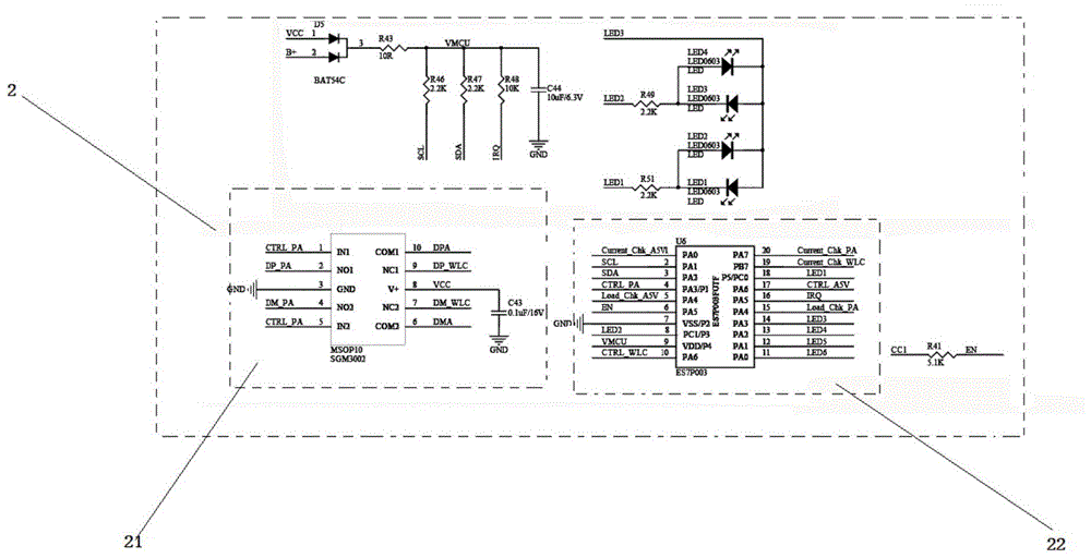
图2为本实用新型的控制电路原理图;Fig. 2 is the control circuit principle diagram of the utility model;
图3为本实用新型的电源管理电路原理图;3 is a schematic diagram of a power management circuit of the present invention;
图4为本实用新型的无线充电路原理图。FIG. 4 is a schematic diagram of a wireless charging circuit of the present invention.
具体实施方式Detailed ways
下面将结合本实用新型实施例中的附图,对本实用新型实施例中的技术方案进行清楚、完整地描述,显然,所描述的实施例仅仅是本实用新型一部分实施例,而不是全部的实施例。基于本实用新型中的实施例,本领域普通技术人员在没有做出创造性劳动前提下所获得的所有其他实施例,都属于本实用新型保护的范围。The technical solutions in the embodiments of the present utility model will be clearly and completely described below with reference to the accompanying drawings in the embodiments of the present utility model. Obviously, the described embodiments are only a part of the embodiments of the present utility model, rather than all the implementations. example. Based on the embodiments of the present invention, all other embodiments obtained by those of ordinary skill in the art without creative work fall within the protection scope of the present invention.
请参阅图1-图4所示,本实用新型提供一种技术方案:一种充电电路,包括;Please refer to FIG. 1-FIG. 4, the present utility model provides a technical solution: a charging circuit, comprising;
充电端口电路3;
控制电路2,所述控制电路2包括第一MCU模块22、第一开关电路21;所述第一MCU模块22连接与充电端口电路3连接,且所述第一MCU模块22,从充电端口电路3得到外部充电设备的连接信号,经处理后通过第一开关电路21输出给下级电路;
电源管理电路1;所述电源管理电路1包括是电源11、升压电路、第二MCU模块15、第二开关电路14;所述升压电路的一输入端与电源11连接,所述升压电路的输出端、第一开关电路21输出与第二MCU模块15的对应输入端连接,所述第二MCU模块15的输出经第二开关电路14与充电端口电路3及下级电路连接;A
无线充电路4,所述无线充电路4的输入端与第二开关电路14的输入端连接,所述无线充电路4的输出端连接发送线圈。The
所述第一MCU模块22包括ES7P003芯片及其外围电路;所述ES7P003芯片对应的输入端与充电端口电路3电性连接,所述ES7P003芯片的对应输出端与第一开关电路21、第二MCU模块15的对应端口电性连接;所述ES7P003芯片的外围电路设为4个LED灯和多个电组构成的电路,其4个LED灯用来显示电源11(电池)的电量。The
所述第一开关电路21设为SGM3002芯片及其外围电路;所述SGM3002芯片对应的输入端与ES7P003芯片对应的输出端电性连接,所述SGM3002芯片对应的输出端与第二MCU模块15对应端电性连接。The
所述升压电路包括第一升压电路12、第二升压电路13;所述第一升压电路12设一储能电感,所述第二升压电路13包括多个储能电容构成的电路;所述第一升压电路12连分别连接电源11及第二MCU模块15对应的输入端,所述第二升压电路13连接第二MCU模块15对应的输出端。The booster circuit includes a
所述第二MCU模块15包括QFN40芯片及其外围电路;所述QFN40芯片的对应输入端与储能电感、SGM3002芯片对应的输出端电性连接;所述QFN40芯片对应输出端经多个储能电容的公共端,分别与充电端口电路3、无线充电路4电性连接。The
所述第二开关电路14包括多个SOT23-6芯片及其外围电路;所述SOT23-6芯片的一输入端均通过多个储能电容的公共端与QFN40芯片对应的输出端电性连接,所述多个SOT23-6芯片的输出端对应与充电端口电路3、无线充电路4电性连接。The
所述无线充电路4包括放无线发射电路41、主控电路43、协议诱骗电路43;所述无线发射电路41的对应输入端与其中一SOT23-6芯片的输出端、主控电路43对应的输出端电性连接;所述主控电路43的对应输入端与协议诱骗电路43的输出端连接;所述协议诱骗电路43的输入端与充电端口电路3电性连接。The
所述主控电路43设为一MCU芯片及其外围电路,所述协议诱骗电路43设多个电阻构成的电路。The main control circuit 43 is set as an MCU chip and its peripheral circuits, and the protocol decoy circuit 43 is set as a circuit composed of a plurality of resistors.
所述充电端口电路3连接外部的被充电单元或电源11;且所述充电端口电路3连接外部被充电单元或电源11后,将信号反溃经第一开关电路21传送给第一MCU模块22的对应输入端,第一MCU模块22的输出端经下级电路处理后进行放电或充电。The
实施例:Example:
一种充电电路还包括电源11(电池)保护电路,晶振电路、调制电路;所述电源11(电池)保护电路用来保电源11的过充,过放,过压,欠压等状态,从而有效保护电源11(电池),所述晶振电路、调制电路均与无线充电路44电性连接。A charging circuit also includes a power supply 11 (battery) protection circuit, a crystal oscillator circuit, and a modulation circuit; the power supply 11 (battery) protection circuit is used to protect the
本实用新型的工作原理:The working principle of the present utility model:
(1)、首先协议诱骗电路43”通过充电端口电路3、第二开关电路14、QFN40芯片,从电源11诱骗QC的5V或9V;然后再经主控电路43输送给到“发射电路”;“发射电路”将输入的直流5V或9V逆变转换成高频交流电,从而在线圈上产生磁场,然后通过电磁感应原理,将能量传递给外部充电设备(手机);其中“晶振电路”可以提供一个固定频率,以满足不同外部充电设备所需功率;“调制电路”可检测线圈是否有金属异物,是否过流等,“主控电路43”控制无线充不同状态的亮灯方式,以及对过温.过流.异物等状态做出响应;(1) First, the protocol decoy circuit 43" deceives 5V or 9V of QC from the
(2)、放电的时候:由电源11(电池)给“电源11管理”部分供电,该部分内部集成了BOOST升压电路,以及快充协议识别芯片,将电芯电压由4.2V升压到5V/9V/12V,然后通过“接口部分”输出到外部充电设备。(2) When discharging: the power supply 11 (battery) supplies power to the "
(3)、充电的时候:当外部电源11给本产品充电时,外部电源11供5V/9V/12V给充电端口,然后给到电源11管理部分,电源11管理部分集成了高效率的开关充电,将输入电压降为4.2V给电池充电。“电池保护电路”该电路可以检测电源11(电池)过充,过放,过压,欠压等状态,从而有效保护电池。(3) When charging: When the
尽管已经示出和描述了本实用新型的实施例,对于本领域的普通技术人员而言,可以理解在不脱离本实用新型的原理和精神的情况下可以对这些实施例进行多种变化、修改、替换和变型,本实用新型的范围由所附权利要求及其等同物限定。Although the embodiments of the present invention have been shown and described, it will be understood by those skilled in the art that various changes and modifications can be made to these embodiments without departing from the principles and spirit of the present invention , alternatives and modifications, the scope of the present invention is defined by the appended claims and their equivalents.
Claims (8)
Priority Applications (1)
| Application Number | Priority Date | Filing Date | Title |
|---|---|---|---|
| CN201920819781.5U CN209948727U (en) | 2019-05-30 | 2019-05-30 | Charging circuit |
Applications Claiming Priority (1)
| Application Number | Priority Date | Filing Date | Title |
|---|---|---|---|
| CN201920819781.5U CN209948727U (en) | 2019-05-30 | 2019-05-30 | Charging circuit |
Publications (1)
| Publication Number | Publication Date |
|---|---|
| CN209948727U true CN209948727U (en) | 2020-01-14 |
Family
ID=69135010
Family Applications (1)
| Application Number | Title | Priority Date | Filing Date |
|---|---|---|---|
| CN201920819781.5U Expired - Fee Related CN209948727U (en) | 2019-05-30 | 2019-05-30 | Charging circuit |
Country Status (1)
| Country | Link |
|---|---|
| CN (1) | CN209948727U (en) |
Cited By (1)
| Publication number | Priority date | Publication date | Assignee | Title |
|---|---|---|---|---|
| CN111722141A (en) * | 2020-06-30 | 2020-09-29 | 深圳市华美兴泰科技股份有限公司 | A programmable charging and discharging tester with fast charging protocol |
-
2019
- 2019-05-30 CN CN201920819781.5U patent/CN209948727U/en not_active Expired - Fee Related
Cited By (1)
| Publication number | Priority date | Publication date | Assignee | Title |
|---|---|---|---|---|
| CN111722141A (en) * | 2020-06-30 | 2020-09-29 | 深圳市华美兴泰科技股份有限公司 | A programmable charging and discharging tester with fast charging protocol |
Similar Documents
| Publication | Publication Date | Title |
|---|---|---|
| CN103208850B (en) | The USB charging system of charge-variable voltage, charger and intelligent terminal | |
| CN105576727B (en) | Method, device and system for quick charging | |
| CN103107584A (en) | Device with wireless mobile charging function and wireless charging method thereof | |
| CN116742740A (en) | A charging device and electronic equipment | |
| CN104917267A (en) | Two-in-one charging circuit compatible with MTK and QC2.0 charging schemes | |
| CN204992701U (en) | Quick charging device of portable power source | |
| CN102769323A (en) | Ultra-fast charge equipment for mobile phone batteries | |
| CN214154112U (en) | Two-in-one power supply | |
| CN204928297U (en) | Mobile power supply | |
| CN205407320U (en) | a charger | |
| CN204761142U (en) | Compatible MTK and QC2. 0 charging scheme's two unification charging circuit | |
| CN204441950U (en) | Charging device and electronic equipment that can be adapted to different electronic equipment | |
| CN106300466A (en) | Method, device and the terminal of a kind of OTG quick charge | |
| CN206293924U (en) | mobile power | |
| CN214380174U (en) | a mobile power | |
| CN110289663A (en) | A terminal device and its power circuit and power adapter | |
| CN206077020U (en) | A kind of non-contact charger systems | |
| CN116111693A (en) | Charging control circuit and method of active capacitive pen and active capacitive pen | |
| CN210577830U (en) | Notebook with function of charging | |
| CN206850536U (en) | A kind of simple and practical radio energy-transmitting charger | |
| CN207677747U (en) | An ethernet power conversion system | |
| CN207200312U (en) | A kind of quick-charging circuit and portable power source | |
| CN221176596U (en) | Battery device and electronic equipment | |
| CN223079775U (en) | Mobile power supply control circuit with quick charging function and mobile power supply | |
| CN206211606U (en) | a fast charger |
Legal Events
| Date | Code | Title | Description |
|---|---|---|---|
| GR01 | Patent grant | ||
| GR01 | Patent grant | ||
| CF01 | Termination of patent right due to non-payment of annual fee | ||
| CF01 | Termination of patent right due to non-payment of annual fee |
Granted publication date: 20200114 |