CN201450324U - A surge absorber - Google Patents
A surge absorber Download PDFInfo
- Publication number
- CN201450324U CN201450324U CN2009200038408U CN200920003840U CN201450324U CN 201450324 U CN201450324 U CN 201450324U CN 2009200038408 U CN2009200038408 U CN 2009200038408U CN 200920003840 U CN200920003840 U CN 200920003840U CN 201450324 U CN201450324 U CN 201450324U
- Authority
- CN
- China
- Prior art keywords
- diode
- pin
- surge absorber
- doped region
- surge
- Prior art date
- Legal status (The legal status is an assumption and is not a legal conclusion. Google has not performed a legal analysis and makes no representation as to the accuracy of the status listed.)
- Expired - Fee Related
Links
Images


Landscapes
- Emergency Protection Circuit Devices (AREA)
Abstract
本实用新型是关于一种突波吸收器,其包含一第一二极管、一第二二极管与一第三接脚,第一二极管具有一第一接脚,第二二极管连接于第一二极管,且具有一第二接接脚,第三接脚设置于第一二极管与第二二极管的接合处。本实用新型将第三接脚耦接于第一二极管与第二二极管接合处,其可有效引出突波能量,而有效降低突波吸收器本身的温度,进而提升突波吸收器的可靠度。
The utility model relates to a surge absorber, which includes a first diode, a second diode and a third pin. The first diode has a first pin, the second diode is connected to the first diode and has a second pin, and the third pin is arranged at the junction of the first diode and the second diode. The utility model couples the third pin to the junction of the first diode and the second diode, which can effectively lead out surge energy and effectively reduce the temperature of the surge absorber itself, thereby improving the reliability of the surge absorber.
Description
技术领域technical field
本实用新型是关于一种吸收器,特别是指一种突波吸收器。The utility model relates to an absorber, in particular to a surge absorber.
背景技术Background technique
突波吸收器为一种电路保护组件,主要功能为保护电子电路免于遭受突波的干扰与破坏,应用范围包括信息、通讯及消费性电子产品。一般来说产生突波的主要原因有两种:一种是打雷闪电所产生的雷突波,而另一种是由电路开闭所造成的开闭突波。雷突波是自然界所产生的,因此如果要设计电路,必须在容易产生打雷的地区使用,所以加入适当的保护是有必要的;而开闭突波是电路导通的瞬间所产生的突波,当突波产生时,若电子电路如果没有突波保护,那么电路就容易因开闭突波而产生误动作,甚至可能会导致电路因过载而损坏,或因为长时间受到突波的干扰而使电子产品寿命降低。The surge absorber is a circuit protection component whose main function is to protect electronic circuits from interference and damage caused by surges. Its applications include information, communication and consumer electronics products. Generally speaking, there are two main reasons for the surge: one is the thunder surge generated by thunder and lightning, and the other is the switching surge caused by the circuit switching. Lightning surges are produced by nature, so if you want to design a circuit, you must use it in an area that is prone to lightning, so it is necessary to add appropriate protection; and the switching surge is the surge generated at the moment the circuit is turned on , when the surge occurs, if the electronic circuit does not have surge protection, then the circuit is prone to misoperation due to the switching surge, and may even cause the circuit to be damaged due to overload, or to be damaged due to the interference of the surge for a long time. Reduce the life of electronic products.
请参阅图1,其为运用现有突波吸收器的电源供应器的电路图。如图所示,电源供应器包含一变压器T,其具有一一次侧绕组NP与一二次侧绕组NS,一次侧绕组NP的一端耦接一输入端VCC,以接收输入电源,一次侧绕组NP的另一端耦接一开关Q,开关Q透过一电阻R耦接于接地端。变压器T的二次侧绕组NS的一端耦接一整流器D的一端,一电容C耦接于整流器D的另一端与二次侧绕组NS的另一端之间,电容C0亦耦接于电源供应器的输出端,电源供应器的输出端用于提供一输出电压V0。控制器1依据电阻R所产生的一感测讯号而产生一控制讯号,以控制开关Q的导通与关闭,进而控制变压器T,以调整输出电压V0。输入端VCC更耦接控制器1以提供电源至控制器1。Please refer to FIG. 1 , which is a circuit diagram of a power supply using a conventional surge absorber. As shown in the figure, the power supply includes a transformer T, which has a primary winding N P and a secondary winding N S , and one end of the primary winding N P is coupled to an input terminal V CC for receiving input power. , the other end of the primary winding NP is coupled to a switch Q, and the switch Q is coupled to the ground terminal through a resistor R. One end of the secondary winding NS of the transformer T is coupled to one end of a rectifier D, a capacitor C is coupled between the other end of the rectifier D and the other end of the secondary winding NS , and the capacitor C0 is also coupled to The output end of the power supply, the output end of the power supply is used to provide an output voltage V 0 . The controller 1 generates a control signal according to a sensing signal generated by the resistor R to control the switch Q to be turned on and off, and then controls the transformer T to adjust the output voltage V 0 . The input terminal V CC is further coupled to the controller 1 to provide power to the controller 1 .
由于开关Q会时常切换,如此即会在开关Q的汲极产生高压突波,当此电压突波发生时,若无适当方式抑制则开关Q将会受到过高的电压突波而损坏开关Q,又或者突波的能量影响开关Q的正常频率响应效能,而造成功率损失加大,因而使得开关Q的温度提升,则开关Q的可靠度下降,导致整体电路运作的功率因素恶化。基于上述因素,一突波吸收器5耦接于输入端VCC与开关Q的汲极,以用于消除开关Q所产生的突波。Since the switch Q will switch frequently, a high-voltage surge will be generated at the drain of the switch Q. When the voltage surge occurs, if there is no proper way to suppress the switch Q, the switch Q will be damaged by the excessive voltage surge. , or the energy of the surge affects the normal frequency response performance of the switch Q, resulting in increased power loss, thus increasing the temperature of the switch Q, reducing the reliability of the switch Q, and deteriorating the power factor of the overall circuit operation. Based on the above factors, a
突波吸收器5用于将突波导引至电源端,以消除突波。然而,由于突波所有产生的能量全部经由突波吸收器5导引至电源端,又因突波吸收器5具有一定内阻,所以流经突波吸收器5的较大的电流会转换成较高的温度,如此会造成较高的功率损失,使得有效的功率下降,也因为突波吸收器5本体的温度上升而会致使突波吸收器5的可靠度下降。现今,电子产品发展相当快速且功能相当广泛,如此功率越来越大且体积越来越小,所以工作频率越来越广,且频率越来越高,因此传统的突波吸收器必须加大功率才足以应付所需,但相对其无效功率损耗会越来越高,如此即不符合现今节能诉求,而切耗费电源。The
因此,本实用新型即在针对上述问题而提出一种突波吸收器,不仅可改善突波吸收器无效功率损耗及本身温度升高的缺点,又可增加消除突波的效能与其可靠度,以解决上述问题。Therefore, the utility model proposes a surge absorber in response to the above problems, which can not only improve the shortcomings of the surge absorber’s ineffective power loss and temperature rise, but also increase the effectiveness and reliability of eliminating surges, so as to Solve the above problems.
发明内容Contents of the invention
本实用新型的目的之一,在于提供一种突波吸收器,其通过由增设一第三接脚而与其它电子组件配合,以有效消除高压突波,以降低突波吸收器本身的温度并增加其可靠度。One of the purposes of the present utility model is to provide a surge absorber, which cooperates with other electronic components by adding a third pin to effectively eliminate high-voltage surges, thereby reducing the temperature of the surge absorber itself and increase its reliability.
本实用新型的目的之二,在于提供一种突波吸收器,其通过由整合第一二极管与第二二极管而为单一电子组件,如此可减小用于电子基板中所占用的体积,以改善电路设计应用以及加工的容易度。The second purpose of the present utility model is to provide a surge absorber, which can be used as a single electronic component by integrating the first diode and the second diode, which can reduce the occupied space used in the electronic substrate. volume to improve the ease of circuit design application and processing.
为实现本实用新型的目的及解决其技术问题是通过以下技术方案来实现的。In order to realize the purpose of the utility model and solve its technical problems, it is realized through the following technical solutions.
本实用新型所述的一种突波吸收器,其包含有:一第一二极管,具有一第一接脚;一第二二极管,连接于该第一二极管,且具有一第二接脚;以及一第三接脚,设置于该第一二极管与该第二二极管的接合处。A surge absorber according to the utility model includes: a first diode with a first pin; a second diode connected to the first diode and with a a second pin; and a third pin disposed at the junction of the first diode and the second diode.
本实用新型的有益效果是:本实用新型通过由于第一二极管与第二二极管的接合处设置第三接脚,其可利于直接导引突波能量,而可降低突波吸收器本身的温度,如此即可提升突波吸收器的可靠度。The beneficial effects of the utility model are: the utility model is provided with a third pin at the junction of the first diode and the second diode, which can be beneficial to directly guide the surge energy, and can reduce the surge absorber. The temperature itself, so that the reliability of the surge absorber can be improved.
附图说明Description of drawings
图1为具有现有突波吸收器的电源供应器的电路图;FIG. 1 is a circuit diagram of a power supply with a conventional surge absorber;
图2为本实用新型突波吸收器运用于电源供应器的一较佳实施例的电路图;Fig. 2 is a circuit diagram of a preferred embodiment of the utility model surge absorber applied to a power supply;
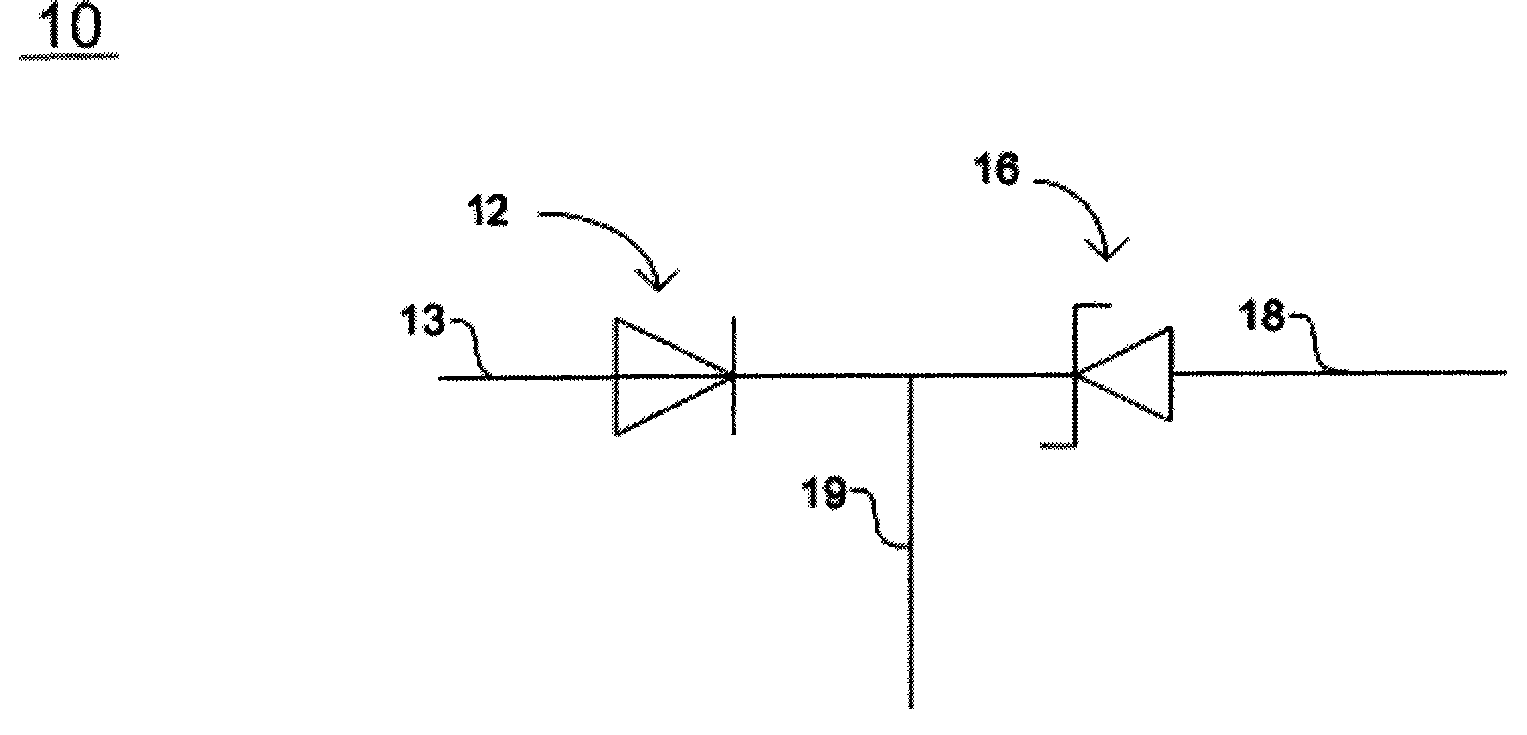
图3为本实用新型突波吸收器的一较佳实施例的电路图;Fig. 3 is the circuit diagram of a preferred embodiment of the utility model surge absorber;
图4为本实用新型突波吸收器的第一较佳实施例的结构图;Fig. 4 is the structural diagram of the first preferred embodiment of the utility model surge absorber;
图5为本实用新型突波吸收器的第二较佳实施例的结构图;Fig. 5 is the structural diagram of the second preferred embodiment of the utility model surge absorber;
图6为本实用新型突波吸收器的第三较佳实施例的结构图;Fig. 6 is the structural view of the third preferred embodiment of the utility model surge absorber;
图7为本实用新型突波吸收器的第四较佳实施例的结构图;Fig. 7 is a structural diagram of a fourth preferred embodiment of the utility model surge absorber;
图8为本实用新型突波吸收器的另一较佳实施例的电路图;Fig. 8 is the circuit diagram of another preferred embodiment of the utility model surge absorber;
图9为本实用新型突波吸收器的第五较佳实施例的结构图;Fig. 9 is a structural diagram of a fifth preferred embodiment of the surge absorber of the present invention;
图10为本实用新型突波吸收器的第六较佳实施例的结构图;Fig. 10 is a structural diagram of a sixth preferred embodiment of the utility model surge absorber;
图11为本实用新型突波吸收器的第七较佳实施例的结构图;以及Fig. 11 is a structural diagram of the seventh preferred embodiment of the utility model surge absorber; and
图12为本实用新型突波吸收器的第八较佳实施例的结构图。Fig. 12 is a structural diagram of the eighth preferred embodiment of the surge absorber of the present invention.
【图号简单说明】[Simple description of figure number]
1 控制器 5 突波吸收器1
10 突波吸收器 12 第一二极管10 surge absorber 12 first diode
121 P极 123 N极121 P pole 123 N pole
125 第一P型掺杂区 126 第一N型掺杂区125 First P-type doped
129 第一N型掺杂区 127 N型井129 first N-type doped region 127 N-type well
128 P型井 13 第一接脚128 P-
16 第二二极管 161 P极16 Second diode 161 P pole
163 N极 165 第二P型掺杂区163
166 第二N型掺杂区 169 第二N型掺杂区166 Second N-type doped
18 第二接脚 19 第三接脚18 The
38 散热层 40 散热层38
C 电容 C1 电容C capacitor C 1 capacitor
C2 电容 CO 电容C 2 capacitance C O capacitance
D 整流器 NP 一次侧绕组D Rectifier N P primary winding
NS 二次侧绕组 Q 开关N S Secondary Winding Q Switch
R 电阻 R2 电阻R resistor R 2 resistor
T 变压器 VO 输出电压T transformer V O output voltage
VCC 输入端V CC input
具体实施方式Detailed ways
为使对本实用新型的结构特征及所达成的功效有更进一步的了解与认识,用以较佳的实施例及配合详细的说明,说明如下:In order to have a further understanding and understanding of the structural features of the present utility model and the achieved effects, for preferred embodiments and detailed descriptions, the descriptions are as follows:
首先,请参阅图2,为本实用新型突波吸收器运用于电源供应器的一较佳实施例的电路图。如图所示,电源供应器包含变压器T,其具有一次侧绕组NP与二次侧绕组NS,一次侧绕组NP耦接输入端VCC以接收输入电源,以在二次侧绕组NS提供输出电压VO。变压器T的二次侧绕组NS耦接整流器D与电容C1,电容C1用于过滤输出电压VO。此外,一次侧绕组NP耦接开关Q,开关Q透过电阻R耦接于接地端控制器1,以依据电阻R所产生的感测讯号而产生控制讯号,以控制开关Q的导通与关闭,进而控制变压器T,以调整输出电压VO。输入端VCC更耦接控制器1以提供电源至控制器1。First, please refer to FIG. 2 , which is a circuit diagram of a preferred embodiment of the surge absorber of the present invention applied to a power supply. As shown in the figure, the power supply includes a transformer T, which has a primary side winding N P and a secondary side winding N S , the primary side winding N P is coupled to the input terminal V CC to receive the input power, and the secondary side winding N S provides the output voltage V O . The secondary winding NS of the transformer T is coupled to the rectifier D and the capacitor C 1 , and the capacitor C 1 is used to filter the output voltage V O . In addition, the primary side winding NP is coupled to the switch Q, and the switch Q is coupled to the ground terminal controller 1 through the resistor R, so as to generate a control signal according to the sensing signal generated by the resistor R, so as to control the conduction and switching of the switch Q. turn off, and then control the transformer T to adjust the output voltage V O . The input terminal V CC is further coupled to the controller 1 to provide power to the controller 1 .
此外,开关Q的汲极与输入端VCC之间耦接本实用新型的突波吸收器10,以用于消除开关Q所产生的高压突波。本实用新型的突波吸收器10具有三只接脚,以通过由第三接脚连接于一电阻R2与一电容C2,而电阻R2与电容C2并耦接于输入端VCC。由于电容C2位于高频状态下时可视为短路,故突波吸收器10可将大部分的突波能量用较低的损耗引导至输入端VCC,如此即可降低发生在突波吸收器10上的损耗,因而可大幅降低突波吸收器10的温度,进而可提高突波吸收器10的可靠度。电容C2的电容值可依据整体电路的需求而调整,所以运用本实用新型的突波吸收器10比现有突波吸收器具有较大的适用范围,亦可提高整体电路的有效功率因素。另外,因本实用新型的突波吸收器10为单一电子组件,且因具有较低的本体温度,所以可作成插件式封装(DIP)型式之外,亦可封装成贴片包装(SMD)型式,而更进一步降低突波吸收器10所占的体积。In addition, the
请参阅图3,为本实用新型突波吸收器的一较佳实施例的电路图。如图所示,本实用新型的突波吸收器10包含一第一二极管12、一第一接脚13、一第二二极管16、一第二接脚18与一第三接脚19。第一接脚13连接于第一二极管12的正极,第二接脚18连接于第二二极管16的正极,而第一二极管12的负极连接于第二二极管16的负极。第三接脚19耦接于第一二极管12与第二二极管16的接合处。第二二极管16的较佳实施例可为一瞬时电压二极管(Transient Voltage Suppressor,TVS),又或者第一二极管12可为瞬时电压二极管。Please refer to FIG. 3 , which is a circuit diagram of a preferred embodiment of the surge absorber of the present invention. As shown in the figure, the
请参阅图4,为本实用新型突波吸收器的第一较佳实施例的结构图.如图所示,本实用新型的突波吸收器10的第一二极管12包含一P极121与一N极123,第二二极管16包含一P极161与一N极163,第一二极管12与第二二极管16的P极121、161即为正极,N极123、163为负极.第一二极管12的N极123与第二二极管16的N极163相连接,即第一二极管12的负极连接于第二二极管16的负极.第一接脚13连接于第一二极管12的P极121,第二接脚18连接于第二二极管16的P极161.第三接脚19设置于第一二极管12的N极123与第二二极管16的N极163的接合处.由于本实用新型的突波吸收器10的第三接脚19设置于第一二极管12与第二二极管16的接合处,且因第一二极管12与第二二极管16产生热能的主要位置为PN极的接面,所以本实用新型突波吸收器10的第三接脚19可有效导引出第一二极管12与第二二极管16所产生的热能,而降低温度,如此突波吸收器10即会因为温度下降,而提高其可靠度.Please refer to Fig. 4, which is a structural diagram of a first preferred embodiment of the surge absorber of the present invention. As shown in the figure, the
请参阅图5,为本实用新型突波吸收器的第二较佳实施例的结构图。如图所示,此实施例与上一实施例的不同之处在于此实施例的突波吸收器10更包含一散热层38,其连接于第一二极管12的N极123与第二二极管16的N极163,而第三接脚19连接于散热层38,如此可通过由散热层38更提高突波吸收器10的散热效果。散热层38可为一散热片。Please refer to FIG. 5 , which is a structural diagram of a second preferred embodiment of the surge absorber of the present invention. As shown in the figure, the difference between this embodiment and the previous embodiment is that the
请参阅图6,为本实用新型突波吸收器的第三较佳实施例的结构图。如图所示,本实用新型的突波吸收器10的第一二极管12与第二二极管16包含一N型井127、一第一P型掺杂区125与一第二P型掺杂区165。第一P型掺杂区125与第二P型掺杂区165位于N型井127且相互间隔。第一接脚13连接于第一P型掺杂区125,第二接脚18连接于第二P型掺杂区165,第三接脚19连接于N型井127。Please refer to FIG. 6 , which is a structural diagram of a third preferred embodiment of the surge absorber of the present invention. As shown in the figure, the
请参阅图7,为本实用新型突波吸收器的第四较佳实施例的结构图。请一并参阅图6,如图所示,此实施例不同于图6实施例之处在于此实施例更具有一散热层40,其设置于N型井127,而第三接脚19连接于散热层40,以利于突波吸收器10散热。Please refer to FIG. 7 , which is a structural diagram of a fourth preferred embodiment of the surge absorber of the present invention. Please also refer to FIG. 6. As shown in the figure, this embodiment is different from the embodiment in FIG. The
请参阅图8,为本实用新型突波吸收器的另一较佳实施例的电路图。请一并参阅图3,如图所示,此实施例不同于图3实施例之处在于此实施例的突波吸收器10的第一二极管12的正极与第二二极管16的正极相连接,且第三接脚19设置于第一二极管12与第二二极管12接合处。Please refer to FIG. 8 , which is a circuit diagram of another preferred embodiment of the surge absorber of the present invention. Please also refer to FIG. 3, as shown in the figure, this embodiment is different from the embodiment of FIG. The anodes are connected, and the
请参阅图9,为本实用新型突波吸收器的第五较佳实施例的结构图。请一并参阅图4,如图所示,此实施例不同于图4实施例之处在于此实施例将第一二极管12的P极121与第二二极管16的P极161相连接,也就是第一二极管12的正极连接第二二极管16的正极。第一接脚13连接于第一二极管12的N极123,第二接脚18连接于第二二极管16的N极163。第三接脚19设置于第一二极管12的P极121与第二二极管16的P极161的接合处。Please refer to FIG. 9 , which is a structural diagram of a fifth preferred embodiment of the surge absorber of the present invention. Please also refer to FIG. 4, as shown in the figure, this embodiment is different from the embodiment in FIG. connection, that is, the anode of the
请参阅图10,为本实用新型突波吸收器的第六较佳实施例的结构图。请一并参阅图5,如图所示,此实施例不同于图5实施例之处在于此实施例第一二极管12的P极121与第二二极管16的P极161连接散热层38。第一接脚13连接于第一二极管12的N极123,第二接脚18连接于第二二极管18的N极163,第三接脚19设连接于散热层38。Please refer to FIG. 10 , which is a structural diagram of a sixth preferred embodiment of the surge absorber of the present invention. Please refer to FIG. 5 together. As shown in the figure, this embodiment is different from the embodiment in FIG. 5 in that the
请参阅图11,为本实用新型突波吸收器的第七较佳实施例的结构图。请一并参阅图6,如图所示,此实施例不同于图6实施例之处在于此实施例的第一二极管12与第二二极管16包含一P型井128、一第一N型掺杂区129与第二N型掺杂区169,第一N型掺杂区129与第二N型掺杂区169位于P型井128并相互间隔。第一接脚13连接于第一N型掺杂区129,第二接脚18连接于第二N型掺杂区169,第三接脚19连接于P型井128。Please refer to FIG. 11 , which is a structural diagram of a seventh preferred embodiment of the surge absorber of the present invention. Please also refer to FIG. 6, as shown in the figure, this embodiment is different from the embodiment of FIG. 6 in that the
请参阅图12为本实用新型突波吸收器的第八较佳实施例的结构图.请一并参阅图11,如图所示,此实施例不同于图11实施例之处在于此实施例增加一散热层40,其连接在P型井128,而第三接脚19设置于散热层40,以利于突波吸收器10散热.Please refer to Fig. 12 for the structural diagram of the eighth preferred embodiment of the utility model surge absorber. Please also refer to Fig. 11, as shown in the figure, this embodiment is different from the embodiment of Fig. 11 in that this embodiment A
综上所述,本实用新型突波吸收器包含第一二极管、第二二极管与第三接脚,第三接脚设置于第一二极管与第二二极管接合处,其可利于导引出突波能量,如此即可降低突波吸收器本身的温度,也可增加突波吸收器的可靠度,此外本实用新型的突波吸收器更可增加散热层,以提高散热效果。In summary, the surge absorber of the present invention includes a first diode, a second diode and a third pin, and the third pin is set at the junction of the first diode and the second diode. It can help guide the surge energy, so that the temperature of the surge absorber itself can be reduced, and the reliability of the surge absorber can also be increased. In addition, the surge absorber of the present invention can increase the heat dissipation layer to improve heat radiation.
综上所述,仅为本实用新型的一较佳实施例而已,并非用来限定本实用新型实施的范围,凡依本实用新型权利要求范围所述的形状、构造、特征及精神所为之均等变化与修饰,均应包括于本实用新型的权利要求范围内。In summary, it is only a preferred embodiment of the present utility model, and is not used to limit the scope of implementation of the present utility model. All actions made according to the shape, structure, characteristics and spirit described in the claims of the present utility model Equal changes and modifications shall be included in the scope of claims of the present utility model.
Claims (10)
Priority Applications (1)
| Application Number | Priority Date | Filing Date | Title |
|---|---|---|---|
| CN2009200038408U CN201450324U (en) | 2009-02-09 | 2009-02-09 | A surge absorber |
Applications Claiming Priority (1)
| Application Number | Priority Date | Filing Date | Title |
|---|---|---|---|
| CN2009200038408U CN201450324U (en) | 2009-02-09 | 2009-02-09 | A surge absorber |
Publications (1)
| Publication Number | Publication Date |
|---|---|
| CN201450324U true CN201450324U (en) | 2010-05-05 |
Family
ID=42555047
Family Applications (1)
| Application Number | Title | Priority Date | Filing Date |
|---|---|---|---|
| CN2009200038408U Expired - Fee Related CN201450324U (en) | 2009-02-09 | 2009-02-09 | A surge absorber |
Country Status (1)
| Country | Link |
|---|---|
| CN (1) | CN201450324U (en) |
Cited By (1)
| Publication number | Priority date | Publication date | Assignee | Title |
|---|---|---|---|---|
| CN103117540A (en) * | 2013-03-13 | 2013-05-22 | 上海实业交通电器有限公司 | Method and loop for absorbing transient voltage of electromagnetic coil |
-
2009
- 2009-02-09 CN CN2009200038408U patent/CN201450324U/en not_active Expired - Fee Related
Cited By (2)
| Publication number | Priority date | Publication date | Assignee | Title |
|---|---|---|---|---|
| CN103117540A (en) * | 2013-03-13 | 2013-05-22 | 上海实业交通电器有限公司 | Method and loop for absorbing transient voltage of electromagnetic coil |
| CN103117540B (en) * | 2013-03-13 | 2016-04-27 | 上海实业交通电器有限公司 | A kind of solenoid wink being applied to loudspeaker presses absorption process and loudspeaker |
Similar Documents
| Publication | Publication Date | Title |
|---|---|---|
| CN102214915A (en) | Electrostatic discharge protection circuit | |
| CN202550694U (en) | CT (current transformer) power taking circuit allowing for reducing heat of CT | |
| CN103441500A (en) | Low-power-consumption passive harmonic filter | |
| CN209860818U (en) | AC-DC conversion circuit | |
| CN103474422A (en) | Single-phase rectifier bridge | |
| CN207269196U (en) | A kind of solenoid valve | |
| CN218417134U (en) | Lithium battery control panel that radiating effect is good | |
| CN106409485A (en) | Transformer | |
| CN104981064A (en) | Simple and practical harmonic wave improved LED drive circuit | |
| CN104730302A (en) | Anti-explosion circuit | |
| CN207602544U (en) | A kind of staggered two-side radiation power module of multiple branch circuit | |
| CN208722877U (en) | A kind of high-power unidirectional TVS device | |
| CN206481221U (en) | Inverse-excitation type switch power-supply | |
| CN209183555U (en) | A kind of high-power transient state inhibition protection diode of OJ chip | |
| CN210142650U (en) | Two-way low junction capacitance TVS diode of ceramic paster encapsulation | |
| CN223639608U (en) | Novel NPN structure with multiple current paths | |
| CN223528411U (en) | Novel high-power density NPN device structure | |
| CN207947274U (en) | A kind of electrostatic discharge protective circuit and integrated circuit | |
| CN223899121U (en) | A high-power flyback power supply chip and controller | |
| CN205141989U (en) | Switching power supply circuit of interference is hit in lightning protection | |
| CN206602036U (en) | A kind of wafer type high voltage ceramic capacitor | |
| CN224096498U (en) | A multi-electrode MOV device structure | |
| CN205407246U (en) | Photovoltaic lightning protection module | |
| CN204029795U (en) | Transient voltage suppressor device | |
| CN205647247U (en) | A self -adaptation copped wave power module for electrical test |
Legal Events
| Date | Code | Title | Description |
|---|---|---|---|
| C14 | Grant of patent or utility model | ||
| GR01 | Patent grant | ||
| CF01 | Termination of patent right due to non-payment of annual fee | ||
| CF01 | Termination of patent right due to non-payment of annual fee |
Granted publication date: 20100505 Termination date: 20180209 |