CN201069771Y - SMD LED - Google Patents
SMD LED Download PDFInfo
- Publication number
- CN201069771Y CN201069771Y CNU2007200517920U CN200720051792U CN201069771Y CN 201069771 Y CN201069771 Y CN 201069771Y CN U2007200517920 U CNU2007200517920 U CN U2007200517920U CN 200720051792 U CN200720051792 U CN 200720051792U CN 201069771 Y CN201069771 Y CN 201069771Y
- Authority
- CN
- China
- Prior art keywords
- led
- chip
- substrate
- silicon substrate
- led bare
- Prior art date
- Legal status (The legal status is an assumption and is not a legal conclusion. Google has not performed a legal analysis and makes no representation as to the accuracy of the status listed.)
- Expired - Lifetime
Links
Images


Classifications
-
- H—ELECTRICITY
- H10—SEMICONDUCTOR DEVICES; ELECTRIC SOLID-STATE DEVICES NOT OTHERWISE PROVIDED FOR
- H10W—GENERIC PACKAGES, INTERCONNECTIONS, CONNECTORS OR OTHER CONSTRUCTIONAL DETAILS OF DEVICES COVERED BY CLASS H10
- H10W72/00—Interconnections or connectors in packages
- H10W72/50—Bond wires
- H10W72/551—Materials of bond wires
- H10W72/552—Materials of bond wires comprising metals or metalloids, e.g. silver
- H10W72/5522—Materials of bond wires comprising metals or metalloids, e.g. silver comprising gold [Au]
-
- H—ELECTRICITY
- H10—SEMICONDUCTOR DEVICES; ELECTRIC SOLID-STATE DEVICES NOT OTHERWISE PROVIDED FOR
- H10W—GENERIC PACKAGES, INTERCONNECTIONS, CONNECTORS OR OTHER CONSTRUCTIONAL DETAILS OF DEVICES COVERED BY CLASS H10
- H10W72/00—Interconnections or connectors in packages
- H10W72/50—Bond wires
- H10W72/551—Materials of bond wires
- H10W72/552—Materials of bond wires comprising metals or metalloids, e.g. silver
- H10W72/5524—Materials of bond wires comprising metals or metalloids, e.g. silver comprising aluminium [Al]
-
- H—ELECTRICITY
- H10—SEMICONDUCTOR DEVICES; ELECTRIC SOLID-STATE DEVICES NOT OTHERWISE PROVIDED FOR
- H10W—GENERIC PACKAGES, INTERCONNECTIONS, CONNECTORS OR OTHER CONSTRUCTIONAL DETAILS OF DEVICES COVERED BY CLASS H10
- H10W72/00—Interconnections or connectors in packages
- H10W72/50—Bond wires
- H10W72/551—Materials of bond wires
- H10W72/552—Materials of bond wires comprising metals or metalloids, e.g. silver
- H10W72/5525—Materials of bond wires comprising metals or metalloids, e.g. silver comprising copper [Cu]
Landscapes
- Led Device Packages (AREA)
Abstract
本实用新型公开了一种额定电压高、可直接与电源相连接的贴片式发光二极管。本实用新型包括支架(1)、LED芯片(2),支架(1)包括壳体(10)、两个引脚(11、12)、散热柱(13),散热柱(13)嵌入壳体(10)且上下贯穿壳体(10),LED芯片(2)包括硅衬底(20)、阳极接点(21)、阴极接点(22)和若干个LED裸芯片(23),硅衬底(20)固定于上散热柱(13)上,阳极接点(21)、阴极接点(22)分别与两个引脚(11、12)相连接,LED裸芯片(23)之间串联或串并联组合连接。本实用新型可广泛应用于LED照明领域。
The utility model discloses a patch type light-emitting diode with high rated voltage and which can be directly connected with a power supply. The utility model comprises a bracket (1), an LED chip (2), and the bracket (1) includes a casing (10), two pins (11, 12), and a cooling column (13), and the cooling column (13) is embedded in the casing (10) and up and down through the housing (10), the LED chip (2) includes a silicon substrate (20), an anode contact (21), a cathode contact (22) and several LED bare chips (23), a silicon substrate ( 20) Fixed on the upper heat dissipation column (13), the anode contact (21) and the cathode contact (22) are connected to the two pins (11, 12) respectively, and the LED bare chips (23) are combined in series or in series and parallel connect. The utility model can be widely used in the field of LED lighting.
Description
技术领域 technical field
本实用新型涉及一种贴片式发光二极管。The utility model relates to a patch type light emitting diode.
背景技术 Background technique
发光二极管即LED,由于其具有体积小、亮度高、耗电少的优点正越来越普遍的应用于照明领域。由于常用的LED线路板均为铝基板,铝基板本身是导体,因而在集成芯片的加工过程中极易短路,无法实现LED裸芯片的串联连接,而目前的LED裸芯片的额定电压均在4V以下,因此要将LED应用于照明一般将若干个发光二极管串联起来再接入电压较高的电源或与外部控制电路相连接再接入电源,即单个LED无法直接与电压较高的电源相连接,这限制了LED作为照明光源的应用。Light-emitting diodes, or LEDs, are being more and more commonly used in the field of lighting due to their advantages of small size, high brightness, and low power consumption. Since the commonly used LED circuit boards are all aluminum substrates, and the aluminum substrate itself is a conductor, it is very easy to short circuit during the processing of the integrated chip, and it is impossible to realize the series connection of the LED bare chips, and the current rated voltage of the LED bare chips is 4V. Below, to apply LEDs to lighting, generally connect several light-emitting diodes in series and connect them to a higher voltage power supply or connect them to an external control circuit and then connect them to a power supply, that is, a single LED cannot be directly connected to a higher voltage power supply. , which limits the application of LEDs as lighting sources.
实用新型内容Utility model content
本实用新型所要解决的技术问题是克服现有技术的不足,提供一种额定电压高、可直接与电源相连接的贴片式发光二极管。The technical problem to be solved by the utility model is to overcome the deficiencies of the prior art and provide a chip-type light-emitting diode with a high rated voltage that can be directly connected to a power supply.
本实用新型所采用的技术方案是:本实用新型包括支架、LED芯片、覆盖于所述LED芯片上的荧光粉、保护胶,所述支架包括壳体、两个引脚,所述支架还包括散热柱,所述散热柱嵌入所述壳体且上下贯穿所述壳体,所述LED芯片包括硅衬底、阳极接点、阴极接点和若干个LED裸芯片,所述硅衬底固定于所述散热柱上,所述阳极接点、所述阴极接点分别通过金属引线与两个所述引脚相连接,所述LED裸芯片之间串联或串并联组合连接。The technical solution adopted by the utility model is: the utility model includes a bracket, an LED chip, phosphor powder covering the LED chip, and protective glue, the bracket includes a shell, two pins, and the bracket also includes The heat dissipation column, the heat dissipation column is embedded in the housing and penetrates the housing up and down, the LED chip includes a silicon substrate, an anode contact, a cathode contact and several LED bare chips, and the silicon substrate is fixed on the On the heat dissipation column, the anode contact and the cathode contact are respectively connected to the two pins through metal leads, and the bare LED chips are connected in series or in combination in series and parallel.
本实用新型还包括光学透镜,所述光学透镜包罩于所述LED芯片的外部且所述光学透镜内部充满所述保护胶。The utility model also includes an optical lens, the optical lens is covered outside the LED chip and the inside of the optical lens is filled with the protective glue.
所述LED裸芯片包括衬底和N型外延层、P型外延层,所述硅衬底顶面于每个所述LED裸芯片处有两个分离的沉积金属层,所述LED裸芯片正装或倒装焊接在各所述金属层上,所述硅衬底于每个所述LED裸芯片处有一个阱区,所述金属层与所述硅衬底的结合区分别还有一个掺杂的隔离层,所述隔离层位于所述阱区内,各所述LED裸芯片对应的所述金属层之间设有阻挡层,所述金属层分别引出所述阳极接点、所述阴极接点。The LED bare chip includes a substrate, an N-type epitaxial layer, and a P-type epitaxial layer. There are two separate deposited metal layers on the top surface of the silicon substrate at each of the LED bare chips. The LED bare chip is mounted on Or flip-chip soldering on each of the metal layers, the silicon substrate has a well area at each of the LED bare chips, and the bonding area between the metal layer and the silicon substrate also has a doped The isolation layer is located in the well region, and a barrier layer is provided between the metal layers corresponding to each of the LED bare chips, and the metal layers respectively lead out the anode contact and the cathode contact.
所述衬底为砷化镓或碳化硅衬底,所述衬底直接焊接在所述金属层上,所述P型外延层通过金属线对应焊接在相邻的一个所述金属层上;或者,所述P型外延层、所述N型外延层分别通过焊球倒装焊接在所述金属层上;或者,所述衬底为氧化铝衬底,所述衬底正装焊接或粘贴在所述金属层上,所述P型外延层、所述N型外延层分别通过金属线焊接在相邻的所述金属层上。The substrate is a gallium arsenide or silicon carbide substrate, the substrate is directly welded on the metal layer, and the P-type epitaxial layer is correspondingly welded on an adjacent metal layer through a metal wire; or , the P-type epitaxial layer and the N-type epitaxial layer are respectively flip-chip-bonded on the metal layer through solder balls; or, the substrate is an alumina substrate, and the substrate is welded or pasted on the metal layer. On the metal layer, the P-type epitaxial layer and the N-type epitaxial layer are respectively welded to the adjacent metal layers by metal wires.
本实用新型的有益效果是:由于本实用新型贴片式发光二极管所述支架包括散热柱,所述散热柱嵌入所述壳体且上下贯穿所述壳体,所述LED芯片包括硅衬底、阳极接点、阴极接点和若干个LED裸芯片,所述硅衬底固定于所述散热柱上,所述阳极接点、所述阴极接点分别通过金属引线与两个所述引脚相连接,所述LED裸芯片之间串联或串并联组合连接,一般一个LED裸芯片的额定电压均在4V以下,以3.0~3.3V居多,所述LED裸芯片之间串联后其总的额定电压成若干倍增加,如果照度仍达不到要求,还可以在串联的基础上再进行并联,这样由于额定电压提高,使得单个LED可直接与电压较高的电源相连接,而不需要外围电路,连接简单,故障率低,故本实用新型额定电压高、可直接与电源相连接;如果外部电压仍超过本实用新型的贴片式发光二极管的电压,也可将多个贴片式发光二极管相串联,直至与外部电压相近似以达到节省损耗及简化外部电路的目的;The beneficial effect of the utility model is that: because the support of the patch type light-emitting diode of the utility model includes a heat dissipation column, the heat dissipation column is embedded in the housing and penetrates the housing up and down, and the LED chip includes a silicon substrate, An anode contact, a cathode contact and several LED bare chips, the silicon substrate is fixed on the heat dissipation column, the anode contact and the cathode contact are respectively connected to the two pins through metal leads, and the The LED bare chips are connected in series or in series and in parallel. Generally, the rated voltage of an LED bare chip is below 4V, mostly 3.0-3.3V. After the LED bare chips are connected in series, the total rated voltage increases several times. , if the illuminance still does not meet the requirements, it can also be connected in parallel on the basis of series connection, so that due to the increase of the rated voltage, a single LED can be directly connected to a power supply with a higher voltage without the need for peripheral circuits. The efficiency is low, so the utility model has a high rated voltage and can be directly connected to the power supply; if the external voltage still exceeds the voltage of the patch LED of the utility model, a plurality of patch LEDs can also be connected in series until it is connected to the The external voltage is similar to achieve the purpose of saving loss and simplifying the external circuit;
由于本实用新型所述LED芯片的所述硅衬底于每个所述LED裸芯片处有一个阱区,所述金属层与所述硅衬底的结合区分别还有一个掺杂的隔离层,所述隔离层位于所述阱区内,各所述LED裸芯片对应的所述金属层之间设有阻挡层,即每个所述LED裸芯片处对应的所述金属层其极性不一定相同,因此每个所述LED裸芯片相互间可以产生并联或串联或串并联组合连接,避免了采用在一块金属衬底上各个LED裸芯片只能并联连接无法实现串联及串并联组合连接的弊端;所述隔离层既用于隔离所述金属层与所述硅衬底,防止所述金属层之间漏电或短路,同时所述隔离层与其所在的所述阱区之间也构成一个静电保护二极管,起到在封装过程中静电保护的作用;由于本实用新型所述LED裸芯片之间串联或串并联组合连接,在功率LED应用上可采用制造成本较低的小芯片集成,比采用一个LED裸芯片的功率型LED芯片的成本更低,每个所述LED裸芯片通过与其连接的所述金属线或焊球将热量传到所述金属层或直接通过所述LED裸芯片的所述衬底将热量传到所述金属层,并通过所述隔离层将热量传递给所述硅衬底,所述硅衬底再将热量传递到所述散热柱,所述散热柱除可依靠本身散热,还可连接外部散热片以增加散热效果,因此散热效果好,避免温度过高,使用寿命长,故本实用新型集成度高、散热效果好、使用寿命长。Since the silicon substrate of the LED chip of the present invention has a well area at each of the LED bare chips, the bonding area between the metal layer and the silicon substrate also has a doped isolation layer , the isolation layer is located in the well region, and a barrier layer is provided between the metal layers corresponding to each of the LED bare chips, that is, the polarity of the metal layer corresponding to each of the LED bare chips is different. must be the same, so each of the LED bare chips can be connected in parallel or in series or combined in series and parallel, avoiding the fact that each LED bare chip on a metal substrate can only be connected in parallel and cannot be connected in series and in series and parallel. Disadvantages: the isolation layer is used to isolate the metal layer and the silicon substrate to prevent leakage or short circuit between the metal layers, and at the same time, a static electricity is formed between the isolation layer and the well region where it is located. The protection diode plays the role of electrostatic protection in the packaging process; because the LED bare chips described in the utility model are connected in series or in series and parallel, small chips with lower manufacturing costs can be used in power LED applications. The cost of a power type LED chip of an LED bare chip is lower, and each said LED bare chip transfers heat to said metal layer through said metal wires or solder balls connected thereto or directly through all of said LED bare chips. The substrate transfers heat to the metal layer, and transfers heat to the silicon substrate through the isolation layer, and the silicon substrate transfers heat to the heat dissipation column. The heat dissipation column can not only rely on It dissipates heat itself, and it can also be connected to an external heat sink to increase the heat dissipation effect, so the heat dissipation effect is good, the temperature is avoided from being too high, and the service life is long. Therefore, the utility model has high integration, good heat dissipation effect, and long service life.
附图说明 Description of drawings
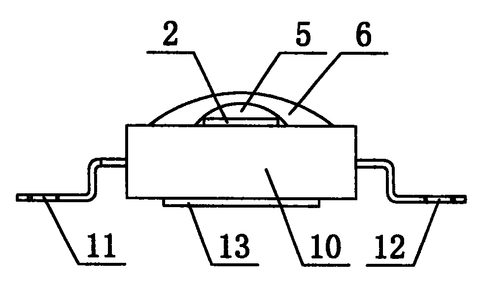
图1a是本实用新型实施例一、二、三贴片式发光二极管的侧面结构示意图;Fig. 1a is a schematic diagram of the side structure of the first, second and third patch-type light-emitting diodes of the utility model;
图1b是本实用新型实施例四、五、六贴片式发光二极管的侧面结构示意图;Fig. 1b is a schematic diagram of the side structure of the fourth, fifth and sixth patch-type light-emitting diodes of the utility model;
图2是本实用新型支架的立体结构示意图;Fig. 2 is the three-dimensional structure schematic diagram of the utility model support;
图3是本实用新型实施例一LED芯片的正面结构示意图;Fig. 3 is a schematic diagram of the front structure of an LED chip according to
图4是图3所示LED芯片的A-A断面结构示意图;Fig. 4 is a schematic diagram of the A-A section structure of the LED chip shown in Fig. 3;
图5是本实用新型实施例二LED芯片的正面结构示意图;Fig. 5 is a schematic diagram of the front structure of the LED chip of the second embodiment of the utility model;
图6是图5所示LED芯片的B-B断面结构示意图;Fig. 6 is a schematic diagram of the B-B cross-sectional structure of the LED chip shown in Fig. 5;
图7是本实用新型实施例三LED芯片的正面结构示意图;Fig. 7 is a schematic diagram of the front structure of the LED chip of the third embodiment of the utility model;
图8是图7所示LED芯片的C-C断面结构示意图;Fig. 8 is a schematic diagram of the C-C section structure of the LED chip shown in Fig. 7;
图9是本实用新型实施例四LED芯片的正面结构示意图;Fig. 9 is a schematic diagram of the front structure of the LED chip of the fourth embodiment of the utility model;
图10是图9所示LED芯片的D-D断面结构示意图;Fig. 10 is a schematic diagram of a D-D cross-sectional structure of the LED chip shown in Fig. 9;
图11是本实用新型实施例五LED芯片的正面结构示意图;Fig. 11 is a schematic diagram of the front structure of the LED chip according to
图12是图11所示LED芯片的E-E断面结构示意图;Fig. 12 is a schematic diagram of the E-E section structure of the LED chip shown in Fig. 11;
图13是本实用新型实施例六LED芯片的正面结构示意图;Fig. 13 is a schematic diagram of the front structure of the LED chip of the sixth embodiment of the utility model;
图14是图13所示贴片式发光二极管的F-F断面结构示意图;Fig. 14 is a schematic diagram of the F-F cross-sectional structure of the patch type light-emitting diode shown in Fig. 13;
图15是本实用新型贴片式发光二极管制造过程中LED芯片与框架的连接结构示意图。Fig. 15 is a schematic diagram of the connection structure between the LED chip and the frame during the manufacturing process of the patch type light emitting diode of the present invention.
具体实施方式 Detailed ways
实施例一:Embodiment one:
如图1a、图2、图3、图4所示,本实施例的贴片式发光二极管包括支架1、LED芯片2、覆盖于所述LED芯片2上的荧光粉5、保护胶6,所述保护胶6采用硅胶或树脂,所述支架1包括壳体10、两个引脚11、12、散热柱13,所述壳体10采用绝缘材料制成,所述散热柱13嵌入所述壳体10且上下贯穿所述壳体10。所述LED芯片2为正装LED集成芯片,包括硅衬底20、阳极接点21、阴极接点22和12个LED裸芯片23,所述硅衬底20固定于所述散热柱13上,所述阳极接点21、所述阴极接点22分别通过金属引线与两个所述引脚11、12相连接,所述LED裸芯片23之间采用先每三个并联成一组,再将四组相串联连接的连接方式,这样,所述阳极接点21、所述阴极接点22之间的额定电压是单个LED裸芯片的4倍,即可以直接接于12V直流电源上,因此可应用于汽车上作为光源,而不需要外围电路,因此使用方便,连接简单,故障率低,节省功耗。所述LED裸芯片23包括砷化镓(GaAs)衬底230和N型外延层231、P型外延层232,当然,所述衬底230也可以为碳化硅(SiC)衬底,即所述LED裸芯片23为单电极芯片,所述硅衬底20为N型硅衬底,所述硅衬底20顶面于每个所述LED裸芯片23处有两个分离的沉积金属层24,所述LED裸芯片23正装焊接在各所述金属层24上,即所述衬底230直接焊接在所述金属层24上,所述P型外延层232通过金属线41对应焊接在相邻的一个所述金属层24上,所述硅衬底20于每个所述LED裸芯片23处有一个P型阱区27,所述金属层24与所述硅衬底20的结合区分别还有一个掺杂磷或砷等材料的N型隔离层25,所述隔离层25位于所述阱区27内,用于隔离所述金属层24与所述硅衬底20,防止所述金属层24之间漏电或短路,同时所述隔离层25将所述LED裸芯片23传给所述金属层24的热量再传递给所述硅衬底20,起到良好的导热、散热作用,另外所述隔离层25与其所在的所述阱区27之间也构成一个静电保护二极管,起到在封装过程中静电保护的作用,各所述LED裸芯片23对应的所述金属层24之间设有阻挡层26,防止所述金属层24之间漏电或短路,所述金属层24分别引出所述阳极接点21、所述阴极接点22。所述金属层24为金属铝,当然也可以采用金属铜或硅铝合金,所述金属层24既是电极、导电体,又是散热片,所述金属线41为金线,当然也可以为铝线或铜线。As shown in Fig. 1a, Fig. 2, Fig. 3, and Fig. 4, the patch type light-emitting diode of this embodiment includes a
当然,所述硅衬底20也可以为P型硅衬底,此时,所述阱区27为N型阱区,所述隔离层25为掺杂硼或二氟化硼等材料的P型隔离层。Of course, the
本实施例的贴片式发光二极管的制造方法包括以下步骤:The manufacturing method of the patch type light-emitting diode of the present embodiment comprises the following steps:
(a)制作框架:如图15所示,在同一片镂空金属框架8上形成两列纵横均布排列的所述支架1,每个所述支架1的所述壳体10通过四条细连接筋81与所述框架8相连接,以便将所述支架1成版并规则定位;(a) Make frame: as shown in Figure 15, form two rows of vertically and horizontally uniformly arranged supports 1 on the same
(b)上芯片:将所述LED芯片2的所述硅衬底20固定于所述上散热柱13上;(b) Upper chip: fixing the
(c)打线:将所述LED芯片2的所述阳极接点21、所述阴极接点22分别与两个所述引脚11、12通过打线相固定连接;(c) Wire bonding: the
(d)上荧光粉:将所述荧光粉5覆盖于所述LED芯片2上;(d) phosphor powder: covering the
(e)上保护胶:将硅胶或树脂作为所述保护胶6直接覆盖于所述壳体10上部;(e) Upper protective glue: use silica gel or resin as the
(f)弯脚:将所述引脚11、12折弯成型,使其与使用状态形状一致,便于安装;(f) Bending feet: the
(g)切筋:将所述壳体10与所述框架8相连接的所述筋81切断,使成版的所述贴片式发光二极管成为各个独立元件。(g) Rib cutting: cutting the
实施例二:Embodiment two:
如图5、图6所示,本实施例与实施例一的不同之处在于:本实施例的贴片式发光二极管的所述LED芯片2为倒装LED集成芯片,所述P型外延层232、所述N型外延层231分别通过焊球42倒装焊接在所述金属层24上,所述焊球42为金球栓,当然也可以为铜球栓或锡球。As shown in Figure 5 and Figure 6, the difference between this embodiment and
本实施例其余特征与实施例一相同。The remaining features of this embodiment are the same as those of
实施例三:Embodiment three:
如图7、图8所示,本实施例与实施例一的不同之处在于:本实施例的贴片式发光二极管的所述衬底230为氧化铝(Al2O3)衬底,即所述LED裸芯片23为双电极芯片,所述衬底230正装焊接或粘贴在所述金属层24上,所述P型外延层232、所述N型外延层231分别通过金属线43、45焊接在相邻的所述金属层24上。As shown in Fig. 7 and Fig. 8, the difference between the present embodiment and the first embodiment is that the
本实施例其余特征与实施例一相同。The remaining features of this embodiment are the same as those of
实施例四:Embodiment four:
如图1b、图9、图10所示,本实施例与实施例一的不同之处在于:各所述LED裸芯片23之间通过所述金属层24的连接方式——本实施例各所述LED裸芯片23之间全部相串联连接,即所述阳极接点21和所述阴极接点22之间的所有LED裸芯片23相串联,这样,所述阳极接点21、所述阴极接点22之间的额定电压是单个LED裸芯片的12倍,即可以直接接于36~40V直流电源上,同样不需要外围电路。另外,本实施例所述贴片式发光二极管还包括光学透镜14,所述光学透镜14包罩于所述LED芯片2的外部且所述光学透镜14内部充满所述保护胶6,所述光学透镜14可采用多种角度,以提高聚光效果。As shown in Figure 1b, Figure 9, and Figure 10, the difference between this embodiment and
由此,本实施例贴片式发光二极管的制造方法在步骤(e)中还包括安装光学透镜,即将所述光学透镜14固定于所述壳体10上,并将所述保护胶6填充注满于所述光学透镜14内。Therefore, the manufacturing method of the chip-type light-emitting diode of this embodiment further includes installing an optical lens in step (e), that is, fixing the
本实施例其余特征与实施例一相同。The remaining features of this embodiment are the same as those of
实施例五:Embodiment five:
如图11、图12所示,本实施例与实施例四的不同之处在于:本实施例的贴片式发光二极管的所述LED芯片2为倒装LED集成芯片,所述P型外延层232、所述N型外延层231分别通过焊球42倒装焊接在所述金属层24上,所述焊球42为金球栓,当然也可以为铜球栓或锡球。As shown in Figure 11 and Figure 12, the difference between this embodiment and Embodiment 4 is that: the
本实施例其余特征与实施例四相同。The rest of the features of this embodiment are the same as those of the fourth embodiment.
实施例六:Embodiment six:
如图13、图14所示,本实施例与实施例四的不同之处在于:本实施例的贴片式发光二极管的所述衬底230为氧化铝(Al2O3)衬底,即所述LED裸芯片23为双电极芯片,所述衬底230正装焊接或粘贴在所述金属层24上,所述P型外延层232、所述N型外延层231分别通过金属线43、45焊接在相邻的所述金属层24上。As shown in Fig. 13 and Fig. 14, the difference between this embodiment and Embodiment 4 is that: the
本实施例其余特征与实施例四相同。The rest of the features of this embodiment are the same as those of the fourth embodiment.
当然,本实用新型贴片式发光二极管所述LED裸芯片23的具体连接方式和数量不限于以上实施例,实施例中仅是举例说明。比如,可根据实际需要,将12个所述LED裸芯片23之间采用先每两个并联成一组,再将六组相串联连接的连接方式,这样,可以直接接于18~20V直流电源上使用;还可以将40个所述LED裸芯片23之间全部相串联连接,这样,可以直接接于120V直流电源上使用。Certainly, the specific connection method and quantity of the LED
本实用新型将若干个所述LED裸芯片23正装或倒装集成在一个所述硅衬底20上,并将所述LED芯片2连接在所述支架1上,使得单个LED额定电压高,可直接与电压较高的电源相连接,而不需要外围电路,连接简单,故障率低,且散热效果好,功耗低,使用寿命长。The utility model integrates a plurality of said
本实用新型可广泛应用于LED照明领域。The utility model can be widely used in the field of LED lighting.
Claims (6)
Priority Applications (1)
| Application Number | Priority Date | Filing Date | Title |
|---|---|---|---|
| CNU2007200517920U CN201069771Y (en) | 2007-05-23 | 2007-05-23 | SMD LED |
Applications Claiming Priority (1)
| Application Number | Priority Date | Filing Date | Title |
|---|---|---|---|
| CNU2007200517920U CN201069771Y (en) | 2007-05-23 | 2007-05-23 | SMD LED |
Publications (1)
| Publication Number | Publication Date |
|---|---|
| CN201069771Y true CN201069771Y (en) | 2008-06-04 |
Family
ID=39491160
Family Applications (1)
| Application Number | Title | Priority Date | Filing Date |
|---|---|---|---|
| CNU2007200517920U Expired - Lifetime CN201069771Y (en) | 2007-05-23 | 2007-05-23 | SMD LED |
Country Status (1)
| Country | Link |
|---|---|
| CN (1) | CN201069771Y (en) |
Cited By (3)
| Publication number | Priority date | Publication date | Assignee | Title |
|---|---|---|---|---|
| CN101872828A (en) * | 2010-06-21 | 2010-10-27 | 深圳雷曼光电科技股份有限公司 | A packaging method for flip-chip LED chips |
| CN105514056A (en) * | 2016-01-15 | 2016-04-20 | 中山芯达电子科技有限公司 | A Chip Packaging Structure Facilitating Heat Dissipation |
| CN105679737A (en) * | 2016-01-15 | 2016-06-15 | 中山芯达电子科技有限公司 | A multi-chip packaging structure |
-
2007
- 2007-05-23 CN CNU2007200517920U patent/CN201069771Y/en not_active Expired - Lifetime
Cited By (4)
| Publication number | Priority date | Publication date | Assignee | Title |
|---|---|---|---|---|
| CN101872828A (en) * | 2010-06-21 | 2010-10-27 | 深圳雷曼光电科技股份有限公司 | A packaging method for flip-chip LED chips |
| CN101872828B (en) * | 2010-06-21 | 2012-07-25 | 深圳雷曼光电科技股份有限公司 | Packaging method for flip LED chips |
| CN105514056A (en) * | 2016-01-15 | 2016-04-20 | 中山芯达电子科技有限公司 | A Chip Packaging Structure Facilitating Heat Dissipation |
| CN105679737A (en) * | 2016-01-15 | 2016-06-15 | 中山芯达电子科技有限公司 | A multi-chip packaging structure |
Similar Documents
| Publication | Publication Date | Title |
|---|---|---|
| CN100508186C (en) | Surface mount light emitting type and preparation method thereof | |
| TW535307B (en) | Package of light emitting diode with protective diode | |
| US7391153B2 (en) | Light emitting device provided with a submount assembly for improved thermal dissipation | |
| CN201363572Y (en) | LED light source module | |
| TWI528508B (en) | High-power light-emitting diode ceramic package manufacturing method | |
| CN201412704Y (en) | A light source with integrated LED chips | |
| TW201143023A (en) | Light emitting diode package, lighting device and light emitting diode package substrate | |
| CN101958389A (en) | LED surface mounting structure for silicon substrate integrated with functional circuits and packaging method thereof | |
| TW201101548A (en) | LED package structure with a plurality of standby pads for increasing wire-bonding yield and method for manufacturing the same | |
| CN101154656B (en) | Multi-chip light-emitting diode module structure and manufacturing method thereof | |
| WO2008056813A1 (en) | Light emitting device and method for manufacturing the same | |
| US20120043886A1 (en) | Integrated Heat Conductive Light Emitting Diode (LED) White Light Source Module | |
| CN107393911B (en) | An energy-saving RGB-LED package, package module and display screen | |
| KR101181224B1 (en) | Led package and fabricating method of the same | |
| TWI447975B (en) | Structure of light-emitting diode chip, structure of light-emitting diode package substrate, light-emitting diode package structure and preparation method thereof | |
| CN102364685A (en) | Lead-free LED (Light-Emitting Diode) module and manufacturing process thereof | |
| CN201904368U (en) | LED (light emitting diode) surface-mounting package structure based on silicon substrate integrated with functional circuit | |
| CN100554773C (en) | A LED lamp with heat dissipation aluminum plate | |
| CN102468293A (en) | Polycrystal packaging structure directly electrically connected with alternating current power supply | |
| CN105609496A (en) | High power density COB (Chip On Board) packaged white LED (Light Emitting Diode) module and packaging method thereof | |
| CN113097366A (en) | Inverted double-sided packaging full-circumference light-emitting LED bracket and preparation method thereof | |
| CN201093214Y (en) | Direct inserting type LED | |
| KR20130077059A (en) | Led package and manufacturing method for the same | |
| CN202049955U (en) | Polycrystalline package structure for increasing the amount of current using a constant voltage power supply | |
| CN207883721U (en) | A kind of LED light bar with excellent heat dispersion performance |
Legal Events
| Date | Code | Title | Description |
|---|---|---|---|
| C14 | Grant of patent or utility model | ||
| GR01 | Patent grant | ||
| AV01 | Patent right actively abandoned |
Effective date of abandoning: 20070523 |
|
| AV01 | Patent right actively abandoned |
Effective date of abandoning: 20070523 |
|
| C25 | Abandonment of patent right or utility model to avoid double patenting |