CN1928981A - Driver for display apparatus and display apparatus including the same - Google Patents
Driver for display apparatus and display apparatus including the same Download PDFInfo
- Publication number
- CN1928981A CN1928981A CNA2006101269326A CN200610126932A CN1928981A CN 1928981 A CN1928981 A CN 1928981A CN A2006101269326 A CNA2006101269326 A CN A2006101269326A CN 200610126932 A CN200610126932 A CN 200610126932A CN 1928981 A CN1928981 A CN 1928981A
- Authority
- CN
- China
- Prior art keywords
- clock signal
- signal
- voltage
- driver
- pixel
- Prior art date
- Legal status (The legal status is an assumption and is not a legal conclusion. Google has not performed a legal analysis and makes no representation as to the accuracy of the status listed.)
- Pending
Links
Images


Classifications
-
- G—PHYSICS
- G09—EDUCATION; CRYPTOGRAPHY; DISPLAY; ADVERTISING; SEALS
- G09G—ARRANGEMENTS OR CIRCUITS FOR CONTROL OF INDICATING DEVICES USING STATIC MEANS TO PRESENT VARIABLE INFORMATION
- G09G3/00—Control arrangements or circuits, of interest only in connection with visual indicators other than cathode-ray tubes
- G09G3/20—Control arrangements or circuits, of interest only in connection with visual indicators other than cathode-ray tubes for presentation of an assembly of a number of characters, e.g. a page, by composing the assembly by combination of individual elements arranged in a matrix no fixed position being assigned to or needed to be assigned to the individual characters or partial characters
- G09G3/34—Control arrangements or circuits, of interest only in connection with visual indicators other than cathode-ray tubes for presentation of an assembly of a number of characters, e.g. a page, by composing the assembly by combination of individual elements arranged in a matrix no fixed position being assigned to or needed to be assigned to the individual characters or partial characters by control of light from an independent source
- G09G3/36—Control arrangements or circuits, of interest only in connection with visual indicators other than cathode-ray tubes for presentation of an assembly of a number of characters, e.g. a page, by composing the assembly by combination of individual elements arranged in a matrix no fixed position being assigned to or needed to be assigned to the individual characters or partial characters by control of light from an independent source using liquid crystals
- G09G3/3611—Control of matrices with row and column drivers
- G09G3/3674—Details of drivers for scan electrodes
- G09G3/3677—Details of drivers for scan electrodes suitable for active matrices only
-
- G—PHYSICS
- G02—OPTICS
- G02F—OPTICAL DEVICES OR ARRANGEMENTS FOR THE CONTROL OF LIGHT BY MODIFICATION OF THE OPTICAL PROPERTIES OF THE MEDIA OF THE ELEMENTS INVOLVED THEREIN; NON-LINEAR OPTICS; FREQUENCY-CHANGING OF LIGHT; OPTICAL LOGIC ELEMENTS; OPTICAL ANALOGUE/DIGITAL CONVERTERS
- G02F1/00—Devices or arrangements for the control of the intensity, colour, phase, polarisation or direction of light arriving from an independent light source, e.g. switching, gating or modulating; Non-linear optics
- G02F1/01—Devices or arrangements for the control of the intensity, colour, phase, polarisation or direction of light arriving from an independent light source, e.g. switching, gating or modulating; Non-linear optics for the control of the intensity, phase, polarisation or colour
- G02F1/13—Devices or arrangements for the control of the intensity, colour, phase, polarisation or direction of light arriving from an independent light source, e.g. switching, gating or modulating; Non-linear optics for the control of the intensity, phase, polarisation or colour based on liquid crystals, e.g. single liquid crystal display cells
-
- G—PHYSICS
- G09—EDUCATION; CRYPTOGRAPHY; DISPLAY; ADVERTISING; SEALS
- G09G—ARRANGEMENTS OR CIRCUITS FOR CONTROL OF INDICATING DEVICES USING STATIC MEANS TO PRESENT VARIABLE INFORMATION
- G09G3/00—Control arrangements or circuits, of interest only in connection with visual indicators other than cathode-ray tubes
- G09G3/20—Control arrangements or circuits, of interest only in connection with visual indicators other than cathode-ray tubes for presentation of an assembly of a number of characters, e.g. a page, by composing the assembly by combination of individual elements arranged in a matrix no fixed position being assigned to or needed to be assigned to the individual characters or partial characters
- G09G3/34—Control arrangements or circuits, of interest only in connection with visual indicators other than cathode-ray tubes for presentation of an assembly of a number of characters, e.g. a page, by composing the assembly by combination of individual elements arranged in a matrix no fixed position being assigned to or needed to be assigned to the individual characters or partial characters by control of light from an independent source
- G09G3/36—Control arrangements or circuits, of interest only in connection with visual indicators other than cathode-ray tubes for presentation of an assembly of a number of characters, e.g. a page, by composing the assembly by combination of individual elements arranged in a matrix no fixed position being assigned to or needed to be assigned to the individual characters or partial characters by control of light from an independent source using liquid crystals
- G09G3/3611—Control of matrices with row and column drivers
- G09G3/3648—Control of matrices with row and column drivers using an active matrix
-
- G—PHYSICS
- G11—INFORMATION STORAGE
- G11C—STATIC STORES
- G11C19/00—Digital stores in which the information is moved stepwise, e.g. shift registers
- G11C19/28—Digital stores in which the information is moved stepwise, e.g. shift registers using semiconductor elements
-
- G—PHYSICS
- G09—EDUCATION; CRYPTOGRAPHY; DISPLAY; ADVERTISING; SEALS
- G09G—ARRANGEMENTS OR CIRCUITS FOR CONTROL OF INDICATING DEVICES USING STATIC MEANS TO PRESENT VARIABLE INFORMATION
- G09G2300/00—Aspects of the constitution of display devices
- G09G2300/04—Structural and physical details of display devices
- G09G2300/0421—Structural details of the set of electrodes
- G09G2300/0426—Layout of electrodes and connections
-
- G—PHYSICS
- G09—EDUCATION; CRYPTOGRAPHY; DISPLAY; ADVERTISING; SEALS
- G09G—ARRANGEMENTS OR CIRCUITS FOR CONTROL OF INDICATING DEVICES USING STATIC MEANS TO PRESENT VARIABLE INFORMATION
- G09G2310/00—Command of the display device
- G09G2310/02—Addressing, scanning or driving the display screen or processing steps related thereto
- G09G2310/0243—Details of the generation of driving signals
- G09G2310/0251—Precharge or discharge of pixel before applying new pixel voltage
-
- G—PHYSICS
- G09—EDUCATION; CRYPTOGRAPHY; DISPLAY; ADVERTISING; SEALS
- G09G—ARRANGEMENTS OR CIRCUITS FOR CONTROL OF INDICATING DEVICES USING STATIC MEANS TO PRESENT VARIABLE INFORMATION
- G09G2310/00—Command of the display device
- G09G2310/08—Details of timing specific for flat panels, other than clock recovery
-
- G—PHYSICS
- G09—EDUCATION; CRYPTOGRAPHY; DISPLAY; ADVERTISING; SEALS
- G09G—ARRANGEMENTS OR CIRCUITS FOR CONTROL OF INDICATING DEVICES USING STATIC MEANS TO PRESENT VARIABLE INFORMATION
- G09G2320/00—Control of display operating conditions
- G09G2320/02—Improving the quality of display appearance
- G09G2320/0209—Crosstalk reduction, i.e. to reduce direct or indirect influences of signals directed to a certain pixel of the displayed image on other pixels of said image, inclusive of influences affecting pixels in different frames or fields or sub-images which constitute a same image, e.g. left and right images of a stereoscopic display
-
- G—PHYSICS
- G09—EDUCATION; CRYPTOGRAPHY; DISPLAY; ADVERTISING; SEALS
- G09G—ARRANGEMENTS OR CIRCUITS FOR CONTROL OF INDICATING DEVICES USING STATIC MEANS TO PRESENT VARIABLE INFORMATION
- G09G3/00—Control arrangements or circuits, of interest only in connection with visual indicators other than cathode-ray tubes
- G09G3/20—Control arrangements or circuits, of interest only in connection with visual indicators other than cathode-ray tubes for presentation of an assembly of a number of characters, e.g. a page, by composing the assembly by combination of individual elements arranged in a matrix no fixed position being assigned to or needed to be assigned to the individual characters or partial characters
- G09G3/34—Control arrangements or circuits, of interest only in connection with visual indicators other than cathode-ray tubes for presentation of an assembly of a number of characters, e.g. a page, by composing the assembly by combination of individual elements arranged in a matrix no fixed position being assigned to or needed to be assigned to the individual characters or partial characters by control of light from an independent source
- G09G3/36—Control arrangements or circuits, of interest only in connection with visual indicators other than cathode-ray tubes for presentation of an assembly of a number of characters, e.g. a page, by composing the assembly by combination of individual elements arranged in a matrix no fixed position being assigned to or needed to be assigned to the individual characters or partial characters by control of light from an independent source using liquid crystals
- G09G3/3611—Control of matrices with row and column drivers
- G09G3/3614—Control of polarity reversal in general
Abstract
Provided is a driver for a display apparatus and a display apparatus having the same. The driver includes a plurality of gate lines that transmit gate signals, and first and second gate drivers that are respectively connected to odd-numbered and even-numbered gate lines among the plurality of gate lines and generate the gate signals based on a plurality of clock signals, wherein two adjacent clock signals among the plurality of clock signals have a phase difference equal to or greater than 180 DEG and less than 360 DEG . Accordingly, voltage drop caused by a kickback voltage occurs only one time by allowing two adjacent clock signals to have a predetermined time delay from each other, so that a positive data voltage is the same as a negative data voltage, thereby preventing flicker or stain.
Description
The present invention requires the right of priority of the korean patent application submitted to Korea S Department of Intellectual Property on September 7th, 2005 2005-0083039 number, and its full content is hereby expressly incorporated by reference.
Technical field
The present invention relates to a kind of driver and a kind of display device that is used for display device with this driver.
Background technology
In general, liquid crystal display (LCD) device comprises that two are provided with the panel of pixel electrode and common electrode and are arranged on the liquid crystal layer that has dielectric anisotropy between two panels.Pixel electrode is arranged with matrix form.Pixel electrode is connected to the on-off element such as thin film transistor (TFT) (" TFT "), thus with pixel behavior unit sequence be applied in data voltage.Common electrode is arranged on the top on the whole surface of panel, and has been applied in the common-battery pressure.According to circuit theory, pixel electrode, common electrode and intervenient liquid crystal layer are formed liquid
Become liquid crystal capacitor.Liquid crystal capacitor is formed pixel cell with the on-off element that is connected in this.
In liquid crystal indicator, two electrodes (for example, pixel electrode and common electrode) are applied voltage, in liquid crystal layer, to generate electric field.Optical transmission rate by the intensity adjustments of control electric field is passed liquid crystal layer obtains desired images.If in one direction liquid crystal layer is applied voltage in very long a period of time, deterioration can take place in picture quality.Therefore, need be unit presses reversal data voltage with respect to the common-battery that imposes on common electrode polarity with frame, pixel column or pixel.
Liquid crystal indicator comprises: gate drivers is used for gating signal is transferred to gate line, to open or to close the on-off element of each pixel; Grayscale voltage generator is used to generate a plurality of grayscale voltages; Data driver is used for choosing voltage corresponding to view data from grayscale voltage, and data voltage is imposed on data line in the display signal line; And signal controller, be used to control these parts.
Form gate drivers with the technology identical, subsequently gate drivers is integrated in the panel with the on-off element that is used to form pixel.Reduce the quantity of data line by reducing by half, rather than the quantity of gate line is doubled, thereby realized identical resolution and reduced cost.In addition, on the left side and the right side of panel a pair of relative gate drivers is set, to apply gating signal.In order to apply gating signal in an image duration, after applying last gating signal, by through after the schedule time with next gating signal and overlapping next gating signal of transmitting of last gating signal.
When signal wire is overlapping, in pixel, form stray capacitance.After applying data voltage, because at the Kickback voltage (kickback voltage) that negative edge generated, data voltage reduces slightly, after this by stray capacitance, because at the Kickback voltage that negative edge generated of next gating signal, data voltage reduces once more.So just cause the voltage difference between positive pixel voltage and the negative pixel voltage, thereby cause flicker.In addition, because residual image or fingerprint may make screen produce spot (stain).
Therefore, a kind of driver that is used for display device and a kind of display device that can prevent screen flicker or spot of expectation with this driver.
Summary of the invention
The object of the invention is to provide a kind of driver and a kind of display device with this driver that is used for display device, and it has the advantage of screen flicker of preventing or pollution.
Exemplary embodiment of the present invention provides a kind of driver that is used for display device.
According to exemplary embodiment of the present invention, the driver that is used for display device comprises: many gate lines are used to transmit gating signal; And first and second gate drivers, being connected to the odd and even number gate line in many gate lines respectively, first and second gate drivers generate gating signals based on a plurality of clock signals.Two adjacent clock signals in a plurality of clock signals have and are equal to or greater than 180 ° and less than 360 ° phase differential.
In addition, two non-conterminous clock signals in a plurality of clock signals can have 180 ° phase differential.
A plurality of clock signals all can have 50% dutycycle.
A plurality of clock signals comprise first to fourth clock signal, and first and second clock signals or third and fourth clock signal can have and be equal to or greater than 180 ° and less than 360 ° phase differential.
The first and the 3rd clock signal or the second and the 4th clock signal can have 180 ° phase differential.
The first and the 3rd clock signal can input to the first grid driver, the second and the 4th clock signal can input to the second grid driver, the first and second output start signals can input to first and second gate drivers respectively, and the first and second output start signals can have and are equal to or greater than 180 ° and less than 360 ° phase differential.
Another exemplary embodiment of the present invention provides a kind of display device, and it comprises: a plurality of pixels are arranged; Many gate lines are used for gating signal is transferred to pixel; Many data lines are used for data signal transmission to pixel; And first and second gate drivers, being connected to the odd and even number gate line in many gate lines respectively, first and second gate drivers generate gating signals based on a plurality of clock signals.Two adjacent clock signals in a plurality of clock signals have and are equal to or greater than 180 ° and less than 360 ° phase differential.
In addition, two non-conterminous clock signals in a plurality of clock signals can have 180 ° phase differential.
A plurality of clock signals all can have 50% dutycycle.
A plurality of clock signals can comprise first to fourth clock signal, and first and second clock signals or third and fourth clock signal can have and be equal to or greater than 180 ° and less than 360 ° phase differential.
The first and the 3rd clock signal or the second and the 4th clock signal can have 180 ° phase differential.
The first and the 3rd clock signal can input to the first grid driver, and the second and the 4th clock signal can input to the second grid driver.
The first and second output start signals can input to first and second gate drivers respectively, and the first and second output start signals can have and are equal to or greater than 180 ° and less than 360 ° phase differential.
Two adjacent pixels (a pair of neighbor) that follow the direction setting between two adjacent data lines in a plurality of pixels can be connected to identical data line, and these two pixels can be connected to the gate line that differs from one another.
Display device can also comprise the data driver that is used to generate data-signal, wherein, data driver imposes on pixel with data-signal, and this pixel at first receives the data-signal between two adjacent pixels of first pixel column in a plurality of pixel columns of arranging along column direction.
First second grid driver can be integrated in the display device.
Description of drawings
Describe exemplary embodiment in further detail by the reference accompanying drawing, above-mentioned and further feature of the present invention and advantage will become apparent, wherein:
Fig. 1 illustrates the block diagram of liquid crystal indicator according to an exemplary embodiment of the present invention;
Fig. 2 illustrates the schematic equivalent circuit of the pixel of liquid crystal indicator according to an exemplary embodiment of the present invention;
Fig. 3 illustrates the structure of liquid crystal indicator according to an exemplary embodiment of the present invention;
Fig. 4 is the block diagram of gate drivers according to an exemplary embodiment of the present invention;
Fig. 5 is the circuit diagram of j level that is used for the shift register of gate drivers according to an exemplary embodiment of the present invention;
Fig. 6 A and 6B illustrate the signal waveform of the gate drivers of Fig. 4;
Fig. 7 A and 7B illustrate respectively according to the gating signal of exemplary embodiment of the present invention and prior art and the waveform of data voltage; And
Fig. 8 illustrates the portion waveshape of the gating signal output of gate drivers according to an exemplary embodiment of the present invention.
Embodiment
The present invention is more comprehensively described below with reference to accompanying drawings.Yet the present invention can realize with different ways, and be not limited to embodiment described here.On the contrary, to one skilled in the art, provide these embodiment, make that the present invention is fully open and cover scope of the present invention fully.Identical label is represented similar elements.
Should be understood that it can be located immediately on other element or also can exist insertion element when mentioning element and " be positioned at " on another element.On the contrary, when mentioning element and " be located immediately at " on another element, there is not insertion element.At this, term " and/or " comprise one or more relevant listed terms arbitrarily and all combinations.
Although should be appreciated that at this and may use the term first, second, third, etc. to describe different elements, parts, zone, layer and/or portion, these elements, parts, zone, layer and/or portion are not limited to these terms.These terms only are used for element, parts, zone, layer or a portion are distinguished mutually with another zone, layer or portion.Therefore, under the situation that does not deviate from aim of the present invention, hereinafter described first element, parts, zone, layer or portion can be called second element, parts, zone, layer or portion.
Term only is used to describe specific embodiment rather than restriction the present invention as used herein.As used herein, " one " of singulative, " this " also comprise plural form, unless there is other clearly to indicate in the literary composition in addition.Should further understand, when in present specification, using term " to comprise " and/or when " comprising ", be meant feature, zone, integer, step, operation, element and/or parts that existence is claimed, do not exist or additional one or more other feature, zone, integer, step, operation, element, parts and/or its combination but do not get rid of also.
In addition, this may use such as " ... under ", " ... following ", " following ", " ... top " and spatial relationship terms such as " top ", with describe as shown in FIG. an element and the relation of another element.Should be appreciated that except that the orientation shown in the figure, the spatial relationship term will comprise the different azimuth of device.For example, if the device among the width of cloth figure that overturns, the element that then is described as be in other elements " following " will be positioned in " top " of other elements.Therefore, exemplary term " ... following " can be included in according to the particular orientation of figure above and below orientation.Similarly, if the device among the width of cloth figure that overturns, then be described as be in other element " following " or " under " element will be positioned in " top " of other element.Therefore, exemplary term " following " or " under " can comprise above and following orientation.
Unless special the qualification has the common explanation of understanding equivalent in meaning with those skilled in the art at these employed all terms (comprising technical term and scientific and technical terminology).It should also be further understood that, should be interpreted as such as defined term in general dictionary consistent with its meaning in the correlation technique context, unless and limit especially at this, should Utopian or too formal it not be made an explanation.
Below, the present invention is described with reference to the accompanying drawings.
At first, with reference to Fig. 1 to Fig. 3 with liquid crystal indicator as case description liquid crystal indicator according to an exemplary embodiment of the present invention.
Fig. 1 illustrates the block diagram of liquid crystal indicator according to an exemplary embodiment of the present invention.Fig. 2 illustrates the schematic equivalent circuit of the pixel of liquid crystal indicator according to an exemplary embodiment of the present invention.Fig. 3 illustrates the structure of liquid crystal indicator according to an exemplary embodiment of the present invention.
As shown in Figure 1, the liquid crystal indicator signal controller 600 that comprises liquid crystal panel assembly 300, be connected to the gate drivers 400L of liquid crystal panel assembly 300 and 400R and data driver 500, be connected to the grayscale voltage generator 800 of data driver 500 and be used to control these parts according to an exemplary embodiment of the present invention.
Can find out well that from Fig. 1 and Fig. 3 liquid crystal panel assembly 300 comprises many signal line G
1To G
2n, D
1To D
m, L1 and L2.In addition, a plurality of pixels that are connected to signal wire are arranged basically.
Signal wire G
1To G
2n, D
1To D
m, L1 and L2 comprise: many gate lines G
1To G
2n, be used to transmit gating signal (being sometimes referred to as " sweep signal "); And many data line D
1To D
mWith pseudo-line (dummy line) L1 and L2, be used for transmission of data signals.Gate lines G
1To G
2nOn line direction, extend parallel to each other basically, and data line D
1To D
mBasically extend parallel to each other on column direction with pseudo-line L1 and L2.
As shown in Figure 3, printed circuit board (PCB) (" PCB ") 550 is arranged on and comprises gate lines G
1To G
2n, data line D
1To D
m, and the top of the liquid crystal panel assembly 300 of pseudo-line L1 and L2.PCB 550 comprises the circuit component such as the signal controller 600 that is used to drive liquid crystal indicator, driving voltage generator and grayscale voltage generator (all not shown).Pseudo-line L1 and L2 extend along column direction substantially parallel to each other at the Far Left and the rightmost of liquid crystal panel assembly 300 respectively, and basically with data line D
1To D
mParallel.
Liquid crystal panel assembly 300 and PCB 500 are electrically connected to each other and physical connection by flexible print circuit (FPC) substrate 510.
FPC substrate 510 is equipped with the data-driven integrated circuit chip 540 of forming data driver 500, and forms and have many data lines 521.Data line 521 is connected to the data line D that forms respectively on liquid crystal panel assembly 300 by contact site C1
1To D
m, to transmit corresponding data voltage.
In FPC substrate 510, form signal transmssion line 522a, 522b, 523a and 523b in the left and the rightest position of data-driven integrated circuit chip 540.Signal transmssion line 522a, 522b, 523a and 523b are connected to signal transmssion line 551a and the 551b that forms by the contact site C3 of correspondence in PCB550.
The signal transmssion line 522a that forms in FPC substrate 510 leftmost sides is connected to the data line D1 of the leftmost side by contact site C2, and is connected to signal transmssion line 551a and 523a by contact site C3, to be connected to pseudo-line L2 by contact site C1.
The signal transmssion line 523b that forms in substrate 510 rightmost sides is connected to the data line D of the rightmost side by contact site C2
m, and be connected to signal transmssion line 551b and 523a by contact site C3, to be connected to pseudo-line L1 by contact site C1.
As can be seen, each pixel includes and is connected to display signal line G from Fig. 2 and Fig. 3
1To G
2n, D
1To D
m, and the on-off element Q of pseudo-line L1 and L2, the liquid crystal capacitor Clc that is connected in this and holding capacitor Cst.Yet, can optionally holding capacitor Cst be omitted.
On-off element Q (for example, thin film transistor (TFT)) is arranged on the lower panel 100 of thin-film transistor display panel.As three ports (three-port) device, its control end is connected to gate lines G
1To G
2nOne of them, its input end is connected to data line D
1To D
mAnd pseudo-line L1 and L2 one of them, with and output terminal be connected to liquid crystal capacitor Clc and holding capacitor Cst.
The pixel electrode 191 that two ends of liquid crystal capacitor Clc are lower panel 100 and the common electrode 270 of upper panel 200, this upper panel is the common electrode panel.Be interposed in liquid crystal layer 3 between two electrodes 191 and 270 as dielectric element.Pixel electrode 191 is connected to on-off element Q, and common electrode 270 is arranged on the whole surface of upper panel 200, presses Vcom to receive common-battery.Be different from shown in Figure 2ly, common electrode 270 can be arranged on the lower panel 100, rather than is arranged on the upper panel 200, and in this case, at least one in two electrodes 191 and 270 can form with linear or bar shaped.
By with independent signal wire (not shown) be arranged on pixel electrode 191 overlapping holding capacitor Cst that have for the subsidiary function of liquid crystal capacitor Clc that construct on the lower panel 100, wherein, between independent signal wire and pixel electrode, be gripped with insulating part, and will press the predetermined voltage of Vcom to impose on independent signal wire such as common-battery.Alternatively, can wherein, between pixel electrode and first previous gate line, be gripped with insulating part by pixel electrode 191 and side's disposed thereon first previous gate line being carried out the overlapping holding capacitor Cst that constructs.
As shown in Figure 3, pair of grid lines G
J+1And G
J+2, and G
J+3And G
J+4Be separately positioned on the above and below of the single row of pixel electrode 191.In addition, each bar data line D
1To D
mAll be arranged between two adjacent column of pixel electrode 191.Just, a data line is arranged between a pair of pixel column.Now, will describe gate lines G in detail
1To G
2nAnd connection between the pixel electrode 191 and data line D
1To D
mAnd the connection between the pixel electrode 191.
Be connected the many of pixel electrode 191 above and belows to gate lines G
1To G
2nThe on-off element Q of the above and below by being arranged on each pixel electrode 191 is connected in this.
Just, in the odd pixel row, be arranged on each bar data line D
1To D
mThe on-off element Q in left side is connected to upper gate line G
1, G
5..., G
4m+1, and be arranged on each bar data line D
1To D
mThe on-off element Q on right side is connected to the bottom gate lines G
2, G
6..., G
4m+2On the other hand, in the even pixel row, upper gate line G
3, G
7..., G
4m-1With the bottom gate lines G
4, G
8..., G
4mBe connected to on-off element Q in the mode opposite with respect to the odd pixel row.Just, be arranged on data line D
1To D
mThe on-off element Q on right side is connected to upper gate line G
3, G
7..., G
4m-1And be arranged on data line D
1To D
mThe on-off element Q in left side is connected to the bottom gate lines G
4, G
8..., G
4m
In odd-numbered line, be arranged on data line D
1To D
mThe pixel electrode 191 in left side is connected to the first adjacent data line D by its on-off element Q
1To D
mAnd be arranged on data line D
1To D
mThe pixel electrode 191 on right side is connected to the second adjacent data line D
1To D
mIn even number line, be arranged on data line D
1To D
mThe pixel electrode 191 in left side is connected to previous adjacent data line D by its on-off element Q
1To D
m, and be arranged on data line D
1To D
mThe pixel electrode 191 on right side is connected to the first adjacent data line D
1To D
mIn addition, the pixel electrode 191 in first row and even number line is connected to pseudo-line L1, and this puppet line is connected to the last item data line D
mAnd in the end one row and odd-numbered line in pixel electrode 191 be connected to pseudo-line L2, this puppet line is connected to article one data line D
1
As mentioned above, the on-off element Q that forms respectively in each pixel PX forms by this way: they can be connected to data line D easily
1To D
mOr pseudo-line L1 and L2, that is, they have short as far as possible connection distance.Therefore, in Fig. 3, on-off element Q is arranged on different positions in each pixel row and column.Just, odd pixel centering, be arranged on data line D
1To D
mThe upper right side of the pixel PX in left side forms on-off element Q, and is being arranged on data line D
1To D
mThe lower right side of the pixel PX on right side forms on-off element Q.
On the other hand, the on-off element Q that is arranged on the pixel PX in the even number line is formed on the position relative with respect to its adjacent lines of pixels.Just, even pixel centering, be arranged on data line D
1To D
mThe pixel PX in left side has its on-off element Q at lower left quarter, and is arranged on data line D
1To D
mThe pixel PX on right side has its on-off element Q at upper left quarter.
In simple terms, at pixel electrode 191 and the data line D of Fig. 3
1To D
mIn, the on-off element Q that is arranged on two pixel PX between two adjacent data lines of each pixel column is connected to identical data line.Just, in the odd pixel row, the on-off element Q of two pixel PX that form between two data lines is connected to the right side data line, and in the even pixel row, the on-off element Q of two pixel PX that form between two data lines is connected to the left data line.
The layout of Fig. 3 only is an example, therefore, and pixel electrode 191, odd and even number data line D
1To D
m, and data line G
1To G
2nCan connect in a different manner.
On the other hand, in order to realize colored demonstration, each pixel PX shows a kind of primary colors (space segmentation) uniquely, and perhaps each pixel PX is according to time-interleaved ground display primaries (time is cut apart).
Space or time combination by primary colors can obtain desired color.Fig. 2 illustrates the example of space segmentation, and wherein, in the zone corresponding to pixel electrode 191, each pixel PX includes red, green or blue color filter 230.Color filter 230 can be arranged on lower panel 100 tops as shown in Figure 2, or is arranged on lower panel 100 belows alternatively.
In Fig. 3, on line direction, be each color filter 230 that arranged in order is used for respective pixel PX with the redness in the primary colors, green and blueness, and each pixel column disposes linearly in the bar shaped mode, and wherein, each color filter 230 of pixel column only comprises a kind of color in the primary colors.
The outside surface of at least one is provided with the polarizer (not shown) that at least one is used to make light polarization in two panels 100 and 200.
Referring again to Fig. 1, two gray scale voltage group (benchmark gray scale group) that grayscale voltage generator 800 generates corresponding to the transmissivity of pixel PX.Gray scale group with respect to common-battery press Vcom have on the occasion of, and another gray scale voltage group presses Vcom to have negative value with respect to common-battery.
A pair of gate drivers 400L and 400R are separately positioned on the left side and the right side of liquid crystal panel assembly 300, and are connected to odd gates line G respectively
1, G
3..., G
2n-1With the even number gate lines G
2, G
4..., G
2n, so that gating signal is imposed on gate lines G
1To G
2n, wherein, gating signal is made up of external gate forward voltage Von and external gate cut-off voltage Voff.Gate drivers 400L and 400R comprise a plurality of levels (stage) that are the row arrangement basically, as shift register, and with the technology formation identical with the on-off element Q that forms pixel PX and integrated.Yet gate drivers 400L and 400R can be with the form settings of integrated circuit (" IC ").
Data driver 500 is connected to the data line D of liquid crystal panel assembly 300
1To D
m, from grayscale voltage generator 800, choosing grayscale voltage, and grayscale voltage is imposed on data line D as data-signal
1To D
mAlternatively, only generate the benchmark grayscale voltage of predetermined quantity rather than generate under the situation of all grayscale voltages at grayscale voltage generator 800, data driver 500 can generate grayscale voltage for all gray scales by dividing the benchmark grayscale voltage and choose data-signal in the grayscale voltage that generates.
Signal controller 600 control gate driver 400L and 400R, data driver 500 and grayscale voltage generator 800.
Each driver 500,600 and 800 all can one or more driving IC chip form be directly installed on the LCD panel assembly 300.Alternatively, driver 500,600 and 800 can be installed on flexible print circuit (" FPC ") the film (not shown) in the LCD panel assembly 300 with the form of carrying encapsulation (" TCP "), maybe can be installed in the independent printed circuit board (PCB) (not shown).Alternatively, driver 500,600 and 800 can with display signal line G
1To G
2nAnd D
1To D
m, and thin film transistor switch element Q be directly installed on together on the LCD panel assembly 300.
In addition, driver 400,500,600 and 800 can be integrated with the form of single chip, in this case, at least one driver or wherein at least one circuit component can appear at the outside of single chip.
The operation of liquid crystal indicator is described with reference to Fig. 1 now.
Signal controller 600 receives received image signal R, G and B and is used to control its demonstration from the external graphics controller (not shown) input control signal.As the example of input control signal, have vertical synchronizing signal Vsync, horizontal-drive signal Hsync, master clock signal MCLK and data enable signal DE.
Signal controller 600 is based on input control signal and received image signal R, G and B, operating conditions according to liquid crystal panel assembly 300 is handled received image signal R, G and B, to generate grid control signal CONT1, data controlling signal CONT2 etc., subsequently, the grid control signal CONT1 that generates is transferred to gate drivers 400L and 400R, and data controlling signal CONT2 and the processed images data DAT that generates transferred to data driver 500.
Grid control signal CONT1 comprises and is used for the clock signal that scanning start signal STV that beacon scanning begins and at least one are used to control the output cycle of gate-on voltage Von.Grid control signal CONT1 can also comprise the output enable signal OE of the duration that is used to limit gate-on voltage Von.
Data controlling signal CONT2 comprises: horizontal synchronization start signal STH is used for indicating the data transmission of (a pair of) pixel column; Load signal LOAD is used for order related data voltage is imposed on data line D
1To D
mAnd data clock signal HCLK.Data controlling signal CONT2 can also comprise reverse signal RVS, is used for pressing with respect to common-battery the polarity of voltage (hereinafter, " press the polarity of voltage of the data-signal of Vcom with respect to common-battery " and abbreviate " data-signal polarity " as) of Vcom inverted data signal.
In response to data controlling signal CONT2 from signal controller 600, data driver 500 receives the data image signal DAT of (a pair of) pixel column, and choose grayscale voltage corresponding to data image signal DAT, make data image signal DAT be converted into relevant analog data signal.Subsequently, simulating signal is applied in to relevant data line D
1To D
m
Impose on the voltage of data-signal of pixel PX and common-battery and press difference between the Vcom to become the charge voltage of liquid crystal capacitor Clc, that is, and pixel voltage.The orientation of liquid crystal molecule changes according to the intensity of pixel voltage.Therefore, changed the polarisation of light that passes liquid crystal layer 3.Because be attached to the polarizer of liquid crystal panel assembly 300, the change of polarization has caused the change of optical transmission rate.
(that is, the one-period of horizontal-drive signal Hsync and data enable signal DE) (or 1H) is unit with a horizontal cycle, repeats aforementioned operation, sequentially gate-on voltage Von is imposed on all gate lines G
1To G
2nThereby, data-signal is imposed on all pixels.As a result, the image that shows a frame.
When a frame end, next frame begins, and control imposes on the state of reverse signal RVS of data driver 500, makes the polarity of the data-signal that imposes on each pixel and polarity opposite (frame counter-rotating) in former frame.At this moment, even in a frame, according to the characteristic of reverse signal RVS, the polarity that flows through the data-signal of a data line also can be inverted (for example, row counter-rotating and some counter-rotating).In addition, the polarity that imposes on the data-signal of a pixel column can differ from one another (for example, row counter-rotating and some counter-rotating).
Now, with reference to Fig. 4 to Fig. 6 liquid crystal indicator is according to an exemplary embodiment of the present invention described.
Fig. 4 is the block diagram of gate drivers according to an exemplary embodiment of the present invention.Fig. 5 is the circuit diagram of j level that is used for the shift register of gate drivers according to an exemplary embodiment of the present invention.Fig. 6 A and 6B illustrate the signal waveform of the gate drivers of Fig. 4.
Gate drivers comprises the shift register 400L that is respectively Fig. 4 and first and second gate drivers 400L and the 400R of 400R.Shift register 400L and 400R receive first and second scanning start signal LSTV and RSTV and corresponding first to fourth clock signal LCLK1, RCLK1, LCLK2 and the RCLK2 respectively.Each shift register 400L and 400R include a plurality of grades of 410L and the 410R that is that row arrange, and among a plurality of grades of 410L and the 410R each is connected to corresponding gate line respectively.
As shown in Figure 6A, at the first scanning start signal LSTV that is input to shift-left register 400L be input among the second scanning start signal RSTV of shift-right register 400R, a pulse with 1H width is included in the frame.The second scanning start signal RSTV is delayed schedule time t with respect to the first scanning start signal LSTV.Among first to fourth clock signal LCLK1, RCLK1, LCLK2 and the RCLK2 each all has 50% dutycycle and the cycle of 2H.The first clock signal LCLK 1 and second clock signal RCLK1 have and are equal to or greater than 180 ° phase differential.The 3rd clock signal LCLK2 and the 4th clock signal RCLK2 also have and are equal to or greater than 180 ° phase differential.On the other hand, the first clock signal LCLK1 and the 3rd clock signal LCLK2 and second clock signal RCLK1 and the 4th clock signal RCLK2 have 180 ° phase differential respectively.
When the first clock signal LCLK1 was low level, the first vertical synchronizing signal LSTV that is input to the first order 410L of shift-left register 400L was a high level, and it becomes low level when the first clock signal LCLK1 becomes high level.In addition, when second clock signal RCLK1 was low level, the second vertical synchronizing signal RSTV that is input to the first order 410R of shift-right register 400R was a high level, and it becomes low level when second clock signal RCLK1 becomes high level.
The two-stage 410L of each shift register 400L and 400R and 410R receive clock signal LCLK1, RCLK1, LCLK2 and the RCLK2 that differs from one another respectively.For example, the first clock signal LCLK1 is inputed to the first order of shift-left register 400L, the 3rd clock signal LCLK2 is inputed to the second level of shift-left register 400L, second clock signal RCLK1 is inputed to the first order of shift-right register 400R and the second level that the 4th clock signal RCLK2 is inputed to shift-right register 400R.
In order to drive the on-off element Q of pixel, each clock signal LCLK1, RCLK1, LCLK2 and RCLK2 all can be gate-on voltage Von between high period, and can be grid cut-off voltage Voff between low period.
Each grade 410L and 410R all have be provided with the end S, grid voltage end GV, a pair of clock end CK1 and CK2, reset terminal R, frame reset terminal FR, grid output terminal OUT1 and carry output terminal OUT2.
In each level, for example, in j level ST (j), the carry output that end S is applied in previous stage ST (j-2) is set, that is, and the carry of previous stage output Cout (j-2), and reset terminal R is applied in the grid output of next stage ST (j+2), that is, and and the grid of next stage output Cout (j+2).In addition, clock end CK1 and CK2 have been applied in clock signal LCLK1 and LCLK2 respectively, and grid voltage end GV has been applied in grid cut-off voltage Voff.Grid output terminal OUT1 transmission grid output Gout (j), and carry output terminal OUT2 is provided with end S with what carry exported that Gout (j) transfers to next stage ST (j+2).
Yet the first order 410L of level group and 410R have been applied in scanning start signal LSTV and RSTV rather than the output of previous stage grid respectively.When the clock end CK1 of j level ST (j) and CK2 be applied in clock signal LCLK1 and LCLK2 respectively, (j-2) level adjacent with j level ST (j) and the clock end of (j+2) grade ST (j-2) and ST (j+2) be applied in clock signal LCLK2 and LCLK1 respectively.
With reference to Fig. 5, each in the gate drivers 400 level (for example, a j level) includes according to an exemplary embodiment of the present invention: input part 420, on draw (pull-up) driver 430, drop-down (pull-down) driver 440 and efferent 450.In the said elements each includes one or more nmos pass transistor T1 to T14.On draw driver 430 and efferent 450 also to comprise capacitor C1 to C3.Can replace nmos pass transistor T1 to T14 with the PMOS transistor.In addition, capacitor C1 to C3 can be the stray capacitance that forms between drain electrode and source electrode in process for making.
Input part 420 comprises that three are connected to transistor T 11, T10 and the T5 that end S and grid voltage end GV are set respectively.The grid of transistor T 11 and T5 is connected to clock end CK2, and the grid of transistor T 10 is connected to clock end CK1.Contact point between transistor T 11 and the transistor T 10 is connected to contact point J1, and the contact point between transistor T 10 and the transistor T 5 is connected to contact point J2.
On draw driver 430 to comprise to be connected the transistor T 4 that is provided with between end S and the contact point J1, be connected the transistor T 12 between clock end CK1 and the contact point J3 and be connected clock end CK1 and contact point J4 between transistor T 7.The grid of transistor T 4 and drain electrode are connected to jointly end S are set, and its source electrode is connected to contact point J1.The grid of transistor T 12 and drain electrode are connected to clock end CK1 jointly, and its source electrode is connected to contact point J3.The grid of transistor T 7 is connected to contact point J3, and is connected to clock end CK1 by capacitor C1, and its drain electrode is connected to clock end CK1, with and source electrode be connected to contact point J4.Capacitor C2 is connected between contact point J3 and the contact point J4.
Pull-down driver 440 comprises a plurality of transistor Ts 6, T9, T13, T8, T3 and T2, by their source electrode reception grid cut-off voltage Voff, to export contact point J1, J2, J3 and J4 to.The grid of transistor T 6 is connected to frame reset terminal FR, and its drain electrode is connected to contact point J1.The grid of transistor T 9 is connected to reset terminal R, and its drain electrode is connected to contact point J1.The grid of transistor T 13 and T8 is connected to contact point J2 jointly, and their drain electrode is connected to contact point J3 and J4 respectively.The grid of transistor T 3 is connected to the drain electrode of contact point J4 and transistor T 8, and the grid of transistor T 2 is connected to reset terminal R.The drain electrode of two transistor Ts 3 and T2 is connected to contact point J2.
Efferent 450 comprises pair of transistor T1 and T14, and their drain electrode and source electrode are connected to respectively between clock end CK1 and output terminal OUT1 and the OUT2, and their grid is connected to contact point J1.Capacitor C3 is connected between the grid and drain electrode of transistor T 1, that is, and and between contact point J1 and contact point J2.
Now, with the operation of descriptive level.
Describe in order to understand better and to be easy to, voltage corresponding to clock signal LCLK1, RCLK1, LCLK2 and the RCLK2 of high level is called high voltage, and being called low-voltage corresponding to the voltage of low level clock signal LCLK1, RCLK1, LCLK2 and RCLK2, it equals grid cut-off voltage Voff.
At first, as clock signal LCLK2 and previous stage carry output Cout (j-2) when being in high level, then transistor T 11, T5 and T4 conducting.Therefore, two transistor Ts 11 and T4 transfer to contact point J1 with high voltage, and transistor T 5 transfers to contact point J2 with low-voltage.As a result, transistor T 1 and T14 conducting, and export clock signal LCLK1 to output terminal OUT1 and OUT2.At this moment, because contact point J2 and clock signal LCLK1 all have low-voltage, so output voltage Gout (j) and Cout (j) become low-voltage.Simultaneously, capacitor C3 be filled with and high voltage and low-voltage between the corresponding voltage of difference.
At this moment, clock signal LCLK1 and next stage grid output Gout (j+2) are in low level, and contact point J2 also is in low level, all is in cut-off state so grid is connected to all crystals pipe T10, T9, T12, T13, T8 and the T2 of clock signal LCLK1 or next stage grid output Gout (j+2).
Subsequently, when clock signal LCLK2 was in low level, transistor T 11 and T5 ended.In this state, if clock signal LCLK1 becomes high level, then the voltage at the output voltage of transistor T 1 and contact point J2 place becomes high voltage.At this moment, high voltage is imposed on the grid of transistor T 10, but its source electrode that is connected to contact point J2 also has identical high voltage.As a result, the potential difference (PD) between grid and the source class becomes 0, therefore, and transistor T 10 remain off states.Therefore, contact point J1 becomes floating state (floatingstate), so the current potential of contact point J1 is owing to high voltage increases.
Simultaneously, because the current potential of clock signal LCLK1 and contact point J2 is a high voltage, so transistor T 12, T13 and T8 conducting.In this state, transistor T 12 and T13 are connected in series, and to have the voltage between high voltage and the low-voltage, therefore, the current potential at contact point J3 place has the voltage of being divided by the conduction resistance value of two transistor Ts 12 and T13.If the conduction resistance value of transistor T 13 is defined as being significantly higher than the conduction resistance value of transistor T 12, for example, exceed about 10,000 times, the voltage at contact point J3 place is almost the same with high voltage so.Therefore, therefore transistor T 7 conductings are connected to transistor T 8.As a result, contact point J4 has and the corresponding current potential of being divided by the conduction resistance value of two transistor Ts 7 and T8 of voltage.In this case, if the conduction resistance value of determining two transistor Ts 7 and T8 much at one, so contact point J4 have and high voltage and low-voltage between the corresponding current potential of intermediate value, therefore, transistor T 3 remain off states.At this moment, because next grid output Gout (j+2) still is in low level, so transistor T 9 and T2 remain off state also.Therefore, output terminal OUT1 and OUT2 only are connected to clock signal LCLK1, and with output terminal and low-voltage blocking-up, thereby the transmission high voltage.
Capacitor C1 and C2 be filled with respectively and two port between the corresponding voltage of potential difference (PD).Here, the voltage at contact point J3 place is lower than the voltage at contact point J5 place.
Next, next grid output Gout (j+2) and clock signal LCLK2 are in high level, and clock signal LCLK1 is in low level, thus transistor T 9 and T2 conducting, low-voltage is transferred to contact point J1 and J2.In this case, by capacitor C3 the voltage at contact point J1 place is discharged, and be reduced to low-voltage.Owing in the duration of charging of capacitor C3, make voltage be reduced to low-voltage fully and need take some times.For this reason, after next grid output Gout (j+2) became high level, two transistor Ts 1 and T14 temporarily were in conducting state, so output terminal OUT1 and OUT2 be connected to clock signal LCLK1, thus the transmission low-voltage.Next, when capacitor C3 is discharged fully, and the current potential at contact point J1 place is when reaching low-voltage, and transistor T 14 ends, and with output terminal OUT2 and clock signal LCLK1 blocking-up.As a result, carry output Cout (j) becomes floating state, thus the low-voltage of keeping.Because even output terminal OUT1 is connected to low-voltage by transistor T 2 when transistor T 1 ends, so output terminal OUT1 transmits low-voltage continuously.
Because transistor T 12 and T13 end, so contact point J3 becomes floating state.In addition, the voltage at contact point J5 place becomes and is lower than the voltage at contact point J4 place, and the voltage at contact point J3 place keeps below the voltage at contact point J5 place, thereby transistor T 7 ends.In this case, because transistor T 8 also is converted to cut-off state, so the voltage at contact point J4 place similarly reduces, and transistor T 3 is still kept cut-off state.In addition, the grid of transistor T 10 is connected to the clock signal LCLK1 of low-voltage, and the voltage at contact point J2 place is in low level.Therefore, transistor T 10 is still kept cut-off state.
Next, when clock signal LCLK1 is in high level, transistor T 12 and T7 conducting, and the voltage at contact point J4 place increases.As a result, transistor T 3 conductings, thus low-voltage is transferred to contact point J2, so output terminal OUT1 transmits low-voltage continuously.Just, even export Gout (j+2) when being in low level when next grid, the voltage at contact point J2 place also may be low-voltage.
Simultaneously, the grid of transistor T 10 is connected to high-tension clock signal LCLK1, and the voltage at contact point J2 place is low-voltage.Therefore, transistor T 10 conductings transfer to contact point J1 with the low-voltage with contact point J2 place.The drain electrode of two transistor Ts 1 and T14 is connected with clock end CK1, with continuous receive clock signal LCLK1.Particularly, the size of transistor T 1 may increase the stray capacitance between its grid and the drain electrode so relatively greater than other transistorized sizes.Therefore, the voltage of drain electrode changes may influence grid voltage.Therefore, when clock signal LCLK1 becomes high level, because the stray capacitance between grid and the drain electrode may increase grid voltage, thus transistor T 1 conducting.Therefore, by with the voltage transmission at contact point J2 place to contact point J1, the grid voltage of transistor T 1 can be maintained low-voltage, thereby prevents transistor T 1 conducting.
After this, the voltage at contact point J1 place remains on low-voltage, becomes high level up to previous stage carry output Cout (j-2).LCLK1 is in high level when the clock signal, and clock signal LCLK2 is when being in low level, and the voltage at contact point J2 place becomes low-voltage by transistor T 3.In addition, the voltage at contact point J1 place remains on low-voltage by transistor T 4.
Transistor T 6 receives the initializing signal INT that is generated by last pseudo-state (dummy-state) (not shown), and grid cut-off voltage Voff is transferred to contact point J1, makes the voltage at contact point J1 place remain on low-voltage once more.
By this way, level 410L synchronously generates carry output Cout (j) and grid output Gout (j) based on previous stage carry output Cout (j-2) and next grid output Gout (j+2) with clock signal LCLK1 and LCLK2.
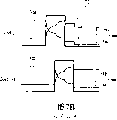
Fig. 7 A illustrates the waveform of gating signal and data voltage according to an exemplary embodiment of the present invention.Fig. 7 B illustrates according to the gating signal of prior art and the waveform of data voltage.
As shown in Figure 3, gating signal is represented to impose on pixel groups (this pixel groups composition is positioned at the same pixel row and is connected to identical data line D for Pa, Pb) j output Gout (j) and (j+1) individual output Gout (j+1)
1To D
mA pixel.In addition, data voltage represents to impose on each pixel groups (Pa, positive data voltage Pb) and negative data voltage Vda and Vdb (with "-" or "+" expression).
With reference to Fig. 7 A, the first clock signal LCLK1 and the second clock signal RCLK1 schedule time t that is separated from each other.Schedule time t can be equal to or greater than 0 and less than IH.Press phase differential, can be equal to or greater than 180 ° and less than 360 °.Example as shown in FIG., schedule time t is the 1H/2 at interval between expression first clock signal LCLK1 and the second clock signal RCLK1, that is, and 270 °.
Pixel groups (Pa, Pb) in, the data voltage that is applied with the pixel Pb of gating signal subsequently is not subjected to the influence of stray capacitance basically.It is equally applicable to Fig. 7 B.Yet the data voltage that at first is applied with the pixel Pa of gating signal increases owing to Kickback voltage or reduces.
Just, for the data voltage Vda that imposes on pixel Pa, when grid output Gout (j) when low transition is high level, at first apply pre-charge voltage, subsequently, preceding half grade of (or 1H/2) past tense as the grid of high level output Gout (j) applies target voltage.After this, carry out main charging.
Next, when grid output Gout (j) when high level is converted to low level, because the Kickback voltage that stray capacitance generated between the wiring makes pixel voltage reduce.Yet, when schedule time t in the past after next stage grid output Gout (j+1) when low transition is high level, the Kickback voltage lifting pixel voltage (voltage is just recoiling) that some P1 place generates.Similarly, the Kickback voltage that is in the generation of low level time point P2 place as next stage grid output Gout (j+1) reduces pixel voltage (negative Kickback voltage), thereby turns back to the pixel voltage before promoting.Then, shown in Fig. 7 A, positive pixel voltage Vap and negative pixel voltage Van are basic identical, thereby have prevented flicker or spot.In this case, because by considering to press Vcom, so positive pixel voltage Vap and negative pixel voltage Van become basic identical owing to the voltage that Kickback voltage caused that once takes place reduces to pre-determine common-battery.
In addition, if schedule time t is 0, that is, the negative edge of grid output Gout (j) is consistent with the rising edge of grid output Gout (j+1), and just recoiling voltage and negative Kickback voltage cancel each other out when rising and descend, so data voltage can not increase or reduce.Because negative Kickback voltage only generates at the negative edge of grid output Gout (j+1), so its result is identical with the situation with schedule time t, thereby only reduces data voltage once.
With reference to Fig. 7 B, the part of each among two gating signal Gout (j) and the Gout (j+1) all overlaps each other.Therefore, as shown in the figure, voltage is not only reducing when grid output Gout (j) descends, and also reduces when next grid output Gout (j+1) descends.Thereby, twice voltage takes place to be reduced, the voltage difference between positive pixel voltage Vap and the negative pixel voltage Van becomes much larger than the voltage difference of Fig. 7 A thus.Voltage difference between positive pixel voltage Vap and the negative pixel voltage Van may cause flicker.
Fig. 8 illustrates first to the 8th grid output Gout1 to Gout8 according to an exemplary embodiment of the present invention.
With reference to Fig. 8, second grid output Gout2 and the 3rd grid output Gout3 and the 5th grid output Gout5 are overlapping.In addition, the 4th grid output Gout4 is partly overlapping with the 5th grid output Gout5 and the 7th grid output Gout7.When data voltage being imposed on the pixel that receives the 3rd grid output Gout3, the pixel that receives second grid output Gout2 is carried out precharge.When data voltage being imposed on the pixel that receives second grid output Gout2, the pixel that receives the 5th grid output Gout5 is carried out precharge.Similarly, the 5th and the 7th grid output Gout5 and Gout7 carry out precharge in the same way.
Yet, do not have signal and first grid output Gout1 overlapping.In addition, at high-tension preceding half grade of 1H/2, there is not signal and the 3rd grid output Gout3 overlapping.Therefore, in this case, the pixel that receives grid output Gout1 and Gout3 is not carried out precharge.In order to address this problem, data voltage can be imposed on and be equal to or greater than 1H (for example, first pixel column 3H/2).By so doing, come the pixel of first pixel column is carried out precharge by apply data voltage to pixel self, and come the pixel of the 3rd pixel column is carried out precharge by apply data voltage to first pixel column.
By this way, (Pa, Pb), the pressure drop that is caused by stray capacitance only takes place once by with predetermined time-delay gating signal being imposed on pixel groups respectively.Therefore, negative pixel voltage can be identical with positive pixel voltage, thereby prevented flicker or spot.
Although described the example of exemplary embodiment of the present invention and modification, but the invention is not restricted to exemplary embodiment and example, but under the situation that does not deviate from claims, detailed description and accompanying drawing scope of the present invention, can make various forms of modifications.Therefore, very naturally, such modification within the scope of the present invention.
Claims (20)
1. driver that is used for display device comprises:
Many gate lines are used to transmit gating signal; And
First grid driver and second grid driver are connected to the gate line of the odd and even number in described many gate lines respectively, and described first grid driver and described second grid driver generate described gating signal based on a plurality of clock signals,
Wherein, two adjacent clock signals in described a plurality of clock signal have and are equal to or greater than 180 ° and less than 360 ° phase differential.
2. driver according to claim 1, wherein, two non-conterminous clock signals in described a plurality of clock signals have 180 ° phase differential.
3. driver according to claim 2, wherein, described a plurality of clock signals all have 50% dutycycle.
4. driver according to claim 1, wherein, described a plurality of clock signal comprises first clock signal to the, four clock signals, and described first clock signal and described second clock signal or described the 3rd clock signal and described the 4th clock signal have and be equal to or greater than 180 ° and less than 360 ° phase differential.
5. driver according to claim 4, wherein, described first clock signal and described the 3rd clock signal or described second clock signal and described the 4th clock signal have 180 ° phase differential.
6. driver according to claim 5, wherein, described first clock signal and described the 3rd clock signal are input to described first grid driver, and described second clock signal and described the 4th clock signal are input to described second grid driver.
7. driver according to claim 6, wherein, the first output start signal and the second output start signal are input to described first grid driver and described second grid driver respectively.
8. driver according to claim 7, wherein, described first output start signal and the described second output start signal have and are equal to or greater than 180 ° and less than 360 ° phase differential.
9. display device comprises:
A plurality of pixels are arranged;
Many gate lines are used for gating signal is transferred to described pixel;
Many data lines are used for data signal transmission to described pixel; And
First grid driver and second grid driver are connected to the gate line of the odd and even number in described many gate lines respectively, and described first grid driver and described second grid driver generate described gating signal based on a plurality of clock signals,
Wherein, two adjacent clock signals in described a plurality of clock signal have and are equal to or greater than 180 ° and less than 360 ° phase differential.
10. display device according to claim 9, wherein, two non-conterminous clock signals in described a plurality of clock signals have 180 ° phase differential.
11. display device according to claim 10, wherein, described a plurality of clock signals all have 50% dutycycle.
12. display device according to claim 9, wherein, described a plurality of clock signal comprises first clock signal to the, four clock signals, and described first clock signal and described second clock signal or described the 3rd clock signal and described the 4th clock signal have and be equal to or greater than 180 ° and less than 360 ° phase differential.
13. display device according to claim 12, wherein, described first clock signal and described the 3rd clock signal or described second clock signal and described the 4th clock signal have 180 ° phase differential.
14. display device according to claim 13, wherein, described first clock signal and described the 3rd clock signal are input to described first grid driver, and described second clock signal and described the 4th clock signal are input to described second grid driver.
15. display device according to claim 14, wherein, the first output start signal and the second output start signal are input to described first grid driver and described second grid driver respectively.
16. display device according to claim 15, wherein, described first output start signal and the described second output start signal have and are equal to or greater than 180 ° and less than 360 ° phase differential.
17. display device according to claim 16, wherein, two adjacent pixels that follow the direction setting between two adjacent data lines in described a plurality of pixels are connected to identical data line.
18. display device according to claim 17, wherein, described two adjacent pixels are connected to the gate line that differs from one another.
19. according to the display device of claim 18, also comprise the data driver that is used to generate described data-signal,
Wherein, described data driver imposes on pixel with described data-signal, and described pixel at first receives the described gating signal between described two adjacent pixels in first pixel column in a plurality of pixel columns of arranging along column direction.
20. display device according to claim 9, wherein, described first grid driver and described second grid driver are integrated in the described display device.
Applications Claiming Priority (2)
| Application Number | Priority Date | Filing Date | Title |
|---|---|---|---|
| KR1020050083039A KR101189273B1 (en) | 2005-09-07 | 2005-09-07 | Driving apparatus for display device and display device including the same |
| KR1020050083039 | 2005-09-07 |
Publications (1)
| Publication Number | Publication Date |
|---|---|
| CN1928981A true CN1928981A (en) | 2007-03-14 |
Family
ID=37829593
Family Applications (1)
| Application Number | Title | Priority Date | Filing Date |
|---|---|---|---|
| CNA2006101269326A Pending CN1928981A (en) | 2005-09-07 | 2006-09-06 | Driver for display apparatus and display apparatus including the same |
Country Status (5)
| Country | Link |
|---|---|
| US (1) | US20070052658A1 (en) |
| JP (1) | JP2007072463A (en) |
| KR (1) | KR101189273B1 (en) |
| CN (1) | CN1928981A (en) |
| TW (1) | TWI416456B (en) |
Cited By (8)
| Publication number | Priority date | Publication date | Assignee | Title |
|---|---|---|---|---|
| CN102867490A (en) * | 2011-07-05 | 2013-01-09 | 乐金显示有限公司 | Gate driving circuit |
| TWI413050B (en) * | 2009-03-17 | 2013-10-21 | Au Optronics Corp | High-reliability gate driving circuit |
| CN104570427A (en) * | 2013-10-10 | 2015-04-29 | 三星显示有限公司 | Method of driving display panel and display apparatus for performing the same |
| WO2016138734A1 (en) * | 2015-03-02 | 2016-09-09 | 京东方科技集团股份有限公司 | Shift register and drive method thereof, and gate drive circuit |
| CN109389948A (en) * | 2017-08-04 | 2019-02-26 | 乐金显示有限公司 | Gate drivers and panel display apparatus including the gate drivers |
| CN109637428A (en) * | 2019-02-18 | 2019-04-16 | 上海中航光电子有限公司 | The driving method and display device of display panel |
| CN110349534A (en) * | 2019-01-08 | 2019-10-18 | 友达光电股份有限公司 | Pixel circuit and its driving method |
| TWI688930B (en) * | 2019-02-11 | 2020-03-21 | 友達光電股份有限公司 | Electronic device and driving method thereof |
Families Citing this family (31)
| Publication number | Priority date | Publication date | Assignee | Title |
|---|---|---|---|---|
| KR101275248B1 (en) * | 2006-06-12 | 2013-06-14 | 삼성디스플레이 주식회사 | Gate driver circuit and display apparatus having the same |
| US8174478B2 (en) * | 2006-06-12 | 2012-05-08 | Samsung Electronics Co., Ltd. | Gate driving circuit and display apparatus having the same |
| TWI349909B (en) * | 2006-10-17 | 2011-10-01 | Au Optronics Corp | Driving circuit of liquid crystal display device |
| KR100891331B1 (en) * | 2007-03-13 | 2009-03-31 | 삼성전자주식회사 | Method for compensating kick-back voltage and liquid crystal display device using the same |
| JP4204630B1 (en) | 2007-05-30 | 2009-01-07 | シャープ株式会社 | Scanning signal line driving circuit, display device, and driving method thereof |
| KR101437867B1 (en) * | 2007-10-16 | 2014-09-12 | 삼성디스플레이 주식회사 | Display device, and driving device and driving method thereof |
| TWI383353B (en) * | 2007-12-27 | 2013-01-21 | Chimei Innolux Corp | Flat display and driving method thereof |
| KR101423235B1 (en) * | 2008-01-04 | 2014-07-25 | 삼성디스플레이 주식회사 | Pixel driving circuit and display apparatus having the same |
| US8547319B2 (en) * | 2008-04-30 | 2013-10-01 | Samsung Display Co., Ltd. | Display apparatus including a gate driver that has a plurality of stages and method for driving the display apparatus |
| TWI380275B (en) | 2008-07-11 | 2012-12-21 | Wintek Corp | Shift register |
| KR101502361B1 (en) * | 2008-08-06 | 2015-03-16 | 삼성디스플레이 주식회사 | Liquid crystal display |
| TWI404029B (en) * | 2008-10-08 | 2013-08-01 | Au Optronics Corp | Gate driving circuit having a low leakage current control mechanism |
| KR101478667B1 (en) * | 2008-10-16 | 2015-01-02 | 삼성디스플레이 주식회사 | Display and driving method of the same |
| KR20100083370A (en) * | 2009-01-13 | 2010-07-22 | 삼성전자주식회사 | Gate driving circuit and display device having the same |
| KR101543280B1 (en) * | 2009-02-16 | 2015-08-11 | 삼성디스플레이 주식회사 | Display panel and display apparatus having the display panel |
| TWI413040B (en) * | 2009-12-10 | 2013-10-21 | Au Optronics Corp | Pixel array |
| KR102528702B1 (en) * | 2010-02-18 | 2023-05-08 | 가부시키가이샤 한도오따이 에네루기 켄큐쇼 | Display device and electronic device |
| JP2012150215A (en) * | 2011-01-18 | 2012-08-09 | Japan Display East Co Ltd | Display device |
| KR101778650B1 (en) * | 2011-02-23 | 2017-09-15 | 삼성디스플레이 주식회사 | Display panel and display apparatus having the same |
| JP2012189752A (en) * | 2011-03-10 | 2012-10-04 | Japan Display East Co Ltd | Display device |
| WO2013179537A1 (en) | 2012-05-28 | 2013-12-05 | パナソニック液晶ディスプレイ株式会社 | Liquid crystal display device |
| KR102055152B1 (en) * | 2012-10-12 | 2019-12-12 | 엘지디스플레이 주식회사 | Display device |
| CN103021369A (en) | 2012-12-21 | 2013-04-03 | 北京京东方光电科技有限公司 | Method for driving liquid crystal display |
| KR102021579B1 (en) * | 2013-04-22 | 2019-09-17 | 삼성디스플레이 주식회사 | Liquid crystal display and driving method thereof |
| KR20160025146A (en) | 2014-08-26 | 2016-03-08 | 삼성디스플레이 주식회사 | Display apparatus |
| KR20160047653A (en) | 2014-10-22 | 2016-05-03 | 삼성디스플레이 주식회사 | Display apparatus |
| KR102281237B1 (en) * | 2015-02-13 | 2021-07-26 | 삼성디스플레이 주식회사 | Gate circuit, driving metohd for gate circuit and display device using the same |
| KR102559957B1 (en) * | 2016-09-12 | 2023-07-28 | 삼성디스플레이 주식회사 | Display Device and Driving Method Thereof |
| CN106847221A (en) * | 2017-03-20 | 2017-06-13 | 京东方科技集团股份有限公司 | Shift register cell, gate driving circuit and driving method |
| CN107230447A (en) * | 2017-08-04 | 2017-10-03 | 京东方科技集团股份有限公司 | A kind of driving method, drive circuit and display panel |
| TWI688899B (en) * | 2018-11-05 | 2020-03-21 | 友達光電股份有限公司 | Fingerprint identification module and fingerprint identification touch display using the same |
Family Cites Families (19)
| Publication number | Priority date | Publication date | Assignee | Title |
|---|---|---|---|---|
| JP2524113B2 (en) * | 1986-04-21 | 1996-08-14 | セイコーエプソン株式会社 | Liquid crystal display |
| JP2581796B2 (en) * | 1988-04-25 | 1997-02-12 | 株式会社日立製作所 | Display device and liquid crystal display device |
| JP2685638B2 (en) * | 1990-09-06 | 1997-12-03 | シャープ株式会社 | Display device |
| JPH0546123A (en) * | 1991-08-19 | 1993-02-26 | Fujitsu Ltd | Liquid crystal driving device |
| JP3132904B2 (en) * | 1992-07-09 | 2001-02-05 | 富士通株式会社 | Active matrix display |
| TW491959B (en) * | 1998-05-07 | 2002-06-21 | Fron Tec Kk | Active matrix type liquid crystal display devices, and substrate for the same |
| US6140990A (en) * | 1998-10-16 | 2000-10-31 | International Business Machines Corporation | Active matrix liquid crystal display incorporating pixel inversion with reduced drive pulse amplitudes |
| KR100312755B1 (en) * | 1999-06-03 | 2001-11-03 | 윤종용 | A liquid crystal display device and a display device for multisync and each driving apparatus thereof |
| KR100367015B1 (en) * | 2000-12-29 | 2003-01-09 | 엘지.필립스 엘시디 주식회사 | Driving Method of Liquid Crystal Display |
| JP2003101394A (en) * | 2001-05-29 | 2003-04-04 | Semiconductor Energy Lab Co Ltd | Pulse output circuit, shift register and display unit |
| US7050036B2 (en) * | 2001-12-12 | 2006-05-23 | Lg.Philips Lcd Co., Ltd. | Shift register with a built in level shifter |
| JP2003255903A (en) * | 2002-02-28 | 2003-09-10 | Toshiba Corp | Display |
| KR100487439B1 (en) * | 2002-12-31 | 2005-05-03 | 엘지.필립스 엘시디 주식회사 | Circuit and method for bi-directional driving plat display device |
| JP3904524B2 (en) * | 2003-03-20 | 2007-04-11 | シャープ株式会社 | Liquid crystal display device and driving method thereof |
| US7369111B2 (en) * | 2003-04-29 | 2008-05-06 | Samsung Electronics Co., Ltd. | Gate driving circuit and display apparatus having the same |
| US7397455B2 (en) * | 2003-06-06 | 2008-07-08 | Samsung Electronics Co., Ltd. | Liquid crystal display backplane layouts and addressing for non-standard subpixel arrangements |
| KR100945581B1 (en) * | 2003-06-23 | 2010-03-08 | 삼성전자주식회사 | Liquid crystal display and driving method thereof |
| KR20060010223A (en) * | 2004-07-27 | 2006-02-02 | 삼성전자주식회사 | Array substrate and display device having the same and a driving apparatus thereof and method driving thereof |
| US7586476B2 (en) * | 2005-06-15 | 2009-09-08 | Lg. Display Co., Ltd. | Apparatus and method for driving liquid crystal display device |
-
2005
- 2005-09-07 KR KR1020050083039A patent/KR101189273B1/en active IP Right Grant
-
2006
- 2006-09-06 JP JP2006241289A patent/JP2007072463A/en active Pending
- 2006-09-06 CN CNA2006101269326A patent/CN1928981A/en active Pending
- 2006-09-07 US US11/516,836 patent/US20070052658A1/en not_active Abandoned
- 2006-09-07 TW TW095133099A patent/TWI416456B/en not_active IP Right Cessation
Cited By (12)
| Publication number | Priority date | Publication date | Assignee | Title |
|---|---|---|---|---|
| TWI413050B (en) * | 2009-03-17 | 2013-10-21 | Au Optronics Corp | High-reliability gate driving circuit |
| CN102867490A (en) * | 2011-07-05 | 2013-01-09 | 乐金显示有限公司 | Gate driving circuit |
| CN104570427A (en) * | 2013-10-10 | 2015-04-29 | 三星显示有限公司 | Method of driving display panel and display apparatus for performing the same |
| US10417984B2 (en) | 2013-10-10 | 2019-09-17 | Samsung Display Co., Ltd. | Method of driving odd and even gate lines of a display panel, and display apparatus for performing the same |
| CN104570427B (en) * | 2013-10-10 | 2019-12-03 | 三星显示有限公司 | It drives the method for display panel and executes the display device of this method |
| WO2016138734A1 (en) * | 2015-03-02 | 2016-09-09 | 京东方科技集团股份有限公司 | Shift register and drive method thereof, and gate drive circuit |
| US9799262B2 (en) | 2015-03-02 | 2017-10-24 | Boe Technology Group Co., Ltd. | Shift register and driving method thereof, gate driving circuit |
| CN109389948A (en) * | 2017-08-04 | 2019-02-26 | 乐金显示有限公司 | Gate drivers and panel display apparatus including the gate drivers |
| CN109389948B (en) * | 2017-08-04 | 2021-07-27 | 乐金显示有限公司 | Gate driver and flat panel display device including the same |
| CN110349534A (en) * | 2019-01-08 | 2019-10-18 | 友达光电股份有限公司 | Pixel circuit and its driving method |
| TWI688930B (en) * | 2019-02-11 | 2020-03-21 | 友達光電股份有限公司 | Electronic device and driving method thereof |
| CN109637428A (en) * | 2019-02-18 | 2019-04-16 | 上海中航光电子有限公司 | The driving method and display device of display panel |
Also Published As
| Publication number | Publication date |
|---|---|
| US20070052658A1 (en) | 2007-03-08 |
| JP2007072463A (en) | 2007-03-22 |
| KR20070028744A (en) | 2007-03-13 |
| TWI416456B (en) | 2013-11-21 |
| TW200727232A (en) | 2007-07-16 |
| KR101189273B1 (en) | 2012-10-09 |
Similar Documents
| Publication | Publication Date | Title |
|---|---|---|
| CN1928981A (en) | Driver for display apparatus and display apparatus including the same | |
| CN1941063A (en) | Shift register and display device having same | |
| KR101143004B1 (en) | Shift register and display device including shifter register | |
| CN1310202C (en) | Indicator and its drive method | |
| US7728810B2 (en) | Display device and method for driving the same | |
| CN1808250A (en) | Thin film transistor array panel and display device | |
| US7956855B2 (en) | Display device using enhanced gate driver | |
| TWI413956B (en) | Display device | |
| US9082362B2 (en) | Display panel and display apparatus having the same | |
| US20120293467A1 (en) | Gate driving circuit and display apparatus having the same | |
| CN1734547A (en) | Display device with reduced interference between pixels | |
| CN1749835A (en) | Lcd | |
| US8970572B2 (en) | Display device and driving method thereof | |
| CN1790470A (en) | Display device and driving method thereof | |
| US9978322B2 (en) | Display apparatus | |
| CN1782837A (en) | Touch sensible display device | |
| CN1885379A (en) | Shift register for display device and display device comprising shift register | |
| US10621944B2 (en) | Gate voltage generation circuit, transistor substrate and display device | |
| CN1949326A (en) | Display device and testing method for display device | |
| CN1725287A (en) | Shift register, have its display device and drive its method | |
| CN1369871A (en) | Shift register and liquid crystal display using same | |
| US11908428B2 (en) | Display apparatus | |
| US20180033383A1 (en) | Display device | |
| US20150187247A1 (en) | Display panel and gate driver with reduced power consumption | |
| CN1828715A (en) | Drive circuit chip and display device |
Legal Events
| Date | Code | Title | Description |
|---|---|---|---|
| C06 | Publication | ||
| PB01 | Publication | ||
| C10 | Entry into substantive examination | ||
| SE01 | Entry into force of request for substantive examination | ||
| C02 | Deemed withdrawal of patent application after publication (patent law 2001) | ||
| WD01 | Invention patent application deemed withdrawn after publication |
Application publication date: 20070314 |