CN1455877A - Scintillator panel, radiation image sensor and method for producing them - Google Patents
Scintillator panel, radiation image sensor and method for producing them Download PDFInfo
- Publication number
- CN1455877A CN1455877A CN01815482.4A CN01815482A CN1455877A CN 1455877 A CN1455877 A CN 1455877A CN 01815482 A CN01815482 A CN 01815482A CN 1455877 A CN1455877 A CN 1455877A
- Authority
- CN
- China
- Prior art keywords
- scintillater
- scintillator panel
- multilayer film
- dielectric multilayer
- image sensor
- Prior art date
- Legal status (The legal status is an assumption and is not a legal conclusion. Google has not performed a legal analysis and makes no representation as to the accuracy of the status listed.)
- Granted
Links
Images


Classifications
-
- G—PHYSICS
- G01—MEASURING; TESTING
- G01T—MEASUREMENT OF NUCLEAR OR X-RADIATION
- G01T1/00—Measuring X-radiation, gamma radiation, corpuscular radiation, or cosmic radiation
- G01T1/16—Measuring radiation intensity
- G01T1/20—Measuring radiation intensity with scintillation detectors
- G01T1/2018—Scintillation-photodiode combinations
- G01T1/20183—Arrangements for preventing or correcting crosstalk, e.g. optical or electrical arrangements for correcting crosstalk
-
- G—PHYSICS
- G01—MEASURING; TESTING
- G01T—MEASUREMENT OF NUCLEAR OR X-RADIATION
- G01T1/00—Measuring X-radiation, gamma radiation, corpuscular radiation, or cosmic radiation
- G01T1/16—Measuring radiation intensity
- G01T1/20—Measuring radiation intensity with scintillation detectors
- G01T1/2018—Scintillation-photodiode combinations
- G01T1/20188—Auxiliary details, e.g. casings or cooling
- G01T1/20189—Damping or insulation against damage, e.g. caused by heat or pressure
Abstract
A scintillator panel (1) comprising a radiographic substrate (5) having a heat resistance, a dielectric multi-layer film mirror (6) as a light reflection film formed on the substrate (5), and a scintillator (10) formed on the mirror (6), for converting a radiation ray (30), incident onto the substrate (5) and passed through the mirror (6), into light and generating it. A heat-resisting feature provided to the substrate (5) enables a high-temperature deposition of the mirror (6) to thereby allow it to be formed with a high reflectance. In addition, the mirror (6) does not react with the scintillator (10) to be corroded unlike a metal film.
Description
Technical field
The present invention relates to middle scintillator panel, the radiation image sensor that uses it and their manufacture methods of using such as therapeutic medical radiography.
Background technology
Radioactive ray are transformed to electric signal, make the electric treatment of signal become possible radiation image sensor and be widely used in medical treatment and the industry.Can carry out electric treatment to the electric signal that obtains, and on display, show.As the representative of such radiation image sensor, have and used the radiation image sensor that radioactive ray is transformed to the scintillator material of light.In this radiation image sensor, made up the imaging apparatus that is used for again the light of institute's conversion being transformed to electric signal.To imaging apparatus, for example used the image sensor of MOS type etc.In medical field or nondestructive inspection (wherein, particularly use the inspection of microfocus x-ray source etc.), the illuminated line amount of limit radiation is so need promptly to use the illuminated line amount that is limited also can carry out the highly sensitive radiation image sensor of high light output.
Fig. 9 be the WO99/66345 communique (below, be called prior art 1.) in the longitudinal section of the radiation image sensor described.This radiation image sensor 4 be to by substrate 50, be formed on optical reflection film 60 on the substrate 50, be formed on the scintillator panel 8 that the scintillater 10 on the optical reflection film 60 is constituted, to form imaging apparatus 20 with the combinations of states of scintillater 10 relative configurations.Radioactive ray 30 by optical reflection film 60, are transformed to light with scintillater 10 from substrate 50 1 side incidents.The light of institute's conversion is transformed to electric signal by imaging apparatus 20 sensitization.Optical reflection film 60 has reflection by the light that scintillater 10 produces, and returns to scintillater 10 1 sides, is added to the function of the light quantity of the photographic department that is mapped to imaging apparatus 20.In optical reflection film 60, mainly used the metal film of aluminium etc.
Figure 10 be the spy open flat 5-196742 communique (below, be called prior art 2.) in the longitudinal section of the radioactive ray imaging device described.This radioactive ray imaging device 3 has substrate 51, be configured in the photodetector 21 as imaging apparatus on the substrate 51, be formed on scintillater 10 on the photodetector 21, be arranged on film 41 on the scintillater 10, be formed on optical reflection film 70 on the film 41, be formed on the moisture seal layer 42 on the optical reflection film 70.Radioactive ray 30 are from the 42 1 side incident of moisture seal layer.As the matrix of fixed support scintillater 10, use photodetector 21, optical reflection film 70 is formed on the scintillater 10 across film 41, and in this, its configuration structure and prior art 1 differ widely.Film 41 is made of organic material or inorganic material, absorbs concavo-convex on the scintillater 10, makes the reflectivity of optical reflection film 70 even.Wherein put down in writing and to have used the TiO that differs from one another by optical index
2And SiO
2Deng the dielectric multilayer film that constitutes as optical reflection film 70.
In this existing radiation image sensor, exist following problem.In prior art 1, use metal film as optical reflection film 60, but this metal film 60 usually corrode with scintillater 10 reactions.Particularly when using CsI (T1) as scintillater 10, this corrosion is significant.
In prior art 2, use the dielectric multilayer film as optical reflection film 70, but scintillater 10 is structures that one diameter stands in great numbers for many of the small column crystallizations of counting about μ m~tens of μ m, so exist small concavo-convex on the surface, be difficult on such male and fomale(M﹠F) and directly form dielectric multilayer film 70, institute is so that existence therebetween is used to make the film 41 of this concavo-convex planarization.When under having the state of high reflectance, forming dielectric multilayer film 70, be necessary a matrix that forms it is heated to and carry out evaporation about 300 ℃, but when this film 41 was organic membrane, it was very difficult to impose high temperature itself.Though also can form multilayer film, we can say to be difficult to the formed thickness of control that produce and formed dielectric multilayer film 70 these problems with painted state, thereby cause reflectivity to descend, light output descends with the temperature below 300 ℃.In addition,, also be difficult to form the tabular surface that is used on scintillater, forming multilayer film with inoranic membrane even will form film 41 with inoranic membrane, its result, upward generation is concavo-convex on the surface of dielectric multilayer film (reflecting surface), can't make it have higher reflectivity.
Summary of the invention
The existence of problem in view of the above the objective of the invention is to: a kind of excellent corrosion resistance is provided, and scintillator panel and the radiation image sensor and their manufacture method of higher light output can be arranged.
In order to solve described problem, scintillator panel of the present invention is characterized in that: comprising: the thermotolerance substrate; Be deposited in the dielectric multilayer film mirror on this thermotolerance substrate; On dielectric multilayer film mirror, form column structure, arrange pile up a plurality of, the radioactive ray of incident are transformed to light and the scintillater that radiates; At least cover the diaphragm of this scintillater; The mirror reflection of dielectric multilayer film makes it return to scintillater one side from the light of scintillater radiation.
Because dielectric multilayer film mirror is formed on the thermotolerance substrate, so needed when being formed on the scintillater, be used for making the uniform film of reflectivity etc. (absorbing the concavo-convex film on the scintillater) no longer necessary.And, because substrate has thermotolerance,, can form the high dielectric multilayer film mirror of reflectivity so can carry out evaporation under the high temperature.
And substrate is the radioactive ray transmissive substrate, and scintillater can be transformed to light to the radioactive ray by dielectric multilayer film mirror and produce.At this moment, for example radioactive ray are principal ingredient with CsI or NaI preferably.In addition, scintillater also can be made of the stimulated fluorophor.
Diaphragm is organic membrane preferably.At this moment, because need not form diaphragm, so this formation becomes than being easier to high temperature.
Dielectric multilayer film mirror is preferably TiO
2Or Ta
2O
5And SiO
2The multilayer film that alternately repeatedly is laminated repeatedly.This is because when being TiO
2Or Ta
2O
5And SiO
2The time, can not resemble the metallic reflective coating with the scintillater reaction and corrode, can obtain good reflection characteristic in very wide wavelength region may.
Between dielectric multilayer film mirror and scintillater, be preferably formed as the strip-proof layer that prevents that scintillater from peeling off from dielectric multilayer film mirror.Strip-proof layer can be a polyimide layer.
In addition, radiation image sensor of the present invention is characterised in that: have described scintillator panel; Dispose relative, and the light that is produced by scintillater is transformed to the imaging apparatus of electric signal with scintillator panel.In view of the above, realize comprising excellent corrosion resistance, and have the radiation image sensor of the scintillator panel of high reflectance, the light that is generated by this scintillator panel is carried out electric treatment, can be with demonstrations such as displays.
And, by having the cover of the light absorption that covers scintillator panel, can suppress the generation of the noise that the incident of the generation of the scattered light that the light scattering by dielectric multilayer film mirror causes and stray light causes, can realize that high S/N compares, high-resolution.This cover is polycarbonate system preferably, can carry out delustring at inside surface and handle.
And, if scintillator panel is close on the imaging apparatus, just can prevent the generation of crosstalking with stationary fixture, will be better.
The manufacture method of scintillator panel of the present invention has following each step: prepare the thermotolerance substrate; on this substrate, pile up the dielectric film of desired thickness repeatedly; formation has the dielectric multilayer film mirror of given reflection characteristic; scintillater at dielectric multilayer film mirror accumulation column structure covers scintillater with diaphragm.
And the manufacture method of radiation image sensor of the present invention also comprises: with the relative step that disposes imaging apparatus of scintillater with described step manufacturing.Can also comprise: use up the step that absorbefacient cover covers scintillator panel.
By these manufacture methods, just can make above-mentioned scintillator panel of the present invention and radiation image sensor rightly.
Description of drawings
Following brief description accompanying drawing.
Fig. 1 is the longitudinal section of the embodiment 1 of scintillator panel of the present invention.
Fig. 2 A~Fig. 2 F is the figure of manufacturing step of the scintillator panel of key diagram 1.
Fig. 3 is the longitudinal section of the embodiment 1 of expression radiation image sensor of the present invention.
Fig. 4 is the amplification view of action of the radiation image sensor of key diagram 3.
Fig. 5, Fig. 6 are the longitudinal sections of the embodiment 2 of explanation scintillator panel of the present invention.
Fig. 7, Fig. 8 are the embodiment 2 of expression radiation image sensor of the present invention, the longitudinal section of embodiment 3.
Fig. 9, Figure 10 are the longitudinal sections of existing radiation image sensor.
Embodiment
Below, with reference to accompanying drawing, describe the preferred embodiments of the present invention in detail.For easy understanding, in each accompanying drawing,, adopt identical reference numbering as far as possible, and omitted repeat specification for identical inscape.
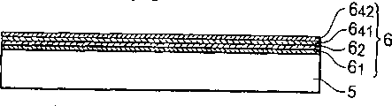
Fig. 1 is the longitudinal section of the embodiment of expression scintillator panel 1 of the present invention.Scintillator panel 1 comprises: as the Pyrex glass substrate 5 with stable on heating radioactive ray transmissive substrate; Be formed on the dielectric multilayer film mirror 6 on the Pyrex glass substrate 5; Be formed on the polyimide layer 7 on the dielectric multilayer film mirror 6 as strip-proof layer; Be formed on the polyimide layer 7, inciding on the Pyrex glass substrate 5, and be transformed to light and luminous scintillater 10 by the reflected ray 30 of dielectric multilayer film mirror 6 and polyimide layer 7.Scintillater 10 has the structure that one diameter many of small column crystallizations about for number μ m~tens of μ m stand in great numbers.Their integral body is covered by the parylene film 12 as diaphragm.Thin layer resemble SiN can be set between Pyrex glass substrate 5 and dielectric multilayer film mirror 6.This thin layer helps to make glass substrate surface to become uniform quiet surface.In dielectric multilayer film mirror 6, the TiO that has used the refractive index by light to differ from one another
2And SiO
2Alternately repeat the multilayer film that repeatedly is laminated into, as the light reflection of sending at scintillater 10, an optical reflection film that amplifies are worked.In scintillater 10, use the CsI of the T1 that for example mixed.
When formation had the scintillater of the structure that a plurality of column crystallizations stand in great numbers, the matrix of fixed support scintillater necessitated, but in the present embodiment, had used the matrix of Pyrex glass substrate 5 as the fixed support scintillater.Though, can form scintillater 10 to imaging apparatus as matrix, this moment, imaging apparatus is subjected to heat more repeatedly when forming dielectric multilayer film mirror 6 when forming scintillater 10, and the result has been subjected to infringement.In the present embodiment, because formed scintillater 10, so solved such problem for Pyrex glass substrate 5.In addition, because this Pyrex glass substrate 5 has thermotolerance, so can carry out the evaporation of nearly 300 ℃ of high temperature, in view of the above, dielectric multilayer film mirror 6 can form the high state of reflectivity.
In addition, because the excellent corrosion resistance of dielectric multilayer film, so can not corrode with scintillater 10 reactions as metal film.Corrosion when thinking metal film is by invading the moisture of scintillator panel inside, T1 among the CsI invades metal film, be necessary structure is worked hard, make moisture not enter scintillator panel inside, but in the present embodiment, because used dielectric multilayer film mirror 6, so this necessity no longer exists with strong corrosion resistant.
And, because between dielectric multilayer film mirror 6 and scintillater 10, be provided with the polyimide layer 7 as strip-proof layer, increase (particularly more than the 400 μ m) so prevented the thickness one of scintillater 10, the scintillater 10 that just might take place is peeled off from dielectric multilayer film mirror 6.
Below, described with regard to the manufacturing step of this scintillator panel 1.At first, prepare the Pyrex glass substrate 5 (with reference to Fig. 2 A) of length of side 20cm, thickness 0.5mm.On this Pyrex glass substrate 5, alternately repeat stacked TiO with vacuum vapour deposition
26
1, 6
3... 6
41With, SiO
26
2, 6
4... 6
42(with reference to Fig. 2 B, Fig. 2 C) forms by the dielectric multilayer film mirror 6 (with reference to Fig. 2 D) that adds up to 42 layers (adding up to about 4 μ m) to constitute.By controlling each thickness,, can guarantee given reflectivity to given wavelength region may as dielectric multilayer film mirror 6 integral body.
As radioactive ray transmissive substrate 5, except the Pyrex glass substrate, also can be amorphous carbon plate or aluminium sheet.When being aluminium sheet, use beaded glass (#1500) processings of sandblasting, remove the roll line on aluminium surface after, formation dielectric multilayer film mirror 6.On dielectric multilayer film mirror 6, as strip-proof layer 7, make the high polyimide layer of transparency (for example, daily output chemistry system type name RN-812) sclerosis with the rotary plating method after, apply 1 μ m (with reference to Fig. 2 E) with thickness.Then, on polyimide layer 7, form the column crystallization of CsI of thickness 300 μ m as scintillater 10 (with reference to Fig. 2 F) by vapour deposition method.Then, for the foreign matter that makes the CsI surface, the portion flattening of growing up unusually, glass plate is placed on the CsI surface, with an atmospheric power pressurization.At last, by the CVD method, the parylene film 12 that forms thickness 10 μ m covers integral body as diaphragm, forms scintillator panel 1 shown in Figure 1.
It should be noted that during large-area scintillator panel 1 more than formation has length of side 30cm, the thickness of the polyimide layer 7 of formation is 1 μ m, adopts the method for silk screen print method as coating.In addition, maximize and raising brightness in order to be accompanied by, the thickness that makes scintillater 10 is 500 μ m.
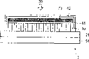
Fig. 3 is the longitudinal section of radiation image sensor 2 of the present invention.The structure of this radiation image sensor 2 is: for the scintillater 10 of scintillator panel shown in Figure 11, with the combinations of states of relative configuration imaging apparatus 20.Imaging apparatus 20 is transformed to electric signal to the light that is produced by scintillater 10.As imaging apparatus 20, for example used the image sensor of the MOS shape of Si photodiode with 2 dimension arrangements.
Fig. 4 is the amplification view of the action of this radiation image sensor 2 of explanation.Not by subject 32 shadings or the radioactive ray 30 that carried out transmission by parylene film 12, Pyrex glass substrate 5, dielectric multilayer film mirror 6, polyimide layer 7, to scintillater 10 incidents.Scintillater 10 is transformed to light to the radioactive ray 30 of incident and radiates.From the light of scintillater 10 radiation, also have towards the light of dielectric multilayer film mirror 6 one sides, this light turns back to scintillater 10 by 6 reflections of dielectric multilayer film mirror.Therefore, the light that sends is nearly all towards imaging apparatus 20, by its sensitization.Imaging apparatus 20 is the light image information conversion of sensitization to export behind the electric signal.The electric signal of like this output to transmissions such as displays, and show, but this image is that the X-ray image that incides radiation image sensor 2 is transformed to light image with scintillater 10, is transformed to electric signal at imaging apparatus 20, so be equivalent to the X-ray image of the subject 32 of incident.
As mentioned above, the dielectric multilayer film mirror 6 of present embodiment has high reflectance, so used the scintillator panel 1 of this dielectric multilayer film mirror 6 and radiation image sensor 2 to have high light output.
For the radiation image sensor 2 of estimating scintillator panel 1 sensitivity and corrosion resistance for radioactive ray 30 with such generation, change structure respectively, made as three samples (being called embodiment 1~3 respectively) of embodiments of the invention with as two samples (being called example 1,2 in the past respectively) of existing radiation image sensor.These structures of samples of table 1 expression.
The sample structure that table 1 compares

It should be noted that,, all used CsI, used parylene film, used C-MOS as imaging apparatus as diaphragm as scintillater to any one sample.
As the experiment that is used to estimate to the sensitivity of radioactive ray 30,, measured in view of the above and the light output valve that produces a certain amount of radioactive ray 30 of these sample irradiations.As the experiment that is used to estimate corrosion resistance, in each sample,, carried out the placement experiment of a few days to have removed the state of the scintillator panel monomer behind the imaging apparatus 20.Table 2 has been represented their experimental result.The light output valve is represented the relative value when example 1 is 100% in the past.
The experimental result of table 2 sample

The output valve of embodiment 1~3 is all than 1 height of example in the past that uses the aluminium film as optical reflection film, is the light output valve identical with the example in the past 2 of having used silverskin.About corrosion resistance experiment,,, in the embodiment 1~3 that has used dielectric multilayer film mirror 6, find to change through comparing of just corroding in 1st~2 with in the example in the past 1,2 of having used metal film.
In addition, in order to confirm the effect of strip-proof layer 7, carried out following experiment.As sample, at first, generate on the substrate of 10 length of side 50mm, thickness 1mm and formed 27 layers dielectric multilayer film mirror at Pyrex glass system (PX).Then,, be created on and applied polyimide layer 7 on the dielectric multilayer film mirror 6,, pile up scintillater CsI for all these samples as 5 samples of strip-proof layer and 5 samples of coating polyimide layer 7 not for each sample.CsI divides 5 phasic change thickness, and each has piled up 10.Then, the sample size that CsI peels off has taken place investigated last.
Table 3 by the thickness of CsI and whether have polyimide layer and the CsI that determines peel off generation
| CsI thickness | 100μm | ?200μm | ?300μm | ?400μm | ?500μm |
| No polyimide layer | 0/10 | ?0/10 | ?0/10 | ?3/10 | ?8/10 |
| Polyimide layer is arranged | 0/10 | ?0/10 | ?0/10 | ?0/10 | ?0/10 |
As shown in table 3, when being when not using the sample of structure of polyimide layer 7 on dielectric multilayer film mirror 6, the moment that surpasses 400 μ m at the thickness of CsI begins to peel off, and when the sample of the polyimide layer 7 that is to use, does not find peeling off of CsI.According to this experiment, confirmed that this polyimide layer 7 can prevent simultaneously when being doped with T1 scintillater 10 resembles CaI (T1) or NaI (T1), when evaporation formed scintillater, T1 was diffused in the dielectric multilayer film mirror 6 a little and painted this problem.
Like this, according to described experimental result, confirmed that the scintillator panel 1 of present embodiment and radiation image sensor 2 have higher light output, excellent corrosion resistance in addition, also has the effect that prevents that scintillater from peeling off.
Below, describe other of scintillator panel of the present invention and radiation image sensor in detail
Embodiment.
Fig. 5 is the longitudinal section of the embodiment 2 of expression scintillator panel of the present invention.This scintillator panel 1a has the structure almost same with the scintillator panel 1 of embodiment shown in Figure 11.But difference is: used stacked and had the Ta of high reflectance for the light from the visible light to the ultraviolet range
2O
5/ SiO
2Dielectric multilayer film mirror 6a; With use so-called stimulated fluorophor such as CsBr:Eu as scintillater 10a.
This scintillator panel 1a is different with scintillator panel 1 shown in Figure 1, uses radioactive ray 30 irradiations from scintillater 10a one side.By the radioactive ray of such incident, encouraged scintillater 10a.Then, as shown in Figure 6, by to scintillater 10a scanning irradiation He-Ne laser beam 34, radiate the corresponding light of dosage with the radioactive ray 30 that shine from scintillater 10a.By the light of photodetector 22 these radiation of detection,, just can take out the picture intelligence that is equivalent to X-ray image by being transformed to electric signal.
Like this, by using the stimulated fluorophor as scintillater 6a, temporarily store X-ray image, by laser beam flying it is read, thereby need not prepare large-area imaging apparatus, make the acquisition of the large-area X-ray image of fluoroscopy of chest etc. become easy.
As the stimulated fluorophor,, can also use the various fluorophor of describing in No. 3130633 communique of Jap.P. except described CsBr:Eu.In addition, as dielectric multilayer film mirror, can use the TiO that uses among the embodiment 1
2/ SiO
2Duplexer and HFO
2/ SiO
2Duplexer etc.
Fig. 7 is the longitudinal section of the embodiment 2 of expression radiation image sensor 2 of the present invention.This radiation image sensor 2a is provided with the cover 25 that covers scintillator panel 1 integral body again on radiation image sensor shown in Figure 32.Cover 25 is radioactive ray permeabilities, and protection is whole, and covers the material from the light of outside, for example the polycarbonate system of black.In view of the above, produce at scintillater 10, and the light that sees through dielectric multilayer film mirror 6 and Pyrex glass substrate 5 is absorbed by cover 25, can suppress to return the different position, luminous place with scintillater 10 1 sides again, can suppress the decline of the exploring degree that such photoconduction at random causes.In addition, also can suppress to become and come outside interference of noise light, can keep high S/N ratio.
In addition, this cover 25 is set to the state of pressure welding on the Pyrex glass substrate 5 of scintillator panel 1, by this pressure welding effect, makes scintillator panel 1 be close to imaging apparatus 20 more.In view of the above, when with imaging apparatus 20 identification by the light time that scintillater 10 produces, can prevent the generation that light leaks and crosstalks etc.In order to improve this close property, can between Pyrex glass substrate 5 and cover 25, add the elastic body of sponge etc.
As mentioned above, if as the substrate of scintillator panel 1, just having, use glass can form thin and this advantage of non-deflecting scintillator panel.In addition, if use the dielectric multilayer film, just has the advantage that can form excellent corrosion resistance and have the optical reflection film of high reflectance as optical reflection film.When the scintillator panel of this two aspect has been taked in formation, though can produce the transmitted light that becomes the reason that makes contrast decline, but in the present embodiment, by the cover 25 with light absorption also is set, just can absorb this transmitted light, make full use of the advantage of this two aspect, and problem is resolved.
Fig. 8 is the longitudinal section of the embodiment 3 of expression radiation image sensor of the present invention.In present embodiment (radiation image sensor 2b), imaging apparatus 20 is fixed on the sensor substrate 22 of having carried driving/sensing circuit, by scintillator panel 1 being fixed on the sensor substrate 22 by stationary fixture 23, be close to and be fixed on the imaging apparatus 20, covered integral body by the cover 25a of black polycarbonate system.By the synergy of stationary fixture 23 and cover 25a, scintillator panel 1 is close on the imaging apparatus 20, so when the light time that produces with imaging apparatus 20 identification scintillaters 10, can suppress the leakage of light, the generation of crosstalking etc.And in the drawings, though have the space between glass substrate 5 and cover 25, they also can be close to.According to this structure, can suppress in cover 25 internal reflections,, to cause the generation that degradation produces dysgenic light under the contrast to the output of light once again to 5 incidents of Pyrex glass substrate by behind the Pyrex glass substrate 5.
As cover 25,25a, except making cover certainly as the light absorption member, can also be that face to the inboard of contact Pyrex glass substrate 5 has carried out the member that delustring is handled, or apply the member of light absorption coating, or paste the member of light-absorbing member.
In order to estimate the contrast ratio of radiation image sensor, changed structure fabrication respectively as the sample (being called embodiment A) of the embodiment of the invention, as the sample (being called comparative example B) of existing radiation image sensor with this cover.Embodiment A and comparative example B are that structure is identical except the having or not of cover; on Pyrex glass, form dielectric multilayer film mirror; dispose the scintillater that constitutes by CsI thereon; parylene film as diaphragm; the imaging apparatus that uses the C-MOS type is as imaging apparatus, and these aspects are identical.
As the experiment that is used to measure the contrast ratio, the lead system subject of configuration diameter 3cm, thickness 0.5mm carries out radiation exposure on cover, for the hidden part of lead be presented on part in the radioactive ray, measure the signal value that radiation image sensor obtains respectively, calculate as ratio.As a result, B compares with comparative example, and in embodiment A, contrast has improved 10%, can obtain more clearly as.
Like this, according to described experimental result, confirmed that the radiation image sensor of present embodiment can obtain to have the picture of clear contrast.
From above to explanation that the present invention did as can be known, the present invention can have various distortion.And such distortion does not break away from design of the present invention and scope, and all changes apparent to those skilled in the art all should be included within protection scope of the present invention.
Scintillator panel of the present invention, radiation image sensor can be applicable to the industrial uses such as the medical applications such as fluoroscopy of chest or nondestructive inspection.
Claims (16)
1. scintillator panel is characterized in that: comprising:
The thermotolerance substrate;
Be deposited in the dielectric multilayer film mirror on the described thermotolerance substrate;
On described dielectric multilayer film mirror with column structure arrange to pile up a plurality of, the radioactive ray of incident are transformed to the scintillater that light radiates;
At least cover the diaphragm of described scintillater;
The mirror reflection of described dielectric multilayer film makes it return to described scintillater one side by the light of described scintillater radiation.
2. scintillator panel is characterized in that: comprising:
Has stable on heating radioactive ray transmissive substrate;
Be formed on the dielectric multilayer film mirror on the described radioactive ray transmissive substrate;
On described dielectric multilayer film mirror with column structure arrange to pile up a plurality of, described radioactive ray transmissive substrate of incident and the radioactive ray by described dielectric multilayer film mirror are transformed to the scintillater that light radiates;
At least cover the diaphragm of described scintillater;
The mirror reflection of described dielectric multilayer film makes it return to described scintillater one side from the light of described scintillater radiation.
3. scintillator panel according to claim 1 and 2 is characterized in that:
Described scintillater CsI or NaI as principal ingredient.
4. scintillator panel according to claim 1 is characterized in that:
Described scintillater is made of the stimulated fluorophor.
5. according to any described scintillator panel in the claim 1~4, it is characterized in that:
Described diaphragm is an organic membrane.
6. according to any described scintillator panel in the claim 1~5, it is characterized in that:
Described dielectric multilayer film mirror is TiO
2Or Ta
2O
5And SiO
2The multilayer film that alternately repeatedly is laminated repeatedly.
7. according to any described scintillator panel in the claim 1~6, it is characterized in that:
Between described dielectric multilayer film mirror and described scintillater, also has the strip-proof layer that prevents that described scintillater from peeling off from described dielectric multilayer film mirror.
8. scintillator panel according to claim 7 is characterized in that:
Described strip-proof layer is a polyimide layer.
9. radiation image sensor is characterized in that: comprising:
Any described scintillator panel in the claim 1~8;
Dispose relative with described scintillator panel is transformed to the light from the radiation of described scintillater the imaging apparatus of electric signal.
10. radiation image sensor according to claim 9 is characterized in that:
The cover that also comprises the light absorption that hides described scintillator panel.
11. radiation image sensor according to claim 10 is characterized in that:
Described cover is a polycarbonate system.
12., it is characterized in that according to claim 10 or 11 described radiation image sensors:
Inside surface to described cover has carried out the delustring processing.
13., it is characterized in that according to any described radiation image sensor in the claim 10~12:
Also comprise described scintillator panel is close to the stationary fixture that is fixed on the described imaging apparatus.
14. the manufacture method of a scintillator panel is characterized in that: comprise following each step: prepare the thermotolerance substrate;
On described substrate, pile up the dielectric film of desired thickness repeatedly, form dielectric multilayer film mirror with given reflection characteristic;
On described dielectric multilayer film mirror, pile up the scintillater of column structure;
Cover described scintillater with diaphragm.
15. the manufacture method of a radiation image sensor is characterized in that:
After the described step of claim 14, also comprise: relative with scintillater and the configuration imaging apparatus step.
16. the manufacture method of a radiation image sensor is characterized in that:
After the described step of claim 15, also comprise: use up the step that absorbefacient cover covers scintillator panel.
Applications Claiming Priority (6)
| Application Number | Priority Date | Filing Date | Title |
|---|---|---|---|
| JP275062/2000 | 2000-09-11 | ||
| JP275077/00 | 2000-09-11 | ||
| JP2000275077 | 2000-09-11 | ||
| JP275077/2000 | 2000-09-11 | ||
| JP275062/00 | 2000-09-11 | ||
| JP2000275062 | 2000-09-11 |
Publications (2)
| Publication Number | Publication Date |
|---|---|
| CN1455877A true CN1455877A (en) | 2003-11-12 |
| CN1304853C CN1304853C (en) | 2007-03-14 |
Family
ID=26599660
Family Applications (1)
| Application Number | Title | Priority Date | Filing Date |
|---|---|---|---|
| CNB018154824A Expired - Fee Related CN1304853C (en) | 2000-09-11 | 2001-09-11 | Scintillator panel, radiation image sensor and method for producing them |
Country Status (6)
| Country | Link |
|---|---|
| US (1) | US7087908B2 (en) |
| EP (3) | EP1879050A3 (en) |
| JP (2) | JP4731791B2 (en) |
| CN (1) | CN1304853C (en) |
| AU (1) | AU2001284524A1 (en) |
| WO (1) | WO2002023219A1 (en) |
Cited By (6)
| Publication number | Priority date | Publication date | Assignee | Title |
|---|---|---|---|---|
| CN101419289B (en) * | 2007-10-23 | 2012-01-18 | 浜松光子学株式会社 | Radiation image converting panel and radiation image sensor |
| CN102565839A (en) * | 2010-11-02 | 2012-07-11 | 索尼公司 | Radiation detecting element, method of producing same, radiation detecting module, and radiation image diagnostic apparatus |
| CN102819032A (en) * | 2007-06-15 | 2012-12-12 | 浜松光子学株式会社 | Radiation image conversion panel, scintillator panel, and radiation image sensor |
| CN104903745A (en) * | 2013-01-08 | 2015-09-09 | 斯基恩特-X公司 | X-ray scintillator containing a multi-layered coating |
| US10067242B2 (en) | 2015-08-06 | 2018-09-04 | Canon Kabushiki Kaisha | Scintillator, method of manufacturing the same, radiation imaging apparatus, and radiation imaging system |
| CN109874346A (en) * | 2015-12-25 | 2019-06-11 | 株式会社东芝 | Ceramic scintillators array, X-ray detector and X ray checking device |
Families Citing this family (21)
| Publication number | Priority date | Publication date | Assignee | Title |
|---|---|---|---|---|
| WO2002061459A1 (en) * | 2001-01-30 | 2002-08-08 | Hamamatsu Photonics K.K. | Scintillator panel and radiation image sensor |
| AU2001284525A1 (en) * | 2000-09-11 | 2002-03-26 | Hamamatsu Photonics K.K. | Scintillator panel, radiation image sensor and methods of producing them |
| FR2831671B1 (en) * | 2001-10-26 | 2004-05-28 | Trixell Sas | SOLID STATE X-RAY DETECTOR |
| US20040051441A1 (en) * | 2002-07-09 | 2004-03-18 | Paul Leblans | Binderless storage phosphor screen comprising a support including an amorphous (a-C) carbon layer |
| US20040026632A1 (en) * | 2002-08-02 | 2004-02-12 | Luc Struye | Stimulable phosphor screen showing less scattering upon stimulation |
| US7355184B2 (en) * | 2003-04-07 | 2008-04-08 | Canon Kabushiki Kaisha | Radiation detecting apparatus and method for manufacturing the same |
| US20040262535A1 (en) * | 2003-06-27 | 2004-12-30 | Paul Leblans | Binderless storage phosphor screen comprising a support including an amorphous (a-C) carbon layer |
| DE102006038969B4 (en) * | 2006-08-21 | 2013-02-28 | Siemens Aktiengesellschaft | X-ray converter element and method for its production |
| JP2008185568A (en) * | 2007-01-31 | 2008-08-14 | Fujifilm Corp | Radiological image conversion panel |
| JP2008209195A (en) * | 2007-02-26 | 2008-09-11 | Konica Minolta Medical & Graphic Inc | Scintillator panel and flat panel radiation detector |
| JPWO2008108186A1 (en) * | 2007-03-08 | 2010-06-10 | コニカミノルタエムジー株式会社 | Radiation imaging equipment |
| WO2008111379A1 (en) * | 2007-03-13 | 2008-09-18 | Konica Minolta Medical & Graphic, Inc. | Scintillator panel and radiation flat panel detector |
| EP3062127B1 (en) | 2007-06-15 | 2018-02-07 | Hamamatsu Photonics K.K. | Radiation image converting panel and radiation image sensor |
| US7465932B1 (en) * | 2007-06-15 | 2008-12-16 | Hamamatsu Photonics K.K. | Radiation image conversion panel, scintillator panel, and radiation image sensor |
| JP2009025075A (en) * | 2007-07-18 | 2009-02-05 | Konica Minolta Medical & Graphic Inc | Radiation scintillator panel and flat panel detector |
| CN101900824B (en) * | 2010-06-24 | 2012-05-09 | 江苏康众数字医疗设备有限公司 | Scintillator packaging thin film and packaging method thereof |
| JP2012163396A (en) * | 2011-02-04 | 2012-08-30 | Toshiba Corp | Scintillator panel and radiation detector |
| CN102496400B (en) * | 2011-12-27 | 2014-09-17 | 同济大学 | Preparation method of CsI(T1) X-ray scintillation conversion screen with microcolumn structure and application thereof |
| CN103123923B (en) * | 2013-01-31 | 2016-08-03 | 中国科学院苏州纳米技术与纳米仿生研究所 | A kind of laser photovoltaic cell and preparation method thereof |
| JP6487263B2 (en) * | 2015-04-20 | 2019-03-20 | 浜松ホトニクス株式会社 | Radiation detector and manufacturing method thereof |
| CN111123344A (en) * | 2019-12-25 | 2020-05-08 | 上海大学 | Scintillator array with multilayer reflection film and preparation method and application thereof |
Family Cites Families (34)
| Publication number | Priority date | Publication date | Assignee | Title |
|---|---|---|---|---|
| JPS59500583A (en) * | 1982-04-18 | 1984-04-05 | コスロウ テクノロジ−ズ コ−ポレイシヨン | Large-scale array of discrete ionizing radiation detectors multiplexed using fluorescent optical converters |
| FR2530367A1 (en) * | 1982-07-13 | 1984-01-20 | Thomson Csf | SCINTILLATOR SCREEN RADIATION CONVERTER AND METHOD FOR MANUFACTURING SUCH SCREEN |
| JPH0727078B2 (en) * | 1984-12-17 | 1995-03-29 | コニカ株式会社 | Radiation image information reader |
| JPS62115390A (en) * | 1985-11-14 | 1987-05-27 | Hitachi Medical Corp | Radiant ray detector |
| US4720426A (en) * | 1986-06-30 | 1988-01-19 | General Electric Company | Reflective coating for solid-state scintillator bar |
| NL8602021A (en) * | 1986-08-07 | 1988-03-01 | Optische Ind De Oude Delft Nv | METHOD FOR MANUFACTURING AN IMAGE RECORDING DEVICE FOR RADIOGRAPHIC APPLICATIONS |
| JPH01269083A (en) * | 1988-04-21 | 1989-10-26 | Hitachi Ltd | Radiant ray detecting element |
| US4947046A (en) * | 1988-05-27 | 1990-08-07 | Konica Corporation | Method for preparation of radiographic image conversion panel and radiographic image conversion panel thereby |
| FR2647955B1 (en) * | 1989-05-30 | 1991-08-16 | Thomson Tubes Electroniques | RADIOLOGICAL IMAGE ENHANCER TUBE ENTRY SCREEN |
| US5029247A (en) * | 1989-06-20 | 1991-07-02 | Kabushiki Kaisha Toshiba | X-ray image intensifier and method of manufacturing input screen |
| US5864146A (en) * | 1996-11-13 | 1999-01-26 | University Of Massachusetts Medical Center | System for quantitative radiographic imaging |
| JP3015403B2 (en) * | 1990-03-28 | 2000-03-06 | 株式会社東芝 | Method for manufacturing input surface of X-ray image tube |
| US5187369A (en) * | 1990-10-01 | 1993-02-16 | General Electric Company | High sensitivity, high resolution, solid state x-ray imaging device with barrier layer |
| US5179284A (en) | 1991-08-21 | 1993-01-12 | General Electric Company | Solid state radiation imager having a reflective and protective coating |
| US5132539A (en) * | 1991-08-29 | 1992-07-21 | General Electric Company | Planar X-ray imager having a moisture-resistant sealing structure |
| US5208460A (en) * | 1991-09-23 | 1993-05-04 | General Electric Company | Photodetector scintillator radiation imager having high efficiency light collection |
| JP3130633B2 (en) | 1992-03-05 | 2001-01-31 | コニカ株式会社 | Manufacturing method of radiation image conversion panel |
| US5463225A (en) * | 1992-06-01 | 1995-10-31 | General Electric Company | Solid state radiation imager with high integrity barrier layer and method of fabricating |
| JP3398406B2 (en) * | 1993-01-29 | 2003-04-21 | コニカ株式会社 | Radiation image conversion panel |
| JPH10160898A (en) * | 1996-11-29 | 1998-06-19 | Sony Corp | Fluorescence element and radiation image observation device |
| EP0903590B1 (en) * | 1997-02-14 | 2002-01-02 | Hamamatsu Photonics K.K. | Radiation detection device and method of producing the same |
| AU5878798A (en) * | 1997-02-14 | 1998-09-08 | Hamamatsu Photonics K.K. | Radiation detection device and method of producing the same |
| US6040962A (en) * | 1997-05-14 | 2000-03-21 | Tdk Corporation | Magnetoresistive element with conductive films and magnetic domain films overlapping a central active area |
| JP4444380B2 (en) * | 1997-09-25 | 2010-03-31 | キヤノン株式会社 | Manufacturing method of radiation detection apparatus |
| JP3334581B2 (en) | 1997-11-27 | 2002-10-15 | 松下電器産業株式会社 | X-ray image detector |
| US6031234A (en) * | 1997-12-08 | 2000-02-29 | General Electric Company | High resolution radiation imager |
| DE69901871T2 (en) * | 1998-06-18 | 2002-11-14 | Hamamatsu Photonics Kk | SCINTILLATOR PANEL AND RADIATION IMAGE SENSOR |
| EP1139120B1 (en) * | 1998-06-18 | 2005-09-28 | Hamamatsu Photonics K.K. | Radiation image sensor, and method for manufacturing the same |
| EP1118878B1 (en) | 1998-06-18 | 2005-08-17 | Hamamatsu Photonics K.K. | Scintillator panel, radiation image sensor, and method for producing the same |
| CN1260580C (en) * | 1998-06-18 | 2006-06-21 | 浜松光子学株式会社 | Scintillator panel |
| JP2000131444A (en) * | 1998-10-28 | 2000-05-12 | Canon Inc | Device and system for detecting radiation and manufacture of device therefor |
| CN100587519C (en) * | 1999-04-16 | 2010-02-03 | 浜松光子学株式会社 | Scintillator panel and radiation image sensor |
| JP2001074845A (en) * | 1999-09-03 | 2001-03-23 | Canon Inc | Semiconductor device and radiation imaging system using the device |
| JP2002148342A (en) * | 2000-11-07 | 2002-05-22 | Canon Inc | Radiation imaging device |
-
2001
- 2001-09-11 EP EP07020450A patent/EP1879050A3/en not_active Ceased
- 2001-09-11 AU AU2001284524A patent/AU2001284524A1/en not_active Abandoned
- 2001-09-11 WO PCT/JP2001/007884 patent/WO2002023219A1/en active Application Filing
- 2001-09-11 EP EP10185911.4A patent/EP2267485B1/en not_active Expired - Lifetime
- 2001-09-11 JP JP2002527812A patent/JP4731791B2/en not_active Expired - Fee Related
- 2001-09-11 US US10/363,898 patent/US7087908B2/en not_active Expired - Lifetime
- 2001-09-11 EP EP01963590A patent/EP1326093A4/en not_active Ceased
- 2001-09-11 CN CNB018154824A patent/CN1304853C/en not_active Expired - Fee Related
-
2010
- 2010-10-05 JP JP2010225851A patent/JP4800434B2/en not_active Expired - Fee Related
Cited By (9)
| Publication number | Priority date | Publication date | Assignee | Title |
|---|---|---|---|---|
| CN102819032A (en) * | 2007-06-15 | 2012-12-12 | 浜松光子学株式会社 | Radiation image conversion panel, scintillator panel, and radiation image sensor |
| CN102819032B (en) * | 2007-06-15 | 2015-11-25 | 浜松光子学株式会社 | Radiation image the Transform panel, scintillator panel and radiation image sensor |
| CN101419289B (en) * | 2007-10-23 | 2012-01-18 | 浜松光子学株式会社 | Radiation image converting panel and radiation image sensor |
| CN102565839A (en) * | 2010-11-02 | 2012-07-11 | 索尼公司 | Radiation detecting element, method of producing same, radiation detecting module, and radiation image diagnostic apparatus |
| CN104903745A (en) * | 2013-01-08 | 2015-09-09 | 斯基恩特-X公司 | X-ray scintillator containing a multi-layered coating |
| CN104903745B (en) * | 2013-01-08 | 2018-07-24 | 斯基恩特-X公司 | Include the X-ray scintillation body of laminated coating |
| US10067242B2 (en) | 2015-08-06 | 2018-09-04 | Canon Kabushiki Kaisha | Scintillator, method of manufacturing the same, radiation imaging apparatus, and radiation imaging system |
| CN109874346A (en) * | 2015-12-25 | 2019-06-11 | 株式会社东芝 | Ceramic scintillators array, X-ray detector and X ray checking device |
| CN109874346B (en) * | 2015-12-25 | 2023-04-28 | 株式会社东芝 | Ceramic scintillator array, X-ray detector, and X-ray inspection device |
Also Published As
| Publication number | Publication date |
|---|---|
| EP1326093A1 (en) | 2003-07-09 |
| CN1304853C (en) | 2007-03-14 |
| EP1879050A2 (en) | 2008-01-16 |
| JP2011002472A (en) | 2011-01-06 |
| EP2267485B1 (en) | 2013-05-15 |
| JP4731791B2 (en) | 2011-07-27 |
| JPWO2002023219A1 (en) | 2004-03-18 |
| WO2002023219A1 (en) | 2002-03-21 |
| EP2267485A1 (en) | 2010-12-29 |
| EP1879050A3 (en) | 2008-03-26 |
| US7087908B2 (en) | 2006-08-08 |
| AU2001284524A1 (en) | 2002-03-26 |
| JP4800434B2 (en) | 2011-10-26 |
| EP1326093A4 (en) | 2006-11-15 |
| US20040000644A1 (en) | 2004-01-01 |
Similar Documents
| Publication | Publication Date | Title |
|---|---|---|
| CN1304853C (en) | Scintillator panel, radiation image sensor and method for producing them | |
| JP4197593B2 (en) | Radiation image sensor and scintillator panel | |
| USRE42281E1 (en) | Scintillator panel, radiation image sensor and methods of producing them | |
| CN1265209C (en) | Flash panel and radiographic image sensor | |
| CN1207575C (en) | Radiographic detection device and system, and scintillator panel thereof | |
| US20050089142A1 (en) | Scintillator coatings having barrier protection, light transmission, and light reflection properties | |
| US7675039B2 (en) | Phosphor sheet for radiation detector, radiation detector and apparatus for radiographic equipment | |
| EP3004930A1 (en) | A moisture protection structure for a device and a fabrication method thereof | |
| JP5317675B2 (en) | Radiation detector and manufacturing method thereof | |
| JP7029217B2 (en) | Radiation detector | |
| CN103778988A (en) | Scintillator panel in indirect mode and method of manufacturing the same | |
| CN102520435A (en) | Scintillator composite board | |
| KR20150046624A (en) | X-ray detector | |
| JP2012220400A (en) | Scintillator panel, method for manufacturing scintillator panel, and radiation detector | |
| JP2003287571A (en) | Scintillator panel and its manufacturing method | |
| JP2006153707A (en) | Radiation-detecting device | |
| JPH05107362A (en) | Manufacture of x-ray detecting element | |
| JP2005181121A (en) | X-ray area sensor | |
| JP2008082764A (en) | X-ray line sensor |
Legal Events
| Date | Code | Title | Description |
|---|---|---|---|
| C06 | Publication | ||
| PB01 | Publication | ||
| C14 | Grant of patent or utility model | ||
| GR01 | Patent grant | ||
| CF01 | Termination of patent right due to non-payment of annual fee |
Granted publication date: 20070314 Termination date: 20190911 |
|
| CF01 | Termination of patent right due to non-payment of annual fee |