CN1307792C - Transmitter architectures for communications systems - Google Patents
Transmitter architectures for communications systems Download PDFInfo
- Publication number
- CN1307792C CN1307792C CNB018081258A CN01808125A CN1307792C CN 1307792 C CN1307792 C CN 1307792C CN B018081258 A CNB018081258 A CN B018081258A CN 01808125 A CN01808125 A CN 01808125A CN 1307792 C CN1307792 C CN 1307792C
- Authority
- CN
- China
- Prior art keywords
- gain
- control signal
- driver
- power
- signal
- Prior art date
- Legal status (The legal status is an assumption and is not a legal conclusion. Google has not performed a legal analysis and makes no representation as to the accuracy of the status listed.)
- Expired - Fee Related
Links
Images


Classifications
-
- H—ELECTRICITY
- H04—ELECTRIC COMMUNICATION TECHNIQUE
- H04B—TRANSMISSION
- H04B1/00—Details of transmission systems, not covered by a single one of groups H04B3/00 - H04B13/00; Details of transmission systems not characterised by the medium used for transmission
- H04B1/02—Transmitters
- H04B1/04—Circuits
-
- H—ELECTRICITY
- H03—ELECTRONIC CIRCUITRY
- H03G—CONTROL OF AMPLIFICATION
- H03G3/00—Gain control in amplifiers or frequency changers without distortion of the input signal
- H03G3/20—Automatic control
- H03G3/30—Automatic control in amplifiers having semiconductor devices
- H03G3/3036—Automatic control in amplifiers having semiconductor devices in high-frequency amplifiers or in frequency-changers
- H03G3/3042—Automatic control in amplifiers having semiconductor devices in high-frequency amplifiers or in frequency-changers in modulators, frequency-changers, transmitters or power amplifiers
-
- H—ELECTRICITY
- H03—ELECTRONIC CIRCUITRY
- H03G—CONTROL OF AMPLIFICATION
- H03G1/00—Details of arrangements for controlling amplification
- H03G1/0005—Circuits characterised by the type of controlling devices operated by a controlling current or voltage signal
- H03G1/0088—Circuits characterised by the type of controlling devices operated by a controlling current or voltage signal using discontinuously variable devices, e.g. switch-operated
-
- H—ELECTRICITY
- H03—ELECTRONIC CIRCUITRY
- H03F—AMPLIFIERS
- H03F2203/00—Indexing scheme relating to amplifiers with only discharge tubes or only semiconductor devices as amplifying elements covered by H03F3/00
- H03F2203/72—Indexing scheme relating to gated amplifiers, i.e. amplifiers which are rendered operative or inoperative by means of a control signal
- H03F2203/7239—Indexing scheme relating to gated amplifiers, i.e. amplifiers which are rendered operative or inoperative by means of a control signal the gated amplifier being switched on or off by putting into parallel or not, by choosing between amplifiers and shunting lines by one or more switch(es)
Abstract
Transmitter architectures for a communications system having improved performance over conventional transmitter architectures. The improvements include a combination of the following: faster response time for the control signals, improved linearity, reduced interference, reduced power consumption, lower circuit complexity, and lower costs. For a cellular application, these improvements can lead to increased system capacity, smaller telephone size, increased talk and standby times, and greater acceptance of the product. Circuitry is provided to speed up the response time of a control signal. The control loop for various elements in the transmit signal path are integrated. A gain control mechanism allows for accurate adjustment of the output transmit power level. Control mechanisms are provided to power down the power amplifier, or the entire transmit signal path, when not needed. The gains of the various elements in the transmit signal path are controlled to reduce transients in the output transmit power, and to also ensure that transients are downward.
Description
Background of invention
The present invention relates to the electronic circuit in the communication system, relating in particular to provides the transmitter architecture that improves performance.
Various designs are considered to make being designed to of high-performance transmitter challenging.For many application, require high-performance to satisfy the system specification.Can high performance feature be described by the linearity of the path that transmits, wide dynamic range and other characteristic of control transmitting power.And for using such as some of cellular network communication system, because the portable essence of Cellular Networks telephone set, power consumption is an important consideration very.For many transmitter design that are integrated in the mass-produced consumer products, cost also is a major consideration.High-performance, low power consumption and low cost generally are that the design of mutual contradiction is considered.
The performance and the acceptable degree of the consumer products of influence such as Cellular Networks telephone set considered in these various designs.The example of cellular network communication system comprises code division multiple access (CDMA), time division multiple access (TDMA) and analog fm (FM) communication system.U.S. Patent number 4 at " SPREAD SPECTRUM MULTIPLE ACCESSCOMMUNICATION SYSYTEM USING SATELLITE OR TERRESTRIALREPEATERS " by name, 901,307 and the U.S. Patent number 5 of by name " SYSYTEM AND METHODFOR GENERATIING WAVEFORMS IN A CDMA CELLULAR TELEPHONESYSTEM ", 103, disclosed cdma communication system in 459, both all are transferred to assignee of the present invention, and are incorporated herein by reference.Also defined cdma communication system by " TIA/EIA/IS-95-A MobileStation-Base Station Compatibility Standard for Dual-Mode Wideband SpreadSpectrum Cellular System " and " TIA/EIA/IS-95-B Mobile Station-Base StationCompatibility Standard for Wideband Spread Spectrum Cellular System ", both are referred to herein as a reference.
In cdma communication system, the non-linear generation in the transmitter shows as intermodulation distortion and reduces systematic function.Non-linear in order to reduce, the element design in the path that transmits is become to work in their range of linearity, the result has consumed a large amount of power.Require wide dynamic range to control the output transmitting power fully.In cdma system, adjust transmitted power level with desired systematic function (being a certain error rate) is provided, to the low interference of other element and the power consumption of reduction.The low power consumption of transmitter allows to use the more small-sized battery that often changes into more small-sized telephone set.Because the portability characteristic of telephone set, more small-sizedly want very much.The low power consumption of transmitter further provides the conversation and the stand-by time that increase for the battery sizes of regulation.
Such as can be seen, provide high-performance, power consumption and cheaply transmitter architecture be very desirable.
Summary of the invention
The invention provides the operation of the transmitter of control communication system, so that the controller circuitry than the improved performance of conventional transmitter to be provided.Described improvement comprises following combination: the improved linearity, the interference of reduction, the power consumption of reduction, lower circuit complexity and lower cost during fast response time, the power output of control signal are adjusted.Use public's acceptance of the conversation of the power system capacity that these improvement will cause increasing, less telephone set size, increase and stand-by time and bigger product for Cellular Networks.
An aspect of of the present present invention provides the transmitter in the communication system that comprises variable gain element, power amplifying part and controller circuitry.Described variable gain element has the variable gain that covers a certain gain ranging.Described power amplifying part is coupled to described variable gain element and comprises some discrete gain values of setting, and one of wherein said gain setting value is the bypass value of setting.Described controller circuitry provides the control signal of described variable gain element and described power amplifying part.Upgrade the gain of described variable gain element and described power amplifying part, to reduce the linearity adjustment of exporting the transient phenomena in the transmitting power and described output transmitted power level being provided in some sense.Also, control described variable gain element and described power amplifying part to reduce power consumption for example by making one or more part outages when not required.
Another aspect of the present invention provides a kind of method and apparatus of gain of the circuit element that is used for adjusting transmitter.According to this method and apparatus, receive the gain control signal that comprises the gain setting value of circuit element.Produce too drastic pulse then corresponding to the variation in the described gain setting value.To the summation of described too drastic pulse and described gain setting value, to produce control signal through adjusting, to this signal filtering to produce control signal through filtering.Adjust the gain of described circuit element then according to described control signal through filtering.Described too drastic pulse can have the amplitude that is associated with amplitude of variation in the described gain setting value and also can have the programmable duration.
Another aspect of the present invention provides a kind of method and apparatus that is used for adjusting the signal gain of the transmitter with the 1st amplifier element and the 2nd amplifier element.Described the 1st amplifier element responds the 1st refresh clock, and described the 2nd amplifier element responds the 2nd refresh clock.The the described the 1st and the 2nd refresh clock is asynchronous.According to this method and apparatus, determined respectively the described the 1st and the 2nd amplifier element the 1st and the 2nd the gain transfer characteristic.Produce the gain compensation table according to the described the 1st and the 2nd gain transfer characteristic.During normal running, receive the described the 1st and the 1st and the 2nd gain setting value of the 2nd amplifier element respectively.According to described the 1st gain setting value, adjust described the 2nd gain setting value with a certain gain deviant.From described gain compensation table, receive linearizing gain setting value then corresponding to described the 2nd gain setting value through adjusting.Respectively with the described the 1st and linearizing gain setting value adjust the described the 1st and the 2nd amplifier element.
Another aspect of the present invention provides a kind of method and apparatus that is used for adjusting the signal gain of the transmitter with the 1st amplifier element and the 2nd amplifier element.Described the 1st amplifier element responds the 1st refresh clock, and described the 2nd amplifier element responds the 2nd refresh clock.Described the 2nd refresh clock is faster than described the 1st refresh clock, and the described the 1st and the 2nd refresh clock is asynchronous.According to this method and apparatus, be respectively the described the 1st and the 2nd amplifier element and receive the 1st and the 2nd gain setting value.Produce then and represent the described the 1st and the 1st and the 2nd gain control signal of the 2nd gain setting value respectively.The the described the 1st and the 2nd gain control signal is aimed at the described the 1st and the 2nd refresh clock respectively.Detect the variation in the gain setting value of described the 1st amplifier element.If detect the variation in the described gain setting value, described the 2nd gain control signal is just aimed at described the 1st refresh clock; And if detect no change in the described gain setting value, described the 2nd gain control signal is just aimed at described the 2nd refresh clock.Adjust the described the 1st and the gain of the 2nd amplifier element with the 1st and the 2nd gain control signal of described aligning respectively.
The method and apparatus that another aspect of the present invention provides a kind of linearity that is used to provide the output power levels of transmitter to adjust.Described transmitter comprises the element with some discrete gain settings and has the element that the continuous variable gain is provided with.According to this method and apparatus, each discrete gain value of setting is determined the gain transfer function of described transmitter.For described discrete gain setting each, produce the gain compensation table according to determined gain transfer function.Reception has the 1st gain setting value of the element of discrete gain setting.Described the 1st gain setting value identifies described discrete gain and one of is provided with.Also receive the 2nd gain setting value of element with discrete gain setting.Corresponding to discrete gain setting, from described gain compensation table, fetch gain setting value through compensation by described the 1st gain setting value sign.Have the gain of the element of discrete gain setting with described the 1st gain setting value adjustment, and use the gain that has the element of variable gain setting through the gain setting value adjustment of compensation.
Another aspect of the present invention provides a kind of method and apparatus that is used for the transient phenomena of the power output that controls transmitter during signal emission.Described transmitter comprises the 1st amplifier element with the 1st time response and the 2nd amplifier element with the 2nd time response.Described the 1st time response is faster than described the 2nd time response.According to this method and apparatus, receive the 1st and the 2nd order and adjust the described the 1st and the gain of the 2nd element respectively.By described the 1st order of cycle delay sometime.Respectively with described the 1st delayed order and the gain of described the 2nd order adjustment the described the 1st and the 2nd amplifier element.Select cycle sometime to reduce the increase of the output power levels of the transmitter that the gain adjustment owing to the described the 1st and the 2nd element causes.In one embodiment, when the increase in the gain that detects described the 1st element, postpone described the 1st order.
Another aspect of the present invention provides a kind of method and apparatus that is used for the power amplifier that controls transmitter during signal emission.According to this method and apparatus, at first determine desired output transmitted power level.If desired output transmitted power level is lower than under a certain threshold value, with regard to the described power amplifier of bypass and make it the outage.Reach warm-up time at least if desired output transmitted power level above described a certain thresholding, just powers up described power amplifier, and select then to use.Can make described power amplifier outage when not in use.Can carry out selection and bypass/outage at boundary every now and then, so that the reduction degree in the systematic function reduces to minimum corresponding to the coded identification of being launched to described power amplifier.Similarly, can make path that transmits (as emission radio frequency (RF) and intermediate frequency (IF) path) and biasing circuit outage when not in use.
When with reference to below explanation, claim and during accompanying drawing, above-mentioned and others of the present invention will become clearer.
The accompanying drawing summary
Fig. 1 shows the block diagram of embodiment of the transmitter of communication system;
Fig. 2 shows the block diagram of the embodiment of the transmitter that the advantage that is better than the transmitter among Fig. 1 is provided;
Fig. 3 illustrates the block diagram to the embodiment of the controller of the generation of the transmitter among Fig. 2 control signal;
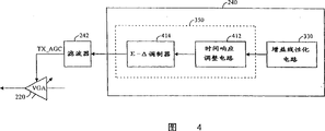
Fig. 4 shows the figure of a part of the gain controlling mechanism of the embodiment that comprises interface circuit;
Fig. 5 shows the figure of the specific embodiment of described interface circuit;
Fig. 6 shows the block diagram of the embodiment of gain compensation circuit;
Fig. 7 A is the sequential chart of the control signal of power amplifier driver (driver-PA) and variable gain amplifier (VGA);
Fig. 7 B shows the block diagram of the embodiment of the control signal that produces driver-PA and VGA;
Fig. 7 C and 7D show regularly the block diagram of the embodiment of comparator in the synchronous circuit and logical circuit respectively;
Fig. 8 A and 8B show the block diagram of the embodiment with high efficiency power amplifier (HEPA) that a plurality of gain settings and bypass be provided with and power amplification circuit respectively;
Fig. 8 C shows the figure that has a plurality of gain settings and do not have the embodiment of the power amplifier (PA) that bypass is provided with;
Fig. 9 A shows the gain transfer function curve (or curve) such as the typical circuit of VGA, driver (driver) or PA.
Fig. 9 B and 9C illustrate the power hysteresis phenomenon of the circuit element with 2 gain-state and the curve of power and timing hysteresis phenomenon respectively;
Fig. 9 D and 9E illustrate the power hysteresis phenomenon of the circuit element with 4 gain-state and the curve of power and timing hysteresis phenomenon respectively;
Figure 10 A and 10B show respectively for the step that gains downwards and upwards and change, because the curve of the transient phenomena in the output transmitting power that the mismatch in the response time of driver-PA and VGA causes;
Figure 10 C shows for two different time delays with 10D, because the curve of the transient phenomena in the output transmitting power that the mismatch of control signal in time alignment of (deliberately introducing) driver-PA and VGA causes;
Figure 10 E shows the control signal of delay driver-PA can control the block diagram of the embodiment of circuit of exporting the transient phenomena in the transmitting power when switching the gain of described driver-PA;
Figure 11 A and 11B show the sequential chart of the signal that is used to control PA and transmitting chain according to an aspect of the present invention;
Figure 11 C shows and produces the figure that control signal PA_ON makes the embodiment of circuit of described PA energising or outage;
Figure 11 D shows and produces control signal PA_R[1:0] the figure of embodiment of circuit.
The explanation of specific embodiment
Transmitter architecture
Fig. 1 shows the block diagram of embodiment of the transmitter 100 of communication system.Transmitter shown in Fig. 1 can be used for various application, comprises Cellular Networks telephone set, high-definition television (HDTV), cable TV and other.In the emission path, intermediate frequency (IF) signal is amplified by variable gain amplifier (VGA) 120, be up-converted into radio frequency (RF) by frequency mixer 122 usefulness from the sinusoidal signal of local oscillator (LO) 124, amplify by driver (driver) 126, and cushion by the power amplifier (PA) 128 of driven antenna 130.According to the desired linearity, driver126 and power amplifier 128 are by switch 132 coupling paramount power supply source (VDD_high) or the low power supply sources (VDD_low) by control signal PA_R1 control.The transmitting chain of transmitter 100 comprises the element the path that transmits (promptly from frequency mixer 122 to antenna 130), but does not support the circuit such as local oscillator 124.Described transmitting chain comprises frequency mixer 122, driver126 and PA128.
In the embodiment shown in fig. 1, when being enabled by control signal PA_ON, PA128 provides fixed gain (as 29dB), and according to the state of control signal PA_R0, driver126 provide the 1st or the 2nd gain (as be respectively 26dB or-2dB).VGA120 provides enough gain controlling with the desired dynamic range of covering system specification (as 85dB).Controller 140 produces the control signal that starts PA128, be provided with driver126 gain, control PA128 and driver126 biasing and the gain of VGA120 is set.
Require transmitter 100 to satisfy the various system specifications.Use for CDMA, require transmitter with up to the nonlinear operation of ormal weight and the dynamic range of regulation is provided.By high power supply power supply (VDD_high) being provided and, partly reducing non-linearity to driver126 and PA128 by being that diver126 selects suitable gain (as high-gain) with the high transmit power level.Though driver126 can be in one of two gain settings operation, because following former reason VGA120 provides desired dynamic range.
In transmitter architecture shown in Figure 1, by mechanism controls driver126 with a renewal rate and PA128, and by another mechanism controls VGA120 with the 2nd renewal rate.Usually, by to bypass of high power driving stage or outage, realize the low gain state of driver126.When driver126 changed gain-state, the normal gain short-time pulse waveform that takes place disturbed and undesired and uncertain phase deviation.These adverse effects have reduced the performance of system.As a result, with the gain of low rate switching driver126, to reduce adverse effect.On the contrary, the gain controlling mechanism of described VGA120 has general fast renewal rate than driver126.Described very fast renewal rate is used for promptly adjusting the gain of the path that transmits, with the rapid variation in the responsive operation condition.
In cdma communication system, the refresh clock of described power amplifier driver (driver-PA) controlling organization and the refresh clock of described VGA controlling organization are frequency locks, but can not be (and not being usually) phase locking.Can regard these refresh clocks as asynchronous in fact.Because system design as described below considers that the refresh clock of described driver-PA derives from the modulator of the unit (as subscriber unit) that transmitter is arranged therein, and the refresh clock of described VGA controlling organization derives from demodulator.
The mechanism of control driver126 and PA128 generally has the fast response time of mechanism than control VGA120.As shown in fig. 1, the control signal of driver126 and PA128 (PA_R0 and PA_R1) be in essence numeral and have (relative) fringe time faster.On the contrary, the control signal VGA_GAIN of VGA120 responds τ sometime by having
1 Low pass filter 142 filtering.The bandwidth Design of filter 142 is become narrower, as the system specification is desired, the ripple magnitude on the gain control signal TX_AGC is reduced to particular value.The response time that (relatively) that narrow bandwidth causes the step among the control signal VGA_GAIN is changed grows is (as τ
1≌ 330 microseconds).
At least some reasons because above-mentioned reason in (being different renewal rate, asynchronous refresh clock and different response times) typically are designed to described driver-PA controlling organization and described VGA controlling organization work independently of one another.Yet at the output transmitted power level that keeps approximately constant when the gain of driver126 when the low gain setting switches to high-gain and is provided with, and vice versa, and described two controlling organizations just are coupled.When between gain is provided with, switching the gain of driver126, in described transmitting chain, introduced unexpected gain step, this will cause exporting the variation in the transmitted power level.In order to compensate this gain step, with the gain of offset gain adjustment VGA120, so that the entire transmit signal path gain of approximate similarity to be provided before or after switching driver126.For example, if driver126 is switched to+the 26dB gain from-2dB gain, the gain of VGA is reduced 28dB to compensate described driver change in gain at approximate synchronization.The response time of VGA120 should critically be mated the response time of driver126.Suitably do not adjust the gain (promptly because the slower response time) of VGA120 if switched the gain of driver126, gain transients then takes place, this causes the transient phenomena of the correspondence in the output transmitting power.Described power transient phenomenon can cause the reduction of the performance of transmitter.
Fig. 1 shows synchronous described 2 controlling organizations to reduce the realization of gain transients when switching described driver.Low pass filter 142 is coupled to controller 140, and reception and filtering controlled variable signal VGA_GAIN, offers the aanalogvoltage of summing amplifier 148 with generation.Control signal PA_R0 coupling and the control switch 144 of driver126, described switch is coupled between low pass filter 146 and the summing amplifier 148.Filter 146 is coupled to controller 140, and reception and the constant control signal OS_GAIN of filtering, offers the constant aanalogvoltage of summing amplifier 148 with generation.The voltage summation that receives of 148 pairs in amplifier then is to produce VGA control signal TX_AGC.
Thereby when switching the gain of driver126, the corresponding fixed gain bucking voltage OS_GAIN of filtering (promptly through) offers VGA120.Described gain compensation voltage is adjusted the gain of VGA120 to keep the entire transmit signal path gain of approximately constant with opposite direction.The response time of amplifier 148 is insignificant, and the response time of driver126 is near the variation among the control signal PA_R0.Because with respect to the fast-response time (generally can ignore) of driver126, the response time of filter 142 (about 330 microseconds) is too slow, before filter 142, need not digital method add described gain compensation voltage (promptly in controller 140).
Owing to some reasons, the transmitter architecture shown in Fig. 1 is not best.At first, because the independent operation of the gain controlling mechanism of driver126 and VGA120, whole dynamic range requires (as 85dB) just to be applied on the VGA120.This wide dynamic range requires to cause VGA design complicated and power consumption.Secondly, the additional element that when switching driver126, needs for the output transmitted power level that keeps approximately constant (as, outside-switch 144, filter 146 and summing amplifier 148; And inner-be used for the extra PDM of the D/A conversion of signal OS_GAIN) will increase and launch hardware complexity and cost.
Transmitter architecture shown in Fig. 1 can't satisfy some system requirements.For example, the mean output power level of TIA/EIA/IS-98-A requirement transmitter will being less than within the 0.3dB that is in end value in 500 microseconds after receiving the effective power control bit.The wide bandwidth powered controls that requirement has quick settling time satisfy this regulation.Receive and the required processing time of validity of definite power control bit almost is 400 microseconds, only stayed for 100 microsecond times and respond detected effective power control bit to transmitter.If, then being difficult to (if not impossible) greater than 100 microseconds (approximately being 330 microseconds) in modular design, the response time of filter 142 satisfies this regulation.
Such as can be seen, various design considerations and system requirements require speed and accuracy to put in the gain controlling mechanism of described transmitting chain.
Fig. 2 shows the block diagram of the embodiment of the transmitter 200 that the transmitter 100 that is better than among Fig. 1 is provided.In the emission path, intermediate frequency (IF) signal is amplified by VGA220, is up-converted into radio frequency by frequency mixer 222 usefulness from the sinusoidal signal of local oscillator 224, amplify by driver226, and by the PA228 buffering of driven antenna 230.Driver226 and PA228 are coupled to PA control circuit 232, and this circuit receives the control signal PA_R0 and the PA_R1 of self-controller 240.The transmitting chain of transmitter 200 comprises VGA220, frequency mixer 222, driver226 and PA228.Also can be implemented in PA control circuit 232 among the controller 240.In specific embodiment shown in Figure 2, PA228 has that 3 gains are provided with and driver226 has 2 gains and is provided with.Described PA gain is provided with and comprises low gain, high-gain and bypass, and described driver gain setting comprises low gain and high-gain.Controller 240 produces the control signal that starts PA228, and the gain of driver226 and PA228 is set, and the biasing of control driver226 and PA228 also is provided with the gain of VGA220.CGA_GAIN offers filter 242 the VGA gain control signal, and described filter carries out filtering offers VGA200 with generation gain control signal TX_AGC to described signal.
Transmitter 200 comprises following characteristics and advantage.At first, as described below, the gain controlling mechanism of amplifier element (VGA220, driver260 and PA228) is integrated so that improved performance to be provided.Partly by providing the circuit of very fast response time to make described controlling organization integrated for described VGA gain control signal.
Secondly, dynamic range requires to be distributed in the amplifier element in the transmitting chain.Use integrated gain controlling mechanism, can use 3 of PA228 gains to be provided with potentially and 2 gain settings of driver226, so that some desired dynamic range to be provided, thereby reduced dynamic range requirement VGA220.For example, the dynamic range of the 85dB that can distribute requires (VGA120 among Fig. 1 provides), makes driver226 and PA228 that 55dB is provided dynamic range, and VGA provides the dynamic range of residue 30dB.With lower dynamic range requirement, can be designed to VGA220 that power is effective more, thereby reduce power consumption, and also can realize (this will be required in direct upconversion transmitter structure) on the RF.
Further described below based on improved extra benefit and advantage in the transmitter architecture of Fig. 2.
Fig. 3 illustrates the block diagram to the embodiment of the controller 240 of the 200 generation control signals of the transmitter among Fig. 2.In controller 240, automatic gain control (AGC) signal is provided for the loop filter 310 that this control signal is carried out filtering.Last/issuing orders offers closed power control circuit 312, this circuit produce step yield value with response received on/issue orders.Offering adder 314 and combination from the output of loop filter 310 with from the output of power control circuit 312.Then the composite signal from adder 314 is offered load limiter 316, restricting signal is to prevent the excessive emission from transmitter 200.Constrained signal from described limiter 316 is offered adder 318, and this adder also receives the gain compensation signal from gain compensation circuit 320.Adder 318 offers the gain signal of gain linearization circuit 330 with described two input signal additions with generation.Gain linearization circuit 330 produces (i.e. " the linearizing ") control signal through compensation, and this signal is amplifier element nonlinear that is used for solving transmitting chain.Described control signal through compensation is offered the interface circuit 350 that produces described control signal VGA_GAIN.PA_RANGE control circuit 360 receives the control input of the mode of operation of indication transmitter, operating characteristic and the TX_AGC value of wanting.Then, in response, the work of control circuit 360 ride gain linearizers 330 also produces control signal PA_R0, PA_R1 and PA_ON.Regularly synchronous circuit 340 is synchronous with described VGA control signal and driver-PA control signal.The operation of each element in the controller 240 has been described in further detail below.
Gain controlling mechanism with fast response time
Gain controlling mechanism with fast response time provides some advantages.At first, because fast response time arranged, can produce the control signal of VGA and the gain compensation signal of the VGA switching of the gain of described driver-PA (promptly owing to) with the method for numeral and their are made up to form the VGA gain control signal of single combination.For the transmitter architecture shown in Fig. 1, may change in the gain of described driver-PA each, will require extra PDM, extra one group of switch 144 and filter 146 and operational amplifier add circuit 148 to produce and a certain gain compensation signal that is coupled.Thereby, if described driver-PA comprises 4 possible gain settings, need 3 groups of PDM, switch and filters and operational amplifier add circuit, to produce 33 compensating signals that may change that change from the driver-PA nominal gain corresponding among the driver-PA.Described extra switch, filter and operational amplifier add circuit have increased transmitter hardware complexity.In addition, for 4 possible gain settings, current available controller 140 can not provide extra desired PDM.
According to an aspect of the present invention, the gain compensation signal of described VGA (promptly because the variation in the described driver-PA gain) produces with digital form and with the gain control signal addition of digital form and VGA, with single whole gain control signals of generation VGA.As a result of, only need the low pass filter of a PDM and an outside, to produce described VGA gain control signal.Yet as mentioned above, driver226 and PA228 can be relative very fast to the time response of the variation in its control signal.The gain compensation signal of VGA should have the time response of approximate similarity, so that the gain transients in the path that transmits is reduced to is minimum.This can have wide bandwidth by design and realize with the low pass filter 242 of the response time of response time that approximate match driver226 and PA228 are provided.In specific embodiment, filter 242 has 70% the settling time that is approximately 10 microseconds, and this makes emission function meet the IS-98A requirement.
The time constant of increase filter 242 has increased the ripple magnitude on the control signal TX_AGC.In the typical case realized, described control signal VGA_GAIN was pulse density modulated (PDM) signal that comprises high and low value sequence.There are 242 pairs of described height of filter and low value to carry out filtering to obtain the value of equalization.Analog control signal corresponding to this equalization value drives described VGA.Described height and low value produce the ripple that reduces transmitter performance in described analog control signal.In order to reduce ripple magnitude, can carry out extra filtering (promptly by reducing filter bandwidht).Though described extra filtering has reduced ripple magnitude, has relatively slowed down the response time.
Fig. 4 shows the figure of a part of the gain controlling mechanism of the embodiment that comprises interface circuit 350.Interface circuit provides improved time response and has kept (or reduction) described ripple magnitude.The control signal through compensation from gain linearization circuit 330 offered adjust time response in the interface circuit 350 circuit 412.As described in below inciting somebody to action, circuit 412 produces " through what adjust " control signal of the time response that has through adjusting.Described signal through adjusting is offered the sigma-delta modulator 414 that produces modulator signal.Described modulator signal comprises the wave sequence corresponding to the value in the described control signal through adjusting.242 pairs of described modulator signal of filter receive also filtering so that described VGA control signal TX_AGC to be provided.
Fig. 5 shows the figure of the specific embodiment of described interface circuit 350.Interface circuit 350 comprises adjusts circuit 412 and single order sigma-delta modulator 414 time response.Described control signal x[n through compensation] offer and adjust circuit 412 time response, this circuit produces the control signal y[n through adjusting].In one embodiment, described control signal through adjusting comprises the correction through the control signal of compensation to response time of providing very fast or revising.
Adjust in the circuit 412 in time response, signal x[n] offer amplifier element 520 and delay element 522.Amplifier element 520 is can be zoom factor that fix or programmable (Av) scale signal x[n].In specific embodiment, described zoom factor is 2.Delay element 522 is also can be time interval inhibit signal x[n that fix or programmable].Described zoom factor and described retardation depend on the requirement of the application-specific of using interface circuit 350 therein.From amplifier element 520 offer adder 524 through the signal of convergent-divergent with from the delayed signal of delay element 522, this adder deducts described delayed signal from described through the signal of convergent-divergent.In one embodiment, adder 524 is saturated adders, with the N bit value of its export-restriction in the input range of the sigma-delta modulator 414 that lags behind.Signal y[n from adder 524] offer sigma-delta modulator 414.
In sigma-delta modulator 414, signal y[n] offer adder 530, N minimum effective bit (LSB) the plus signal y[n of this adder] from register 532.(N+1) bit of adder 530 output offered register 532 and by its storage.The highest significant bit from register 532 comprises the modulator signal k[n through quantizing that offers filter 242].Shown in the embodiment among Fig. 5, though clock signal (SYS CLK) timing that delay element 522 is identical with register 532 usefulness is this optional condition.
The modulator signal filtering of filter 242 devices of automodulation in the future 414 is to produce analog control signal TX_AGC.In the specific embodiment shown in Fig. 5, filter 242 is the second-order low-pass filters that comprise two resistors and two capacitors.
In order to improve the response time of described control signal TX_AGC, adjusting the too drastic pulse that circuit 412 is designed to produce the response of extension filter 242 time response.For example, when 2 (Av=2) were arranged in the gain of amplifier element 520, circuit 412 produced to have and equals described signal x[n] in the too drastic pulse of amplitude of variation.According to x[n] value and x[n] in the amplitude that changes, the amplitude of described too drastic pulse can be less in some cases.Each too drastic pulse has the MT that is determined by described delay element
sDuration.
Sigma-delta modulator 414 provides modulator signal k[n], this signal comprise corresponding to its input through adjusting control signal y[n] the height and the low value sequence (being the output waveform sequence) of signal.Sigma-delta modulator 414 is at the interval that distributes equably among the output waveform between high value, to provide than conventional pulse-width modulation (PWM) and the improved stable state ripple of conventional PDM performance.This characteristic causes less ripple magnitude, has identical time quantum because the capacitor in the filter 242 charges to every group of height and low value with discharge.Analysis points out that with 9 bit resolutions (N=9) sigma-delta modulator 414 can be reduced to 1/3 or littler with the bad situation of peak-to-peak ripple amplitude.Improvement in these ripple performances can be used for exchanging for the response time faster.Especially, by increasing the bandwidth of 3 times of described low pass filters, can obtain 3 times of raisings of response time for identical ripple magnitude.
Low-pass first order filter typically is used for the modulator signal k[n from described modulator] carry out filtering.Can realize described firstorder filter with single resistor and single capacitor.Though firstorder filter causes the less elements number, use the described response time and the ripple performance is unsatisfactory for some.
For second order filter with two limits, the frequency response of filter between the frequency of the 1st and the 2nd limit with 1/f decay, and after the frequency of described the 2nd limit with 1/f
2Decay.Being lower than ripple component by the frequency of selecting two limits (is f
P1And f
P2<f
Ripple), described ripple is with 40dB/10 slope decay doubly, and this is faster than the 20dB/10 that obtains with firstorder filter slope doubly.Improvement in the ripple can exchange the raising in response time of filter for then.In other words, in order to satisfy specific ripple requirement, the limit of described second order filter can be increased to the limit height than firstorder filter, thereby causes faster the response time and do not sacrifice the ripple performance.
Described ripple performance be modulator type (as conventional PDM, sigma-delta modulator or the like), as described in the function of speed of the bandwidth of low pass filter and modulator clock.Can illustrate, the clock frequency of quickening described sigma-delta modulator causes the correspondence of ripple quantity to reduce.By increasing the bandwidth of analog filter, the improvement in the ripple performance can be used for exchanging for the response time faster then.
The realization and the operation of circuit 412, sigma-delta modulator 414 and filter 242 have been described in further detail in related application sequence number 19622-2.
The integrated gain controlling mechanism of transmitting chain
Control the circuit that VGA gains with providing fast response time to be used to, the gain controlling mechanism of driver226 and PA228 can integrate with the gain controlling mechanism of VGA220.In one implementation, with of the gain of specified mode by control signal PA_R0 and PA_R1 control driver226 and PA228.When changing driver226 or PA228 or both gains, from the VGA control signal, deduct gain compensation value corresponding to the variation in the described driver-PA gain with digital form.Then whole VGA control signal is carried out filtering and offered VGA220.
In the embodiment shown in Figure 2, driver226 comprises that 2 gains are provided with, and PA228 comprises that 3 gains are provided with.Can make up these gains is provided with to form 3 to 6 driver-PA gain settings.In specific embodiment, make up these elements and be provided with 4 gains that form by table 1 definition.
The gain-state of table 1-driver and PA
| The driver-PA gain-state | Output transmitting power scope | The driver gain is provided with | The PA setting that gains | Driver-PA gain |
| 0 | -52dBm is to-17dBm | Low gain | By bypass | 0dB |
| 1 | -32dBm is to+3dBm | High-gain | By bypass | 20dB |
| 2 | -14dBm is to+21dBm | High-gain | Low gain | 38dB |
| 3 | + 5dBm is to+28dBm | High-gain | High-gain | 56dB |
When the described driver-PA of change gains, correspondingly compensate the gain of VGA220, with the variation in the explanation driver-PA gain, with the approximately uniform transmitted power level of maintenance before and after described driver-PA change in gain.For example, when described driver-PA gain when gain-state 1 changes to gain-state 2, described driver-PA has increased about 18dB.Thereby, the gain compensation value that reduces the gain of described VGA with 18dB is added to described VGA control signal.At about synchronization of the gain that changes described driver-PA, adjust described VGA gain, make transient phenomena minimum in the described output transmitting power.
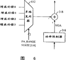
Fig. 6 shows the block diagram of the embodiment of gain compensation circuit.4 gain compensation value are offered 612, one gain compensation value of multiplexer (MUX) corresponding to each of described driver-PA gain-state.Can be stored in these gain compensation value in memory (as RAM, ROM, flash memory or other memory technology), one group of register, controller or other circuit.MUX612 also receives control signal PA_RANGE_STATE[1:0], this control signal selects one of described gain compensation value to offer adder 318.Adder 318 deducts selected gain compensation value from the VGA yield value then, so that described whole VGA yield value to be provided.
For 4 gain-state of described driver and PA, only need 3 gain compensation value (from the nominal gain value).Thereby can reduce the complexity of MUX612.Yet with the realization of 4 gain compensation value, one of them gain compensation value is corresponding to each of described driver-PA gain-state, allows in the transmitter design greater flexibility and also avoided the saturated of data path.
As top indicated go out, for cdma communication system, typically use a refresh clock to produce the control signal of driver226 and PA228, and use another refresh clock to produce the control signal of VGA220.These two clocks are typically frequency lock, and are not phase locking generally.For the transmitting gain controlling organization, because the control signal that needs described driver-PA of alignment and VGA to be to reduce the transient phenomena in the output transmitting power, phase difference comes down to problematic between described two clocks.
In complying with the cdma communication system of IS-95-A, run through the transfer of data that takes place in the transmission course of Walsh code element from the subscriber unit to the base station.In subscriber unit, produce, encoded data bits, and it is grouped into the group of every group of 6 encoded data bits.Every group of table that is used to point out a Walsh code element.Each Walsh code element is 64 bits and duration with 208 microseconds, promptly causes the Walsh chip rate of 4.8kHz.Described base station is modulated and sent it to described Walsh code element.At the place, base station, receive and separate the signal that menstruation regulating sends.Usually on each Walsh code-element period, carry out coherent demodulation, and on a plurality of Walsh code elements, carry out non-coherent demodulation.For coherent demodulation, the phase information of the signal that is received has a significant impact demodulation performance.
In specific embodiment, because the switching of the gain of described driver or described PA is easy to produce the instantaneous phase fluctuation and be interrupted in output transmits, die and the switching of described driver and PA is restricted to the border of described Walsh code element, reduce to minimum so that performance is reduced.By with the switching of the gain of described driver and PA and the boundary alignment of described Walsh code element, the transient phenomena in the output transmitting power appear at the boundary of described code element, and have reduced the reduction degree of systematic function.This design alternative causes switching described driver and PA with the Walsh chip rate of 4.8kHz.
The 4.8kHz renewal rate generally is enough the switching between gain-state, is that the typical case is not enough for the VGA gain controlling still.Generally renewal rate makes VGA can promptly adjust the output transmitted power level faster, with the rapid variation in the responsive operation condition.In realizing in detail, the renewal rate of VGA is 38.4kHz.In realizing in detail, the refresh clock of described driver-PA gain setting circuit is the 4.8kHz clock of the modulator in the radiating portion that stems from the subscriber unit, and the refresh clock of described VGA gain setting circuit is the 38.4kHz clock that stems from the demodulator in the receiving unit of subscriber unit.
For the communication system of complying with IS-95-A, on the constant time lag between received frame border and transmit frame border, applied the requirement of 10 microseconds.This postpones typically short than the processing delay of subscriber unit.Thereby, before receiving the frame that is received, carry out some processing in the transmitter in advance.Described transmitter timing and receiver timing dynamical correlation cause the asynchronous timing between transmitter and receiver.Asynchronous timing between this VGA control signal that causes stemming from the driver-PA control signal of transmitter timing and stemming from the receiver timing.
As described below, for integrated gain controlling mechanism is provided, the control signal of (promptly when described driver-PA change gain is provided with) synchronous described driver-PA and VGA as in case of necessity.
Fig. 7 A is the sequential chart of the control signal of driver-PA and VGA.The 4.8kHz refresh clock that can notice driver-PA does not align with the 38.4kHz refresh clock of VGA.At moment t
1The place, current with previous gain-state is identical (promptly all being in gain-state 00 place), and with the input of the controlling value updating interface circuit 350 of the specified mode of 38.4kHz clock.At moment t
2The place, current with previous gain-state is different (promptly changing to gain-state 01 from gain-state 00), and with the input of the controlling value updating interface circuit 350 of use 4.8kHz clock.Generation intermediate control signal SAME and ALIGN assist the VGA controlling value are snapped to suitable refresh clock.In one embodiment, if described SAME control signal is low, promptly indicate the change in the driver-PA state, then before the forward position of 4.8kHz and afterwards, described ALIGN control signal stops the renewal of interface circuit 350 to reach a 38.4kHz clock cycle.This has guaranteed that interface circuit 350 does not produce the not enough or too drastic control signal of big driving to VGA, with the variation in the response gain-state, and guarantees that described PDM filter has time enough that big gain step is carried out filtering.If described SAME control signal is high, promptly indicate no change in described driver-PA state, then with the input of normal mode updating interface circuit 350.4.8kHz clock (being marked as 4.8kHz_E) according to " in early days " version shown in the top of Fig. 7 A produces described control signal SAME and ALIGN.Be described at the control signal LOAD_EN1 shown in the bottom of Fig. 7 A the update time of the input of interface circuit 350.
Fig. 7 B shows the block diagram of the embodiment of the control signal that produces driver-PA and VGA.Described gain-state is determined (promptly according to control input and TX_AGC value) by PA_RANGE control circuit 360 and is provided for comparator 722 in the timing synchronous circuit 340.Comparator is receive clock signal SYS CLK and described 4.8kHz_E clock also, current gain-state and the last gain-state of driver-PA is compared, and produce described SAME and the ALIGN control signal that whether changes in the indication driver-PA gain-state.Described SAME and ALIGN control signal are offered logical circuit 724, and described logical circuit is written into the permission signal to gain linearization circuit 330 and interface circuit 350 generations.Be written into permission signal LOAD_EN0 and be used to latch the output (this output is the input of interface circuit 350) of gain linearization circuit 330, and be written into the delay element 522 that allows signal LOAD_EN1 to be used for enabling interface circuit 350.Described signal LOAD_EN0 and LOAD_EN1 guarantee to upgrade at synchronization/enable the input of the delay element 522 in interface circuit 350 and the interface circuit 350.Shown in Fig. 7 A, described being written into allows signal LOAD_EN1 to comprise starting impulse, and described starting impulse snaps to the 38.4kHz clock in normal work period, and when changing in the driver-PA gain-state, it snaps to the 4.8kHz clock.System clock SYS CLK (or the clock with similar phase place) latchs the outputting VGA _ GAIN of interface circuit 350 and output PA_R0, PA_R1 and the PA_ON of control circuit 360, with the phase alignment with these control signals.
Fig. 7 C shows the block diagram of the embodiment of comparator 722.In comparator 722, the PA_RANGE_STATE signal is offered the data input of register 732 and the A input of comparator 734 and 736.To register 732 timing, and enable register 732 with clock signal SYS CLK, and the output of register 732 is offered the B input of comparator 734 and 736 with described 4.8kHz_E clock.Register 732 keeps the last gain-state value of driver-PA.Comparator 734 and 736 each comparison A (being current driver-PA gain-state) and B (being the last gain-state of driver-PA) input values.Comparator 734 and 736 produces SAME and BIGGER control signal respectively then.
Respectively 4.8kHz clock and 4.8kHz_E clock are offered delay element 742 and 744.Delay element 742 provides the delay of a 38.4kHz clock cycle, and delay element 744 provides delay (t
PROC) with the processing delay (processing delay that promptly comprise gain linearization circuit 330) of explanation in the calculating of VGA controlling value.4.8kHz the delay between clock and the 4.8kHz_E clock is 2 38.4kHz clock cycle, this is a time enough for VGA gain linearization piece, to obtain upgrading with suitable driver-PA compensation (the maximum processing delay that runs through the TX_AGC piece), VGA and driver-PA gain all will be ready to as described in feasible at a time (as the Walsh symbol boundaries).Because described 4.8kHz clock and 38.4kHz clock are frequency lock (promptly coming from public system clock altogether), (promptly come from and use different mechanisms) also can produce the delay between described 4.8kHz clock and the 38.4kHz clock even they are not phase locking.Delayed clock from delay element 724 and 744 is offered the R and the S input of latch 746 respectively.The output of latch 746 is offered an input of OR-gate 748, and another input that offers described OR-gate 748 from the described delayed 4.8kHz clock of delay element 742.The output of OR-gate 748 constitutes the ALIGN signal.
Fig. 7 D shows the block diagram of the embodiment of logical circuit 724 respectively.In logical circuit 724, described 4.8kHz clock and described ALIGN and SAME signal are offered the input of OR-gate 752.The output of OR-gate 752 constitutes described being written into and allows signal LOAD_EN0.Described 4.8kHz clock and described SAME signal are offered the noninverting input and the anti-phase input of AND gate 754 respectively.Described ALIGN and SAME signal are offered OR-gate 754 respectively.The output of early stage 38.4kHz clock and OR-gate 756 is offered the input of AND gate 758.The output of AND gate 754 and 756 is offered the input of OR-gate 760.The output of OR-gate 760 constitutes described being written into and allows signal LOAD_EN1.
The dynamic range of the distribution of transmitting chain
Utilize integrated gain controlling mechanism, can require the dynamic range of transmitter to be distributed in each booster element in the described transmitting chain.In the specific embodiment of the transmitter 200 in Fig. 2, driver226 and PA228 provide the desired dynamic range of about 55dB, and VGA220 provides the desired dynamic range of the 30dB that is left.The different distributions of desired dynamic range is possible and is in this
Within the scope of invention.
Fig. 8 A shows the block diagram of the embodiment of the high efficiency power amplifier (HEPA) 800 with a plurality of gain settings and a bypass setting.HEPA800 can replace the combination of driver 226 and PA228 among Fig. 2.In HEPA800, the RF signal is offered the input of switch 812.An output of switch 812 is coupled to the input of amplifier 814, and another output of switch 812 is coupled to the input of switch 816.An output of switch 816 is coupled to an end of bypass path 818, and another output of switch 816 is coupled to an end of attenuator 820.The other end of attenuator 820 and bypass path 818 are coupled to two inputs of switch 822.The output of the output of switch 822 and amplifier 814 is coupled to two inputs of switch 824.The output of switch 824 constitutes the radio frequency output of HEPA800.In the specific embodiment shown in Fig. 8 A, amplifier 814 comprises low gain state and high gain state.
The gain-state of table 2-HEPA
| The HEPA gain-state | Output transmitting power scope | Attenuator is provided with | Amplifier is provided with | The HEPA gain |
| 0 | -52dBm is to-17dBm | Conducting | By bypass | 0dB |
| 1 | -32dBm is to+3dBm | By bypass | By bypass | 20dB |
| 2 | -14dBm is to+21dBm | By bypass | Low gain | 38dB |
| 3 | + 5dBm is to+28dBm | By bypass | High-gain | 56dB |
HEPA provides some advantages.At first HEPA provides the part of desired dynamic range for the emission path, thereby has reduced the dynamic range requirement of VGA.Because lower dynamic range requirement can be designed to VGA to consume less power and occupy less die area (die area).Typically, realize high dynamic range by setover described amplifier or provide a plurality of gain stages or both with high-amperage.By reducing the dynamic range requirement, can reduce bias current and maybe can eliminate one or more amplifier stages.
The dynamic range requirement of reduction VGA also allows the further improvement in the transmitter architecture.With reference to figure 2, the intermediate-freuqncy signal that will be input to VGA220 by unshowned previous up-conversion level among Fig. 2 upconverts to IF-FRE from base band.By the 2nd up-conversion level that realizes with frequency mixer 222 this intermediate-freuqncy signal is upconverted to radio frequency then.In some transmitter design, it is favourable with single direct up-conversion level baseband signal directly being upconverted to rf frequency.Described direct up-conversion structure can reduce the complexity of transmitter circuitry, and this can cause the circuit scale and the cost of minimizing.Described direct up-conversion structure also can provide improved performance.For direct up-conversion structure, on rf frequency, realize VGA.Design VGA can provide whole dynamic range to require (as 85dB) on rf frequency, but this may be extremely difficult.Therefore, described direct up-conversion structure can be with the prerequisite that is reduced in the dynamic range requirement of VGA.
Fig. 8 B shows the figure of the embodiment of the power amplification circuit 840 with a plurality of gain settings and a bypass setting.PA circuit 840 has replaced the PA228 among Fig. 2.In PA circuit 840, the radiofrequency signal from driver226 is offered the input of switch 842.An output of switch 842 is coupled to the input of PA844, and another output of switch 842 is coupled to an end of bypass path 846.The other end of bypass path 846 is coupled to an input of switch 848, and the output of PA844 is coupled to another input of switch 848.The output of switch 848 has constituted the radio frequency output of PA circuit 840.PA circuit 840 and driver226 are in conjunction with being provided with to provide up to 4 gains.
Switch 842 and 848 is by control signal SW1 control, and the biasing of PA844 is controlled by switch 850 by another control signal SW0.Can from two control signal PA_R0 and PA_R1, produce control signal SW0 and SW1 by PA control circuit 232 (see figure 2)s.
Fig. 8 C shows the figure that has a plurality of gain settings and do not have the embodiment of the PA860 that bypass is provided with.PA860 has replaced the PA228 among Fig. 2.PA860 and driver246 can be in conjunction with being provided with to provide up to 4 gains.The realization of comparable Fig. 8 A of this realization and 8B is more uncomplicated, and is preferable in some applications.Control signal PA_R0 and PA_R1 can be produced by the controller among Fig. 2 240.
The linearisation of transmitting power
In cdma communication system, adjusting the transmitted power level of subscriber unit (as the Cellular Networks telephone set) with the communication period of base station.On reverse link, each emission subscriber unit is as the interference to other subscriber unit in the network.Reverse chain-circuit capacity is subjected to the restriction of other the emission subscriber unit whole interference that are subjected to of subscriber unit from the sub-district.
To disturb minimum and make the reverse chain-circuit capacity maximum in order to make, the transmitting power of each subscriber unit is controlled by 2 power control circuits.The 1st power control circuit is adjusted the transmitting power of subscriber unit, makes the signal quality (the ratio Eb/ (No+Io) with noise-plus-interference measures by energy per bit) of the signal that receives in the base station remain on constant level.This level is called Eb/ (No+Io) set-point.The 2nd power control circuit is adjusted described set-point, the performance level that feasible maintenance is wanted (being measured by frame error speed (FER)).Described the 1st power control circuit often is called as the Reverse Link Close Loop Power Control loop, and described the 2nd power control circuit often is called as reverse link external power control loop.U.S. Patent number 5 at " the Method and Apparatus for Controlling TransmissionPower in a CDMA Cellular Mobile Telephone System " by name that transfer assignee of the present invention and be incorporated herein by reference, 056, in 109, the powered controls of reverse link have been disclosed.
In the Reverse Link Close Loop Power Control loop, the Eb/ from each subscriber unit (No+Io) that base station measurement is received, and with measured value and threshold ratio.If described Eb/ (No+Io) through measuring is lower than described threshold value, this base station sends 1 bits command (being also referred to as power control bit) to this subscriber unit, instructs this subscriber station to increase its transmitting power with a certain amount (as being 1dB for the cdma communication system of complying with IS-95-A).On the other hand, if described Eb/ (No+Io) through measuring on described threshold value, this base station sends 1 bits command to this subscriber unit, instructs this subscriber station to reduce its transmitting power with a certain amount (also being 1dB) for the system that complies with IS-95-A.One when receiving this 1 bits command, and the closed power controlling organization of described subscriber unit is correspondingly adjusted its output transmitted power level up or down.
TIA/EIA/IS-95-B requires after the reception of effective power control bit, the average output transmitting power of subscriber unit for the 1dB step-length in the power control group end value ± the 0.5dB scope in.Need accurate gain to set up an organization and satisfy this standard.And because each emission subscriber unit causes interference to other subscriber unit, the accurate control of output transmitted power level is favourable for the power system capacity of improved systematic function and increase.
Fig. 9 A shows gain transfer function curve (or curve) 910 figure of representative circuit element (as VGA, driver or PA).Low output power levels place around zone 912, circuit element is easy to have linear gain.If described circuit element is the AB class, at the mid point power level place of zone around 910, the gain that provides (relatively) higher is provided described circuit element.High-output power level place around zone 914, the gain of described circuit element reduces.Thereby can enlarge the gain of described circuit element at mid point output power levels place, and in the gain of the compressible described circuit element in higher output power level place.Use gain linearization mechanism with the Linear Control of considering the output transmitting power Linear Control of the desired 1dB increment of IS-95-A standard (promptly as).
A realization of described gain linearization mechanism is the use by the gain calibration table.For with a certain circuit element linearisation, at first this circuit element is measured the gain transfer curve.Produce the gain calibration table according to measured gain transfer curve then.Described gain calibration table comprises calibration curve, and described calibration curve is the contrary curve of measured gain transfer curve.Calibration curve is an approximately linear with the combination of gain transfer curve.Described gain calibration table provides the output gain that described amplifier element is set controlling value, makes described gain with the input linear change that is input to described calibration chart.
Described output transmitting power is the function of all elements in the path of transmitting.In order to allow Linear Control, produce and consider the gain calibration table with the non-linearity of all elements in the path that transmits to the output transmitting power.
Fig. 9 B is the power hysteresis phenomenon curve that the circuit element (driver226 as shown in Figure 2) with 2 gain-state is shown.Typically be used to prevent gain the counter-rotating rapidly between being provided with of power sluggishness is provided.For example, when described output transmitted power level surpass the rising threshold value (as-4dBm) time, can switch to the high-gain setting to described driver from the low gain setting, unless but do not switch back to the described output transmitted power level of described low gain state drop to the whereabouts threshold value (as-8dBm) under.When described output transmitted power level between described rising and whereabouts threshold value (as-4dBm and-8dBm between) time, do not change the gain of driver.Scope between described rising and whereabouts threshold value constitutes the power sluggishness, prevents because the counter-rotating that the driver that the normal variation in the output transmitted power level causes gains.For the transmitter shown in Fig. 1 and 2, described driver-PA is provided with work at low gain for low output transmitted power level, and in high-gain work is set for height output transmitted power level.
For the sake of simplicity, according to measured gain transfer curve, entire transmit signal path is produced a gain calibration table to signal path.For example, gain transfer curve for the path that transmits in the survey map 1, described driver-PA is set to a gain (as low gain) is set, described VGA control signal (as VGA_GAIN) steps to high-gain from low gain, and measures described output transmitting power when described VGA control signal step.Output transmitting power through measuring is used for determining the gain transfer curve of the described path that transmits.When described output transmitted power level pass mid point between described rising and whereabouts threshold value (as-6dBm) time, described driver-PA is set to another gain (as high-gain) is set, adjust OS_GAIN (as shown in fig. 1) and turn back to last value, and described processing continues up to whole emission power outputs.Produce the gain calibration table from measured gain transfer curve then.Described gain calibration table is with the described path that transmits " linearisation " and the controlling value of VGA is provided, and makes described output transmitted power level with the input linear change that is input to described calibration chart.The end value of OS_GAIN as the fixed gain step.
Cover 2 states of described driver-PA with a gain calibration table, the typically mid point between described rising and whereabouts threshold value (as-6dBm place) calibration of step OS_GAIN of locating to gain.Shown in Fig. 9 B, in the hysteresis zone between described rising and whereabouts threshold value, can obtain identical output transmitted power level by one of following two settings: (1) described driver-PA is in the low gain setting and the VGA high-gain, or (2) described driver-PA is in the high-gain setting and the VGA low gain.At point 922 places, be in the low gain setting and the VGA high-gain is calibrated with described driver-PA near described whereabouts thresholding (falling 1).Yet during actual transmission, transmitter may be in the high-gain setting and the work of VGA low gain with described driver-PA in the hysteresis zone at point 924 places.This condition of work is not calibrated and the data available from calibration chart infers that the VGA of point 924 gains.Yet, because the non-linearity that the compression (shown in Fig. 9 A) of the circuit element in the gain expansion and the path that transmits causes can cause departing from of linear response.Linear response as described in the VGA gain of being inferred as a result, (as at point 924 places) departs from.This departs from for described rising and dropping door point of accumulation is very serious (promptly away from measuring described gain step OS_GAIN part), and can surpass desired linearity (as IS-98-B desired ± 0.5dB).For example, described departing from can cause exporting transmitted power level above linearizing output transmitted power level 1dB, thereby exceeded the scope of IS-98-B standard.
In addition, in utilizing temporary transient sluggish design,,, also can obtain specific output transmitted power level even outside the power sluggishness between described rising and whereabouts thresholding at a plurality of gain-state place.This can make departs from linear response even more serious, and causes and can not carry out (impossible) and only come linearisation to arrive desired linearity with a calibration chart.In order to understand this phenomenon better, provided as the brief review of supporting regularly sluggish thought.
In some CDMA realizes, because systematic function considers that use slow rate clock switches described driver-PA gain-state.In addition, only postpone sluggish just changeable described driver-PA gain-state sometime.For example, in a system realizes, when detecting the request that changes to new driver-PA gain-state, start timer.When the expiration of described timer,, so just change gain-state if described the request that changes to the new gain state is continued (if or receiving new request to change to another gain-state with last request identical gain direction).This delay period has imitated temporary transient sluggishness, has stoped the rapid variation (being to switch between gain-state) in the gain-state that causes owing to the rapid fluctuation in the condition of work.
Fig. 9 C is the power hysteresis phenomenon that the circuit element with 2 driver-PA gain-state is shown, and adds only at the curve chart of changing the timing sluggishness (promptly only when providing timer from higher driver-PA gain-state when hanging down state exchange) that realizes downwards.As illustrated among Fig. 9 C,, shift desirable any the putting of original whereabouts threshold value that be lower than of described whereabouts threshold value and described whereabouts threshold value effectively according to the variation in timer duration and the power level that received.In this case, one of be provided with by foregoing two that can to obtain identical power-one be to be provided with and high VGA gain is provided with low driver-PA gain, and another is to be provided with and the low VGA setting that gains with high driver-PA gain.Described high driver-PA gain setting and low VGA gain can be used for the hysteresis zone between original rising and whereabouts threshold value, and also can be used for any desired emission power output less than original whereabouts threshold value.Being in the low gain setting with driver-PA can obtain among Fig. 9 C in the calibration of point 930 to the transmitting chain at point 933 places.Yet, during actual transmission, and since regularly sluggish, be provided with high driver-PA gain, transmitter can be operated in a little 940,941,942 or 943 places, and this condition of work is not calibrated.Real response will depart from the linear response of being wanted probably, thereby can not guarantee the desired linearity of IS-98 standard.
Fig. 9 D is the curve that the hysteresis phenomenon of the transmitter with 4 gain-state is shown.Each gain-state and rising and dropping door existence are closed, so that the power sluggishness that is similar to above-mentioned curve for two gain-state to be provided.
Fig. 9 E has illustrated the influence of adding the timing sluggishness that only realizes in conversion downwards.Along with the increase of the quantity of gain-state, accumulating and become more serious linear response.If can obtain specific output transmitted power level in a plurality of gain-state, described departing from is especially serious.For example, can be (as described in the example as shown in Fig. 9 D by two gain-state, among the power hysteresis zone) and the gain-state by all permissions (as among Fig. 9 E in the explanation of point 950,952,954 and 956 places like that, in the timing hysteresis zone) the specific output transmitted power level of acquisition.
According to an aspect of the present invention, in transmitter for the path that transmits produces a plurality of calibration charts, calibration chart of each gain-state wherein.From the gain transfer curve that gain-state is measured, determine the calibration chart of each gain-state.By described driver-PA is set to a certain gain-state, the whole possible VGA gain adjustment range of single-step debug (as the gain ranging of the VGA220 of Fig. 2), measure the output transmitted power level with the change of the gain of adjustable gain element (as VGA), and then to driver-PA each gain-state reprocessing determine described gain transfer curve.
For example, for the transmitter among the Fig. 2 with 4 gain-state, by driver-PA being set to gain-state 00, the gain ranging that runs through whole VGA changes, and measures the output transmitting power with the change of VGA gain and measure the 1st gain transfer curve.By described driver-PA is set to gain-state 01, the gain ranging of single-step debug VGA, and measure the output transmitting power and measure the 2nd gain transfer curve.By respectively described driver-PA being set to 10 and 11, the complex phase of laying equal stress on measuring process is together measured the 3rd and the 4th curve.Use these 4 gain transfer curves to draw 4 independent calibration charts then.
Use calibration chart that some advantages are provided to each gain-state.At first, for all gain-state of transmitter, even drop in the power hysteresis zone when described output transmitted power level, also can be accurately and control described output transmitted power level linearly.Because with the whole gain adjustment range that all gain-state are measured and stored VGA, linear power control is attainable.For example, suppose that transmitter design has 4 gain-state and VGA has the dynamic range of 85dB.For the arbitrary state place in a described driver-PA4 gain-state, with described output transmitted power level be set to a certain level (as-20dBm), visit suitable calibration chart is fetched provides the output transmitted power level of being wanted to this particular state of driver-PA VGA gain control value.
Even having under the regularly sluggish situation, the use of a plurality of calibration charts further allows the accurate and linear control to the output transmitted power level.Even having under the regularly sluggish situation, by on whole output transmitting power scope each possible driver-PA gain-state calibration transmitting chain being responded, the use of a plurality of calibration charts (as one of each driver-PA gain-state) allows transmitter to satisfy above-mentioned IS-98-B standard.
As mentioned above, switch with the renewal rate (as 4.8kHz) slower with respect to the renewal rate (as 38.4kHz) of VGA as described in driver-PA.During the described time delay cycle, described output transmitting power is adjusted to suitable power level by the gain of adjusting VGA.When described time delay period expires, the new gain-state of being asked can be the some states that are different from current gain-state.By each gain-state of driver-PA is used a calibration chart and is allowed to calibrate individually each gain-state, even the conversion when locating to realize at a plurality of driver-PA gain rangings (as the point among Fig. 9 E 950,952,954 and 956) between state also can accurately be provided with the output transmitted power level to the conversion between any gain-state.According to selected driver-PA gain-state, fetch suitable linearisation value from one of 4 tables.For example, if described driver-PA gain-state is " 0 ", with the table described power output of #1 linearisation (as putting 950), if described driver-PA gain-state is " 1 ", with the table described power output of #2 linearisation (as putting 952), if described driver-PA gain-state is " 2 ", with the table described power output of #3 linearisation (as putting 954), if perhaps described driver-PA gain-state is " 3 ", with the table described power output of #4 linearisation (as putting 956).
In one embodiment, with the described gain linearization of the realization mechanism of tabling look-up.Each mapping input gain controlling value of tabling look-up provides the VGA gain control value of linear output transmitted power level with correspondence.For example, for calibration chart, use to have 1024 tables of taking advantage of 512 items with 10 bits inputs resolution and 9 bit output resolution ratios.Described table can be implemented as ROM, RAM, flash memory or other memory technology.
The output transmit power transients
Variation in variation in the gain of driver-PA and the compensating gain of VGA should take place simultaneously, reduces to minimum with the transition (or short-time pulse waveform interference) that will export in the transmitting power.The gain control signal TX_AGC of described VGA before offering VGA by low pass filter filtering.One different controlling organization responds described control signal PA_R0 and PA_R1 adjusts described driver-PA gain.Be designed to be similar to the response time of the controlling organization of driver-PA the response time of described low pass filter.Yet this can not guarantee, and when switching the gain of driver-PA, and the difference between two response times can cause transient phenomena or short-time pulse waveform to disturb.It can be serious that described short-time pulse waveform disturbs, and can be near the amplitude of the variation in the gain of described driver-PA (disturbing as+20dB or more short-time pulse waveforms).
Figure 10 A and 10B show respectively for the step that gains downwards and upwards and change, because the curve of the transient phenomena in the output transmitting power that the mismatch in the response time of driver-PA and VGA causes.As described in shown in Figure 10 A the response time of driver-PA than as described in response time of VGA fast.Thereby when described driver-PA gain reduced, described output transmitting power reduced and turn back to rated value after the very short time of described its end value of VGA gain arrival.In Figure 10 B, when described driver-PA switched to high-gain from hanging down, the identical mismatch in the response time caused the short-time pulse waveform that makes progress in the output transmitting power to disturb.
Transition in the output transmitting power can reduce systematic function.Because the capacity of cdma communication system is subjected to interference-limited, the upwards short-time pulse waveform in the output transmitting power of subscriber unit disturbs and causes the interference extra to other subscriber unit, and reduces the capacity of sub-district.In addition, when subscriber unit was just launched, because parasitic emission, upwards short-time pulse waveform disturbed and can cause the CDMA waveform can not satisfy the IS-98-A standard.
According to an aspect of the present invention, control the gain of described driver-PA and VGA, make that the transition in the output transmitting power is downward (shown in Figure 10 A), rather than (shown in Figure 10 B) that make progress, to reduce interference and to make the CDMA waveform can meet the IS-98-A standard.The duration of described transition keeps enough short.In order to ensure described transition is downward, provides circuit with when changing to the higher gain state, postpones the switching of described driver-PA gain.
Figure 10 C shows for two different time delays with 10D, because the curve of the transient phenomena in the output transmitting power that the mismatch of control signal in time alignment of (deliberately introducing) driver-PA and VGA causes.In Figure 10 C, the control signal of driver-PA is with time delay t
D1Postpone, the response time of the control signal of this retardation ratio VGA is short.Thereby the output transmitting power shifts till the gain of having switched driver-PA downwards.Described then output transmitting power upwards forms short-time pulse waveform, (perhaps) over proof output power levels, and shift downwards then.In Figure 10 D, the control signal of driver-PA is with time delay t
D2Postpone, this delay is approximately equal to the response time of the control signal of VGA.Thereby the output transmitting power shifts till the gain of having switched driver-PA downwards, carves described output transmitting power at this moment and turns back to its rated value.Shown in Figure 10 C and 10D, obtain different transient responses for the different retardations in the driver-PA control signal.In one embodiment, for downward driver-PA gain step, do not adjust the timing (being that described signal aligns in specified mode) of the control signal of driver-PA and VGA.
Figure 10 E shows the control signal of delay driver-PA can control the block diagram of the embodiment of circuit of exporting the transient phenomena in the transmitting power when switching the gain of described driver-PA.As mentioned above, use the 4.8kHz clock to upgrade the control signal of driver-PA.In PA_RANGE control circuit 360, the 4.8kHz clock is offered the input of delay element 1012 and the input of MUX1014.The output of delay element 1012 is offered another input of MUX1014.Control signal BIGGER is offered the control input of MUX1014.Described control signal BIGGER is produced by the circuit shown in Fig. 7 B and the 7C, and produces when described driver-PA changes to the higher gain state.The output of MUX1014 is the enabling signal of latch 770.Latch 770 provides control signal PA_R0 and the PA_R1 of driver-PA.As described control signal BIGGER when being high, indicate the variation of higher driver-PA gain-state, delayed 4.8kHz clock is offered the startup input of latch 770, thereby postponed the transfer in the driver-PA control signal.The time delay that delay element 1012 provides can be controlled by delayed control signal.In specific embodiment, delay element 1012 provides the programmable delay of 26 microseconds, 13 microseconds and 6.5 microseconds.Delay element 1012 also can be used for illustrating the different response times owing to the VGA control signal of adjusting circuit time response shown in Figure 4.According to the specific implementation of transmitter and system requirements, also can use other length of delay.
Power is preserved
For with minimum interference and preserve power, each subscriber unit according to the voice activity rank in the user conversation with different bit rate emissions.In subscriber unit, when the user talked actively, variable bit rate speech vocoder rate at full speed provided voice data, and (as time-out) provides with low rate during silence period.Transferring assignee of the present invention and be incorporated herein by reference, " VariableRate Vocoder's " by name, U.S. Patent number 5,414 has been described rate changeable vocoder in 796.When the user reduced voice activity or rings off, cdma communication system disturbed thereby use less power also to reduce by the less bit of emission, increases reverse chain-circuit capacity.
On reverse link, close transmitter in the time by the sub-fraction during the low cycle of voice activity and reduce interference.According to the IS-95-A standard, in " power control group " incremental time of a certain being called (as 1.25 milliseconds), open or close transmitter.If during this incremental time, launch data, just think that power control group is " effectively ".
According to an aspect of the present invention, do not turn-offing during the power control group outside the power supply of PA except when have to launch when taking place, provide controlling organization with: (1) is when unnecessary when desired output transmitted power level is provided, even during " effectively " power control group, also make the PA outage, or (2) turn-off the whole signal path of transmitting chain and relevant biasing circuit, perhaps (1) and (2) when telephone set is not launched.Have been found that during some situation (as at low output transmitted power level), desired output transmitted power level during the emission can be provided by independent driver.In these cases, can bypass and turn-off described PA to preserve power.Find also under some other situation (as during the power control group of not having the emission generation) that can turn-off entire transmit signal path provides more power to preserve.It especially is favourable in moving user unit that described power keeps, and advantageously increases standby and air time.
Using PA (the RF signal promptly is provided) before, typically will make their energisings, preheating reaches a certain warm-up time and is stabilized in the suitable biasing.The described PA of preheating by rights causes reducing the transition in the output transmitting power of systematic function.According to a certain PA design, can change described warm-up time from 150 microseconds to 500 microseconds (or more).
Figure 11 A and 11B show the sequential chart of the signal that is used to control PA and transmitting chain according to an embodiment of the invention.Control signal TX_OUT indicates effective power control group, or the time of subscriber unit emission data.As mentioned above, each power control group has the specific cycle (as being 1.25 milliseconds for the system that complies with IS-95-A).Described control signal TX_OUT depends on the voice activity as the user.Control signal PA_INTERNAL_STATE1 indicates the time of the power gain that requires PA.Have been found that under a certain output transmitted power level, because independent driver can provide desired power level, but bypass and close described PA.Described control signal PA_INTERNAL_STATE1 depends on the condition of work as subscriber unit.Use described control signal PA_INTERNAL_STATE1 to draw control signal PA_POWERUP and PA_R1 successively.Described control signal PA_POWERUP indicates and (comprises warm-up time) when need to open PA during launching, and described control signal PA_R1 indicates the PA that when will use through preheating.
With reference to figure 8A and 8B, these PA structures allow to come the described PA of bypass by the input radio frequency signal is switched to output through bypass path.The control signal SW0 of the switch of the described PA of bypass and SW1 also control the gain of described PA, and can stem from control signal PA_R0 and the PA_R1 that discerns described driver-PA gain-state.For example, in the structure shown in Fig. 8 A and the 8B, control signal PA_R1 relevant with described switch controlling signal SW1 (and in the structure shown in Fig. 8 A, control signal PA_R0 is relevant with switch controlling signal SW0).Control signal PA_WARMUP is used to produce the signal PA_ON of described PA energising of control and outage.
When requiring height output transmitted power level, described driver-PA typically is set to high-gain.With reference to figure 9D, when the output transmitted power level increased, described driver-PA provided more gains.For the specific embodiment shown in the table 1, for gain-state 10 and 11, make described PA energising and be in use, described gain-state is provided with corresponding to two the highest driver-PA gains.
In one embodiment, as shown in Figure 11 C and as the sequential chart of Figure 11 A and 11B is illustrated, make the control signal PA_ON of PA energising or outage stem from PA_ON_old and PA_POWERUP control signal.Described control signal PA_ON_old controls energising/outage of PA during engineering noise power control group, and described control signal PA_POWERUP controls energising/outage of PA during " effectively " power control group.In one embodiment, (when transmitter is launched data) during the effective power control group and when the described PA of needs provides desired power level, described PA energising.Thereby when described control signal PA_ON_old and PA_POWERUP take place, control signal PA_ON takes place.Yet, before the radiofrequency signal of PA input arrives (as at moment t
AAnd t
C), described control signal PA_ON has stated specific time quantum (t
PA_WARM_UP).According to specific PA designing requirement, described PA (t warm-up time
PA_WARM_UP) be programmable.When not required (as at moment t
BAnd t
D), described PA outage can be made immediately and systematic function can be do not reduced.
In one embodiment, during effective power control group, connect described path and the described biasing circuit of transmitting, and when the free of data emission takes place, just they are cut off.Thereby when having stated control signal TX_OUT, statement control signal TX_ON.Yet, before the signal of the input of the path that transmits arrives (as at moment t
AAnd t
C), described control signal TX_ON has stated specific time quantum (t
TX_WARM_UP).According to particular transmission signal path designing requirement, (t warm-up time of link
TX_WARM_UP) also be programmable.Similarly, (t warm-up time of described link
TX_WARM_UP) can be similar to or be different from (t warm-up time of described PA
PA_WARM_UP).With reference to the transmitter architecture shown in the figure 2, described control signal TX_ON can be used for cutting off VGA220, frequency mixer 222 and driver226.
Figure 11 C shows and produces the figure that control signal PA_ON makes the embodiment of circuit of described PA energising or outage.Control signal PA_R1 and PA_INTERNAL_STATE1 are offered the anti-phase input and the noninverting input of AND gate 1112 respectively.The last value PA_POWERUP[n-1 of control signal PA_POWERUP] offer another anti-phase input of AND gate 1112.The output of AND gate 1112 is to indicate the signal that needs the described PA of preheating, and it is offered the input of delay element 1114.Delay element 1114 postpones this signal with a certain delay by control input PA_WARMUP indication.The output of delay element 1114 is corresponding to the desired PA pulse of warm-up time, and it is offered the input of OR-gate 1118.Control signal PA_INTERNAL_STATE1 is offered another input of OR-gate 1118,, state described control signal when described PA becomes when being required.The data that the output of OR-gate 1118 offered latch 1122 are imported, and described latch is synchronous with other control signal of the path that transmits with this control signal.The output of latch 1122 constitutes control signal PA_POWERUP.Then to described control signal PA_POWERUP and PA_ON_old ask " with " so that described control signal PA_ON to be provided.
Can be to produce described control signal TX_ON with the similar mode of generation control signal PA_ON_old.
Figure 11 D shows and produces control signal PA_R[1:0] the figure of embodiment of circuit.Control signal PA_R[1:3] _ RISE and PA_R[1:3] _ FALL, last control signal PA_RANGE_STATE[1:0] and TX_AGC_VALUE offer priority encoder (sluggishness is arranged) 1140, described encoder provides one group of control signal.These signals are latched by trigger 1142 usefulness 4.8kHz_E clocks, so that control signal PA_INTERNAL_STATE[1:0 to be provided].Described control signal PA_INTERNAL_STATE[1:0] and PA_R[1:0] offering MUX1144, described MUX1144 selects one of described control signal according to control signal WARMING.The output of MUX1144 is latched with the 4.8kHz clock by trigger 1146, so that described control signal PA_R[1:0 to be provided].
In a word, when desired transmitting power indicates needing of to the PA range state change from bypass (as 00,01) to non-bypass (as 10,11), or of equal value transfer to 1 and PA_POWERUP when being 0, from 0 as PA_INTERNAL_STATE1 at next 4.8kHz clock place statement PA_POWERUP.PA_POWERUP remains up to duration in PA_WARMUP cycle (software programmable) at least when being high (promptly when the signal WARMING among Figure 11 C), makes preheating PA before use.As long as PA_INTERNAL1 is for height or as long as PA is in use, PA_POWERUP remains height.This is illustrated among Figure 11 C.
Figure 11 D has illustrated as long as WARMING is high (being that described PA is just in preheating), even PA_INTERNAL_STATE[1:0] be indicated to the change of non-bypass condition (10,11), real internal state PA_RANGE_STATE[1:0] and pin PA_R[1:0] will keep last bypass PA state (00,01).This has guaranteed will not use it before the preheating as PA.When described (software programmable) the PA_WARMUP time expired, signal WARMING transferred to low, indicated PA preheating and be ready to use.MUX1144 among Figure 11 D allows new non-bypass condition (10,11) to be diffused into real PA internal state PA_INTERNAL_STATE[1:0 then] and pin PA_R[1:0], indicate now and can use this PA.Close the switch SW 1 around the PA among Fig. 8 A and the 8B (being that PA_R1 is high) then, be in use now through the PA of preheating, and from described VGA gain, deduct suitable gain step.As shown in Figure 6, PA_RANGE_STATE[1:0] control deducts suitable gain step GAIN_OFFSET[0-3 from VGA].As long as condition of work indicates non-bypass PA state (10,11), promptly as long as PA_INTERNAL1 is high, described PA still is in use.
In the embodiment shown in Figure 11 A, when closing described transmitter (as the cycle of free of data emission) and when when launching during, not needing PA (as when requiring to hang down when exporting transmitted power level), the power supply that cuts off described PA.
Provided the previous explanation of preferred embodiment, made any those of ordinary skill in this area can make or use the present invention.To those skilled in the art, the various corrections of these embodiment are conspicuous, and the rule of definition here and is not used creativity applicable to other embodiment.Thereby, the embodiment that the invention is not restricted to illustrate here, but the most wide in range scope to be met principle and features of novelty in this announcement.
Claims (7)
1. the method for the gain of a circuit element that is used for adjusting transmitter is characterized in that comprising:
Reception comprises the gain control signal of the gain setting value of described circuit element;
Generation is corresponding to the too drastic pulse of the variation in the gain setting value in the described gain control signal;
Described gain setting value of addition and described too drastic pulse are to produce the control signal through adjusting;
Carry out filtering to described through the control signal of adjusting, to produce control signal through filtering; And
Adjust the gain of described circuit element according to described control signal through filtering.
2. the method for claim 1 is characterized in that further comprising:
With the described control signal of pulse modulator modulation through adjusting, with the generation modulator signal,
Wherein on described modulator signal, carry out filtering to produce control signal through filtering.
3. method as claimed in claim 2 is characterized in that described pulse modulator is a sigma-delta modulator.
4. the method for claim 1 is characterized in that described too drastic pulse has the amplitude that is associated with variation in the described gain setting value.
5. the method for claim 1 is characterized in that described too drastic pulse has the programmable duration.
6. the method for claim 1 is characterized in that having the filter that has greater than one exponent number to carry out described filtering.
7. the method for claim 1 is characterized in that described circuit element is a variable gain amplifier.
Applications Claiming Priority (3)
| Application Number | Priority Date | Filing Date | Title |
|---|---|---|---|
| US09/519,734 | 2000-03-04 | ||
| US09/519,734 US6721368B1 (en) | 2000-03-04 | 2000-03-04 | Transmitter architectures for communications systems |
| PCT/US2001/006740 WO2001067621A2 (en) | 2000-03-04 | 2001-03-02 | Transmitter architectures for communications systems |
Related Child Applications (3)
| Application Number | Title | Priority Date | Filing Date |
|---|---|---|---|
| CN200910145435.4A Division CN101557206B (en) | 2000-03-04 | 2001-03-02 | Transmitter architecture for communications system |
| CN200410056373A Division CN100588116C (en) | 2000-03-04 | 2001-03-02 | Transmitter structure for communications systems |
| CN201410443107.3A Division CN104218908A (en) | 2000-03-04 | 2001-03-02 | Transmitter architectures for communications systems |
Publications (2)
| Publication Number | Publication Date |
|---|---|
| CN1461522A CN1461522A (en) | 2003-12-10 |
| CN1307792C true CN1307792C (en) | 2007-03-28 |
Family
ID=24069557
Family Applications (4)
| Application Number | Title | Priority Date | Filing Date |
|---|---|---|---|
| CN200910145435.4A Expired - Fee Related CN101557206B (en) | 2000-03-04 | 2001-03-02 | Transmitter architecture for communications system |
| CN201410443107.3A Pending CN104218908A (en) | 2000-03-04 | 2001-03-02 | Transmitter architectures for communications systems |
| CN200410056373A Expired - Fee Related CN100588116C (en) | 2000-03-04 | 2001-03-02 | Transmitter structure for communications systems |
| CNB018081258A Expired - Fee Related CN1307792C (en) | 2000-03-04 | 2001-03-02 | Transmitter architectures for communications systems |
Family Applications Before (3)
| Application Number | Title | Priority Date | Filing Date |
|---|---|---|---|
| CN200910145435.4A Expired - Fee Related CN101557206B (en) | 2000-03-04 | 2001-03-02 | Transmitter architecture for communications system |
| CN201410443107.3A Pending CN104218908A (en) | 2000-03-04 | 2001-03-02 | Transmitter architectures for communications systems |
| CN200410056373A Expired - Fee Related CN100588116C (en) | 2000-03-04 | 2001-03-02 | Transmitter structure for communications systems |
Country Status (16)
| Country | Link |
|---|---|
| US (1) | US6721368B1 (en) |
| EP (4) | EP2148435B1 (en) |
| JP (5) | JP4965045B2 (en) |
| KR (4) | KR100890499B1 (en) |
| CN (4) | CN101557206B (en) |
| AT (2) | ATE448602T1 (en) |
| AU (6) | AU4338401A (en) |
| BR (1) | BR0108969A (en) |
| CA (6) | CA2739554C (en) |
| DE (2) | DE60140433D1 (en) |
| ES (2) | ES2335644T3 (en) |
| HK (2) | HK1060404A1 (en) |
| IL (4) | IL151084A0 (en) |
| MY (1) | MY127914A (en) |
| RU (1) | RU2258309C2 (en) |
| WO (1) | WO2001067621A2 (en) |
Families Citing this family (67)
| Publication number | Priority date | Publication date | Assignee | Title |
|---|---|---|---|---|
| US6934344B2 (en) * | 2000-03-27 | 2005-08-23 | Interdigital Technology Corporation | Digital automatic gain control |
| GB0014344D0 (en) * | 2000-06-13 | 2000-08-02 | Nokia Mobile Phones Ltd | Universal modulation mode tri-amplifier |
| JP2002111787A (en) * | 2000-10-04 | 2002-04-12 | Nec Corp | Portable telephone set |
| FR2815200B1 (en) * | 2000-10-09 | 2003-02-07 | Cit Alcatel | DEVICE AND METHOD FOR CONTROLLING AND CONTROLLING THE SIGNAL POWER OF A RADIO COMMUNICATION TERMINAL |
| US20020098803A1 (en) * | 2000-12-20 | 2002-07-25 | Matthew Poulton | Apparatus for providing variable control of the gain of an RF amplifier |
| US7092686B2 (en) * | 2001-03-08 | 2006-08-15 | Siemens Communications, Inc. | Automatic transmit power control loop |
| US6868262B2 (en) * | 2001-08-31 | 2005-03-15 | International Business Machines Corporation | Constant impedance in CMOS input and output gain stages for a wireless transceiver |
| GB2382242B (en) * | 2001-11-15 | 2005-08-03 | Hitachi Ltd | Direct-conversion transmitting circuit and integrated transmitting/receiving circuit |
| GB2389251B (en) * | 2002-05-31 | 2005-09-07 | Hitachi Ltd | A communication semiconductor integrated circuit, a wireless communication apparatus, and a loop gain calibration method |
| US7230988B1 (en) | 2002-08-07 | 2007-06-12 | Marvell International Ltd. | Intercircuit communications apparatus and method |
| US8428181B2 (en) | 2002-12-02 | 2013-04-23 | Research In Motion Limited | Method and apparatus for optimizing transmitter power efficiency |
| US20040166823A1 (en) * | 2003-02-21 | 2004-08-26 | Magis Networks, Inc. | Control interface scheme for wireless communication chipsets |
| JP3907052B2 (en) * | 2003-03-07 | 2007-04-18 | ソニー・エリクソン・モバイルコミュニケーションズ株式会社 | Communication terminal device and amplifier circuit |
| EP1467481B1 (en) | 2003-04-09 | 2019-03-06 | Sony Mobile Communications Inc | Glitch-free controllable RF power amplifier |
| US7310381B2 (en) * | 2003-06-16 | 2007-12-18 | Intel Corporation | Power amplifier pre-distortion device and method for orthogonal frequency division multiplexing |
| US8010073B2 (en) * | 2004-01-22 | 2011-08-30 | Broadcom Corporation | System and method for adjusting power amplifier output power in linear dB steps |
| US7333563B2 (en) | 2004-02-20 | 2008-02-19 | Research In Motion Limited | Method and apparatus for improving power amplifier efficiency in wireless communication systems having high peak to average power ratios |
| US8605836B2 (en) | 2005-03-11 | 2013-12-10 | Qualcomm Incorporated | Automatic gain control for a wireless receiver |
| GB0509162D0 (en) * | 2005-05-04 | 2005-06-15 | Koninkl Philips Electronics Nv | Method of operating a radio terminal |
| DE602006004228D1 (en) * | 2005-09-02 | 2009-01-22 | Nxp Bv | RECEIVER WITH A REINFORCEMENT LEVEL |
| KR100747109B1 (en) * | 2005-10-06 | 2007-08-09 | 에스케이텔레시스 주식회사 | Module management system for repeater |
| US7450535B2 (en) * | 2005-12-01 | 2008-11-11 | Rambus Inc. | Pulsed signaling multiplexer |
| US7933567B2 (en) | 2006-01-26 | 2011-04-26 | Qualcomm, Incorporated | Method and apparatus for achieving linear monotonic output power |
| JP5185115B2 (en) | 2006-06-14 | 2013-04-17 | リサーチ イン モーション リミテッド | Improved control of switcher-regulated power amplifier modules |
| EP2027650B9 (en) | 2006-06-14 | 2013-02-20 | Research In Motion Limited | Input drive control for switcher regulated power amplifier modules |
| US8761305B2 (en) | 2006-06-14 | 2014-06-24 | Blackberry Limited | Input drive control for switcher regulated power amplifier modules |
| US7796683B2 (en) * | 2006-09-28 | 2010-09-14 | Broadcom Corporation | RF transceiver with power optimization |
| US7729671B2 (en) * | 2006-12-06 | 2010-06-01 | Broadcom Corporation | Method and system for enhancing efficiency by modulating power amplifier gain |
| CN1964213B (en) * | 2006-12-13 | 2011-11-23 | 北京中星微电子有限公司 | A method to improve linearity of radio-frequency power amplifier, system and baseband |
| US8081712B2 (en) | 2007-02-02 | 2011-12-20 | Interdigital Technology Corporation | Method and apparatus for mapping of absolute power grant values in wireless communications |
| US7684767B2 (en) * | 2007-02-26 | 2010-03-23 | Broadcom Corporation | Voice, data and RF integrated circuit with multiple modulation modes and methods for use therewith |
| FR2924544B1 (en) * | 2007-12-03 | 2011-04-22 | Wavecom | METHOD FOR CALIBRATING TRANSMISSION CHAIN, COMPUTER PROGRAM PRODUCT, CORRESPONDING STORAGE MEDIUM AND CALIBRATION DEVICE |
| FR2926944B1 (en) * | 2008-01-30 | 2010-03-26 | Wavecom | METHOD AND DEVICE FOR OBTAINING AT LEAST ONE CALIBRATION FREQUENCY FOR CALIBRATING A TRANSMISSION CHAIN, COMPUTER PROGRAM PRODUCT, AND CORRESPONDING STORAGE MEDIUM |
| CN101521934B (en) * | 2008-02-28 | 2010-11-10 | 展讯通信(上海)有限公司 | Method for automatically calculating RAMP parameters of GSM power amplifier and device thereof |
| US8385465B2 (en) * | 2008-03-29 | 2013-02-26 | Qualcomm Incorporated | Transmitter chain timing and transmit power control |
| US8750813B2 (en) * | 2009-05-21 | 2014-06-10 | Broadcom Corporation | Method and system for a dynamic transmission gain control using a dedicated power amplifier driver in a radio frequency transmitter |
| WO2011075097A1 (en) * | 2009-12-15 | 2011-06-23 | Thomson Licensing | Multiplexed rfagc for frequency diversity receivers |
| US8620238B2 (en) | 2010-07-23 | 2013-12-31 | Blackberry Limited | Method of power amplifier switching power control using post power amplifier power detection |
| EP2439988B1 (en) | 2010-10-08 | 2014-06-25 | Alcatel Lucent | Optimizing power consumption of a base station |
| WO2012066180A1 (en) * | 2010-11-15 | 2012-05-24 | Nokia Corporation | Method and apparatus for adjusting transmitter power level |
| WO2012070627A1 (en) | 2010-11-26 | 2012-05-31 | 日本電気株式会社 | Transmission power control circuit and transmission device, transmission power control method, program |
| US8483580B2 (en) | 2011-01-12 | 2013-07-09 | Avago Technologies General Ip (Singapore) Pte. Ltd. | Method and apparatus for adjusting the gain of an amplifier of an optical receiver module based on link bit error rate (BER) measurements |
| RU2463704C1 (en) * | 2011-06-22 | 2012-10-10 | Открытое акционерное общество "Государственный Рязанский приборный завод" (ОАО "ГРПЗ") | Microwave transmitter with optimal setting of output capacity |
| CN102857245B (en) * | 2011-06-30 | 2015-04-15 | 意法半导体研发(深圳)有限公司 | LIN (local Internet) receiver for providing immunity against ISO (interrupted source output) pulse |
| US8478213B2 (en) * | 2011-10-14 | 2013-07-02 | Research In Motion Limited | Methods and apparatus for power control |
| US20130272168A1 (en) * | 2012-04-13 | 2013-10-17 | Qualcomm Incorporated | Reducing transient effects when changing transmit chain power |
| US9031601B2 (en) | 2012-06-25 | 2015-05-12 | Telefonaktiebolaget L M Ericsson (Publ) | Controlling radio transmitter power based on signal performance |
| JP5450745B1 (en) * | 2012-09-18 | 2014-03-26 | 株式会社東芝 | Transmitter and transmitter starting method |
| US9055590B2 (en) * | 2012-12-18 | 2015-06-09 | Qualcomm Incorporated | Transmitter warm-up using dummy frame generation |
| JP5933464B2 (en) | 2013-02-08 | 2016-06-08 | パナソニック株式会社 | Wireless communication apparatus and transmission power control method |
| CN103490803A (en) * | 2013-09-11 | 2014-01-01 | 天脉聚源(北京)传媒科技有限公司 | Control device of radio-frequency signal output power and terminal device |
| JP6380797B2 (en) * | 2014-03-21 | 2018-08-29 | 日本精機株式会社 | Head-up display device |
| US9236084B1 (en) | 2014-07-17 | 2016-01-12 | International Business Machines Corporation | Dynamic gain control for use with adaptive equalizers |
| US9324364B2 (en) | 2014-07-17 | 2016-04-26 | International Business Machines Corporation | Constraining FIR filter taps in an adaptive architecture |
| KR102257344B1 (en) * | 2014-09-29 | 2021-05-27 | 삼성전자주식회사 | Apparatus and method for improving nonlinearity of power amplifier in wireless communication system |
| US9520923B2 (en) * | 2015-05-05 | 2016-12-13 | Infineon Technologies Ag | Low-complexity ACPR-enhancing digital RF MIMO transmitter |
| RU2620589C1 (en) * | 2016-03-04 | 2017-05-29 | Федеральное государственное унитарное предприятие "Всероссийский научно-исследовательский институт автоматики им. Н.Л. Духова" (ФГУП "ВНИИА") | Device for detecting pulse ionizing and pulse optical radiation with transmission on focl |
| RU2620588C1 (en) * | 2016-03-04 | 2017-05-29 | Федеральное государственное унитарное предприятие "Всероссийский научно-исследовательский институт автоматики им. Н.Л. Духова" (ФГУП "ВНИИА") | Method of recovering electrical signal on optical analogue with transmission on focl with use of external radiation modulation |
| CN106793050B (en) * | 2017-01-04 | 2021-01-08 | 惠州Tcl移动通信有限公司 | LTE (Long term evolution) turn-off power improvement method and system |
| CN107181494B (en) * | 2017-05-16 | 2019-04-12 | 成都市深思创芯科技有限公司 | A method of based on ANN Control transmitter operating mode |
| US10419066B1 (en) * | 2017-10-05 | 2019-09-17 | Harmonic, Inc. | Remote radio frequency (RF) AGC loop |
| US11233492B2 (en) * | 2019-06-05 | 2022-01-25 | Wilson Electronics, Llc | Power amplifier (PA)-filter output power tuning |
| RU2744109C1 (en) * | 2020-06-02 | 2021-03-02 | Федеральное государственное казенное военное образовательное учреждение высшего образования "Военный учебно-научный центр Военно-Морского Флота "Военно-морская академия имени Адмирала флота Советского Союза Н.Г. Кузнецова" | Broadband power amplifier |
| US11502738B2 (en) | 2021-01-15 | 2022-11-15 | International Business Machines Corporation | Transmitter with multiple signal paths |
| CN113156225B (en) * | 2021-04-25 | 2022-05-27 | 上海航天测控通信研究所 | Deep space high-gain antenna on-orbit pointing calibration method |
| US11870512B2 (en) | 2022-04-27 | 2024-01-09 | Samsung Electronics Co., Ltd. | Distributed closed-loop power control with VGA gain update |
| CN116054851B (en) * | 2023-03-07 | 2023-07-07 | 上海安其威微电子科技有限公司 | Radio frequency chip |
Citations (4)
| Publication number | Priority date | Publication date | Assignee | Title |
|---|---|---|---|---|
| US5504457A (en) * | 1990-09-06 | 1996-04-02 | Motorola, Inc. | Pulsed power amplifier for amplifying RF signals |
| CN1154610A (en) * | 1995-11-24 | 1997-07-16 | 松下电器产业株式会社 | Transmitter power varying device having bypass line for power amplifier |
| EP0797299A2 (en) * | 1996-03-21 | 1997-09-24 | Nec Corporation | Variable gain control |
| CN1208315A (en) * | 1997-08-07 | 1999-02-17 | 富士通株式会社 | Base station transmitter-receiver |
Family Cites Families (34)
| Publication number | Priority date | Publication date | Assignee | Title |
|---|---|---|---|---|
| JPS61111024A (en) * | 1984-11-06 | 1986-05-29 | Matsushita Electric Ind Co Ltd | Radio transmitter |
| JPH0681000B2 (en) * | 1985-06-18 | 1994-10-12 | 富士通株式会社 | Gain control circuit |
| US4901307A (en) | 1986-10-17 | 1990-02-13 | Qualcomm, Inc. | Spread spectrum multiple access communication system using satellite or terrestrial repeaters |
| JP2548157B2 (en) * | 1987-01-09 | 1996-10-30 | ソニー株式会社 | Gain control circuit |
| JPS63202137A (en) * | 1987-02-17 | 1988-08-22 | Mitsubishi Electric Corp | Power control circuit |
| JPH0258409A (en) * | 1988-08-24 | 1990-02-27 | Mitsubishi Electric Corp | Electric power control circuit for electric power amplifier |
| US5056109A (en) | 1989-11-07 | 1991-10-08 | Qualcomm, Inc. | Method and apparatus for controlling transmission power in a cdma cellular mobile telephone system |
| FI87028C (en) | 1989-12-22 | 1992-11-10 | Nokia Mobile Phones Ltd | METHOD OF RESULT OF EFFECTIVE PROCEDURE WITHOUT SPREADING OF EFFECTIVE EFFECTS AND COVERING OF METHODS |
| US5103459B1 (en) | 1990-06-25 | 1999-07-06 | Qualcomm Inc | System and method for generating signal waveforms in a cdma cellular telephone system |
| JPH0496510A (en) * | 1990-08-13 | 1992-03-27 | Nec Corp | Automatic level control circuit |
| JP3320427B2 (en) * | 1991-02-25 | 2002-09-03 | 東芝デジタルメディアエンジニアリング株式会社 | Power control device |
| ES2240252T3 (en) | 1991-06-11 | 2005-10-16 | Qualcomm Incorporated | VARIABLE SPEED VOCODIFIER. |
| JPH0555938A (en) * | 1991-08-26 | 1993-03-05 | Nec Corp | Radio transmitter |
| US5590418A (en) | 1993-09-30 | 1996-12-31 | Motorola, Inc. | Method and apparatus for stabilizing the gain of a control loop in a communication device |
| JPH0818348A (en) * | 1994-06-30 | 1996-01-19 | Matsushita Electric Ind Co Ltd | Variable gain amplifier |
| US5697073A (en) | 1994-08-26 | 1997-12-09 | Motorola, Inc. | Apparatus and method for shaping and power controlling a signal in a transmitter |
| JPH08316756A (en) * | 1995-05-22 | 1996-11-29 | Saitama Nippon Denki Kk | Transmission output control system |
| US5627857A (en) * | 1995-09-15 | 1997-05-06 | Qualcomm Incorporated | Linearized digital automatic gain control |
| JPH09130245A (en) * | 1995-11-06 | 1997-05-16 | Sony Corp | Gain varying circuit |
| FR2744578B1 (en) * | 1996-02-06 | 1998-04-30 | Motorola Semiconducteurs | HIGH FREQUENCY AMPLIFIER |
| JPH09298431A (en) * | 1996-04-26 | 1997-11-18 | Matsushita Electric Ind Co Ltd | Variable gain device |
| JPH09331222A (en) * | 1996-06-11 | 1997-12-22 | Nec Corp | Correcting device for gain control signal |
| JPH10150429A (en) * | 1996-11-18 | 1998-06-02 | Matsushita Electric Ind Co Ltd | Transmission circuit |
| US6016312A (en) | 1997-02-28 | 2000-01-18 | Motorola, Inc. | Radiotelephone and method for clock calibration for slotted paging mode in a CDMA radiotelephone system |
| JPH118560A (en) * | 1997-04-25 | 1999-01-12 | Matsushita Electric Ind Co Ltd | Circuit and method for transmission output control |
| JP3171141B2 (en) | 1997-06-06 | 2001-05-28 | 日本電気株式会社 | Mobile communication transmitter and control method thereof |
| JP3094955B2 (en) * | 1997-06-23 | 2000-10-03 | 日本電気株式会社 | Transmission amplifier control circuit |
| JP3292121B2 (en) * | 1997-12-10 | 2002-06-17 | 日本電気株式会社 | AGC amplifier control circuit |
| KR100241780B1 (en) | 1997-12-16 | 2000-02-01 | 윤종용 | Power saving apparatus for radio communication terminal |
| DE69942964D1 (en) * | 1998-02-19 | 2011-01-05 | Nippon Telegraph & Telephone | AMPLIFIER FOR RADIO TRANSMISSION |
| JP3981899B2 (en) | 1998-02-26 | 2007-09-26 | ソニー株式会社 | Transmission method, transmission device, and reception device |
| GB9811382D0 (en) | 1998-05-27 | 1998-07-22 | Nokia Mobile Phones Ltd | A transmitter |
| EP1041722A4 (en) * | 1998-07-07 | 2005-06-08 | Mitsubishi Electric Corp | Power controller |
| JP3739614B2 (en) * | 1999-11-24 | 2006-01-25 | アルプス電気株式会社 | Transmitter for output power adjustment |
-
2000
- 2000-03-04 US US09/519,734 patent/US6721368B1/en not_active Expired - Lifetime
-
2001
- 2001-03-02 AT AT01916349T patent/ATE448602T1/en not_active IP Right Cessation
- 2001-03-02 CA CA2739554A patent/CA2739554C/en not_active Expired - Fee Related
- 2001-03-02 KR KR1020087008711A patent/KR100890499B1/en not_active IP Right Cessation
- 2001-03-02 DE DE60140433T patent/DE60140433D1/de not_active Expired - Lifetime
- 2001-03-02 CA CA2739521A patent/CA2739521A1/en not_active Abandoned
- 2001-03-02 DE DE60143721T patent/DE60143721D1/en not_active Expired - Lifetime
- 2001-03-02 CN CN200910145435.4A patent/CN101557206B/en not_active Expired - Fee Related
- 2001-03-02 EP EP09173340.2A patent/EP2148435B1/en not_active Expired - Lifetime
- 2001-03-02 CA CA2401891A patent/CA2401891C/en not_active Expired - Fee Related
- 2001-03-02 JP JP2001566280A patent/JP4965045B2/en not_active Expired - Fee Related
- 2001-03-02 CA CA2702881A patent/CA2702881C/en not_active Expired - Fee Related
- 2001-03-02 MY MYPI20010962A patent/MY127914A/en unknown
- 2001-03-02 RU RU2002126539/09A patent/RU2258309C2/en not_active IP Right Cessation
- 2001-03-02 EP EP01916349A patent/EP1264411B1/en not_active Expired - Lifetime
- 2001-03-02 WO PCT/US2001/006740 patent/WO2001067621A2/en active Application Filing
- 2001-03-02 ES ES01916349T patent/ES2335644T3/en not_active Expired - Lifetime
- 2001-03-02 KR KR1020027011564A patent/KR100808750B1/en not_active IP Right Cessation
- 2001-03-02 ES ES07110669T patent/ES2356515T3/en not_active Expired - Lifetime
- 2001-03-02 CN CN201410443107.3A patent/CN104218908A/en active Pending
- 2001-03-02 AU AU4338401A patent/AU4338401A/en active Pending
- 2001-03-02 CN CN200410056373A patent/CN100588116C/en not_active Expired - Fee Related
- 2001-03-02 CA CA2621145A patent/CA2621145C/en not_active Expired - Fee Related
- 2001-03-02 CN CNB018081258A patent/CN1307792C/en not_active Expired - Fee Related
- 2001-03-02 EP EP09173341A patent/EP2148436B1/en not_active Expired - Lifetime
- 2001-03-02 BR BRPI0108969-2A patent/BR0108969A/en not_active IP Right Cessation
- 2001-03-02 AT AT07110669T patent/ATE492941T1/en not_active IP Right Cessation
- 2001-03-02 CA CA2621522A patent/CA2621522C/en not_active Expired - Fee Related
- 2001-03-02 EP EP07110669A patent/EP1830465B1/en not_active Expired - Lifetime
- 2001-03-02 AU AU2001243384A patent/AU2001243384B2/en not_active Ceased
- 2001-03-02 IL IL15108401A patent/IL151084A0/en unknown
- 2001-03-02 KR KR1020077021218A patent/KR100856695B1/en not_active IP Right Cessation
- 2001-03-02 KR KR1020087008712A patent/KR100892027B1/en not_active IP Right Cessation
-
2002
- 2002-08-05 IL IL151084A patent/IL151084A/en not_active IP Right Cessation
-
2004
- 2004-05-11 HK HK04103282A patent/HK1060404A1/en not_active IP Right Cessation
- 2004-05-11 HK HK06101964.4A patent/HK1081737A1/en not_active IP Right Cessation
-
2006
- 2006-08-21 AU AU2006203600A patent/AU2006203600B2/en not_active Ceased
- 2006-08-21 AU AU2006203601A patent/AU2006203601B2/en not_active Ceased
-
2007
- 2007-12-27 IL IL188473A patent/IL188473A0/en unknown
-
2008
- 2008-02-08 AU AU2008200624A patent/AU2008200624B2/en not_active Ceased
- 2008-04-14 IL IL190862A patent/IL190862A/en not_active IP Right Cessation
-
2010
- 2010-08-31 AU AU2010214743A patent/AU2010214743A1/en not_active Abandoned
-
2011
- 2011-08-01 JP JP2011168763A patent/JP5199423B2/en not_active Expired - Fee Related
- 2011-08-01 JP JP2011168761A patent/JP5221716B2/en not_active Expired - Fee Related
- 2011-08-01 JP JP2011168760A patent/JP5384579B2/en not_active Expired - Fee Related
- 2011-08-01 JP JP2011168762A patent/JP5221717B2/en not_active Expired - Fee Related
Patent Citations (4)
| Publication number | Priority date | Publication date | Assignee | Title |
|---|---|---|---|---|
| US5504457A (en) * | 1990-09-06 | 1996-04-02 | Motorola, Inc. | Pulsed power amplifier for amplifying RF signals |
| CN1154610A (en) * | 1995-11-24 | 1997-07-16 | 松下电器产业株式会社 | Transmitter power varying device having bypass line for power amplifier |
| EP0797299A2 (en) * | 1996-03-21 | 1997-09-24 | Nec Corporation | Variable gain control |
| CN1208315A (en) * | 1997-08-07 | 1999-02-17 | 富士通株式会社 | Base station transmitter-receiver |
Also Published As
Similar Documents
| Publication | Publication Date | Title |
|---|---|---|
| CN1307792C (en) | Transmitter architectures for communications systems | |
| AU2001243384A1 (en) | Transmitter architectures for communications systems |
Legal Events
| Date | Code | Title | Description |
|---|---|---|---|
| C06 | Publication | ||
| PB01 | Publication | ||
| C10 | Entry into substantive examination | ||
| SE01 | Entry into force of request for substantive examination | ||
| REG | Reference to a national code |
Ref country code: HK Ref legal event code: DE Ref document number: 1060404 Country of ref document: HK |
|
| C14 | Grant of patent or utility model | ||
| GR01 | Patent grant | ||
| CF01 | Termination of patent right due to non-payment of annual fee | ||
| CF01 | Termination of patent right due to non-payment of annual fee |
Granted publication date: 20070328 Termination date: 20190302 |