CN1295945C - Electroluminescent color display panel - Google Patents
Electroluminescent color display panel Download PDFInfo
- Publication number
- CN1295945C CN1295945C CNB018083188A CN01808318A CN1295945C CN 1295945 C CN1295945 C CN 1295945C CN B018083188 A CNB018083188 A CN B018083188A CN 01808318 A CN01808318 A CN 01808318A CN 1295945 C CN1295945 C CN 1295945C
- Authority
- CN
- China
- Prior art keywords
- pixel
- display panel
- sub
- electroluminescent
- color display
- Prior art date
- Legal status (The legal status is an assumption and is not a legal conclusion. Google has not performed a legal analysis and makes no representation as to the accuracy of the status listed.)
- Expired - Fee Related
Links
Images

Classifications
-
- H—ELECTRICITY
- H10—SEMICONDUCTOR DEVICES; ELECTRIC SOLID-STATE DEVICES NOT OTHERWISE PROVIDED FOR
- H10K—ORGANIC ELECTRIC SOLID-STATE DEVICES
- H10K59/00—Integrated devices, or assemblies of multiple devices, comprising at least one organic light-emitting element covered by group H10K50/00
- H10K59/30—Devices specially adapted for multicolour light emission
- H10K59/35—Devices specially adapted for multicolour light emission comprising red-green-blue [RGB] subpixels
- H10K59/353—Devices specially adapted for multicolour light emission comprising red-green-blue [RGB] subpixels characterised by the geometrical arrangement of the RGB subpixels
-
- H—ELECTRICITY
- H05—ELECTRIC TECHNIQUES NOT OTHERWISE PROVIDED FOR
- H05B—ELECTRIC HEATING; ELECTRIC LIGHT SOURCES NOT OTHERWISE PROVIDED FOR; CIRCUIT ARRANGEMENTS FOR ELECTRIC LIGHT SOURCES, IN GENERAL
- H05B33/00—Electroluminescent light sources
- H05B33/12—Light sources with substantially two-dimensional radiating surfaces
Abstract
The positional arrangement of the color section in each pixel of an electroluminescent display panel is different from the positional arrangement of the color sections in at least one adjacent pixel. This yields an improved image quality as perceived by the viewer, in particular when moving images are displayed on low-resolution displays. A preferred embodiment of the invention is an electroluminescent display panel in which the color sections are arranged on continuous lines, which are oriented to run diagonally across the display panel.
Description
Technical field
The present invention relates to comprise that thereby a plurality of pixels that are arranged in row, column form a kind of electroluminescent color display panel of lattice, each pixel comprises at least two sub-pixels, first sub-pixel sends the light of first kind of color, and second sub-pixel sends the light of the second kind color different with first kind of color.
The invention still further relates to the method for making electroluminescent color display panel and the electronic equipment that comprises the electroluminescent color monitor.
Background technology
The known el display panel that has some to comprise a plurality of organic electroluminescenoe devices.Electroluminescent device is a kind of device that utilizes the electroluminescent phenomenon, and is luminous in the time of on suitably being connected to a power supply.So-called " electroluminescent " comprises that some have discharging and luminous phenomenon of common trait in gas, liquid and solid material.Usually, electroluminescent device comprises that one or more being configured in make layer by electroluminescent material between a negative electrode and the anode.Also known have some el display panels, wherein forms a large amount of luminescent devices on single substrate, is arranged in a series of groups by the lattice of rule, and each group forms a pixel, is also referred to as pixel.Some luminescent devices that form row of grid can be shared first a public electrode, and promptly public anode is also referred to as anode line.Some luminescent devices that form a row of grid can be shared second a public electrode, and promptly common cathode is also referred to as cathode line.Each luminescent device in given group is luminous when their associated cathode line and anode line activate simultaneously.Activation can be by row and column, perhaps as having in the active matrix that anode is filled out one by one at one.
European patent application EP 0 767 599 discloses a kind of 3 look organic elctroluminescent devices, and it comprises a matrix that is made of these electroluminescent units (being also referred to as pixel here).The luminescent device that each pixel in the matrix has one or several red, green and blue, so that color display, the row of each luminescent device and matrix electrodes and the intersection point of a row are related.Shown in Figure 1 as EP 0 767 599 red be arranged in one and be listed as in other words on the vertical line.Equally, green and blue luminescent device also is arranged on the vertical line respectively.A pixel comprises the luminescent device on three vertical lines respectively.This pixel arrangement is also referred to as " V seniority among brothers and sisters ".Perhaps, also can on display screen, form the pattern of pixels of red, green and blue delta arrangement, on display screen, form a bending or tortuous negative electrode pattern.
A shortcoming of the electroluminescent color monitor of prior art is that picture quality is poor, particularly on lower resolution displays during the show events image.
Summary of the invention
An object of the present invention is to provide the electroluminescent color display panel that a kind of picture quality has clear improvement.
For this reason, first kind of situation of the present invention provides a kind of electroluminescent color display panel.Second kind of situation of the present invention provides a kind of method of making el display panel.The third situation of the present invention provides a kind of electronic equipment.Some preferred implementations have been provided in an embodiment.
According to first kind of situation of the present invention, a kind of a plurality of being arranged in rows that comprise is provided, thereby the pixel of row forms the electroluminescent color display panel of lattice, each pixel comprises at least two sub-pixels, first sub-pixel wherein sends the light of first kind of color, and second sub-pixel sends the light of the second kind color different with first kind of color, and the feature of described electroluminescent color display panel is: the positional alignment of first and second sub-pixels in one first pixel in these pixels is different with the positional alignment of first and second sub-pixels in one of these pixels second pixel adjacent with described first pixel.
First and second sub-pixel position are arranged different related with the pure net lattice owing to pixel is the pattern that grid arrangement produces in the image broken in two neighbors.Break the pattern related like this and improved the picture quality of being felt with grid.The neighbor of first pixel comprises and first pixel level, vertical or diagonal angle adjacent pixels.
In color monitor, the arrangement mode of the sub-pixel in the selected pixel has been determined the quality of the image felt to a great extent.In the electroluminescent color display panel of prior art, the arrangement of subpixels in each pixel all is identical.And the feature of this colorful display screen is that pixel is arranged in the lattice that the row by some vertical row and level constitutes usually.The pure water that arrangement of subpixels is identical in the pixel flat and/or vertically towards dot structure can make picture quality poor undoubtedly, particularly for lower resolution displays, because human eye can be noted the relevant pattern that produces owing to pixel arrangement, and this is not a real image.In electroluminescent color display panel designed according to this invention, pixel still is arranged in the lattice that the row by some vertical row and level constitutes.Yet, broken the flat and/or vertical related pattern of pure water, because the arrangement mode of two interior sub-pixels of neighbor is different.
The feature of one embodiment of the present invention is that two neighbors in row have different arrangement of subpixels in pixel.The pattern of breaking vertical association has like this improved the picture quality of being felt, as illustrated in the accompanying drawings.
Nature, the execution mode of an equivalence can be included in two neighbors in the row, and they have different arrangement of subpixels in pixel.The pattern of breaking the level association has like this improved the picture quality of being felt.
Second kind of execution mode is particularly useful when the printing technology manufacturing sub-pixel of using such as ink jet printing.When first sub-pixel being adjacent to be arranged on the many parallel lines that are spaced laterally apart, such line of some sub-pixels can print by a print head (printing under the situation of more than one lines at the same time is some print heads) is moved along this line (or some lines).Preferably, other sub-pixels that send the light of same color at work also are adjacent to be arranged on the many parallel lines that are spaced laterally apart.Best, these lines that are spaced laterally apart of different sub-pixels are parallel basically.Though the pattern of the luminescent material of this execution mode remains the multicolour pattern of line formula association, concerning the beholder, this related pattern is compared sensuously happier with pure horizontal or vertical related pattern.
The adjacent arrangement of the first color sub-pixel has a little distance between two printing positions.Therefore, the distance that print head moves between two printing positions is very little.This has efficient advantage of higher in process of production, and the time of not printing because print head moves between two printing positions is very short.
The third execution mode can utilize the advantage of mentioning better in the preceding paragraph.According to described execution mode, these first subpixel configuration form a continuous electroluminescent material bar on the line of an inclination.When the printing technology that adopts such as ink jet printing, the continuous line that this execution mode allows printing to be made of the electroluminescent material of a kind of particular color that is deposited.Certainly, also can in position be interrupted inkjet deposited, but this can cause in manufacture process and print head is navigated to some relevant problems of desired position on substrate.In addition, after activating print head, in the formation spray is dripped, initial unsettled situation can occur, thereby cause making the luminescent material layer thickness that is deposited indefinite.This execution mode of the present invention to small part has been eliminated these shortcomings.
For example, the luminescent device that is used for first color is arranged in one and is listed as vertical line in other words.Equally, the luminescent device that is used for other colors also is arranged in vertical line respectively.Each bar of alternate configurations has the line of the luminescent device of certain color.A pixel comprises the versicolor luminescent device that is arranged on the adjacent vertical line, makes different subpixel disposed adjacent on line direction in the pixel.The example of such display screen has plasma display panel (PDP) and organic light-emitting diode (OLED) display screen.
Plasma display panel (PDP) comprises a back plate that is equipped with a plurality of parallel channels.The bottom of these channels and sidewall scribble redness, green and blue fluorophor, and each passage generally includes a kind of fluorophor of color.Row (address) electrode is positioned at the bottom of passage.Header board is equipped with a plurality of parallel column electrodes that are spaced laterally apart.A plasma display panel (PDP) unit is positioned at the infall of a column electrode and a row electrode.Header board and back plate are sealed, and are filled with gas therebetween.At work, luminous owing in gas, discharge.In plasma display panel (PDP) designed according to this invention, these arrangement of passages are relatively as column electrode and row electrode on the many parallel lines that are spaced laterally apart of given rectangular grid inclination.
The passive matrix organic light emitting diode display can comprise a transparent substrate of being furnished with a plurality of parallel (transparent) row electrodes that are spaced laterally apart.Organic light emitting diode display also comprises many parallel continuous lines that are spaced laterally apart by the organic electroluminescent material formation of a kind of particular color (promptly red, green or blue).The line of these organic electroluminescent material is parallel with the row electrode usually.Column electrode and row electrode are located vertically on the top of organic electroluminescent material.At work, each luminescent device of organic light emitting diode display is luminous when column electrode and row electrode activate simultaneously.In organic light-emitting diode (OLED) display screen designed according to this invention, on the many parallel lines that are spaced laterally apart of the rectangular grid inclination that these lines are arranged in relatively as column electrode and row electrode are given that constitutes by organic electroluminescent material.
In the 4th kind of execution mode, the acute angle between the vertical row and the line of inclination be in an optimum angle alpha+10 the degree to-10 the degree scopes in, this optimum angle alpha equals:
Wherein, n is the number of sub-pixels in the pixel, P
rBe the pitch of pixel on line direction, and P
cBe the pitch of pixel on column direction.Preferably each interior sub-pixel of pixel disposes side by side at line direction in this embodiment.When adopting best angle, each sub-pixel each sub-pixel displacement to some extent in the relative neighbor on line direction in these pixels of same row.The degree of displacement is to make the configuration that equals the sub-pixel in first first pixel of going that is listed as in the configuration that begins the sub-pixel in the capable pixel of several n+1 from described first row of first row.
This design rule also applicable to the sub-pixel in the pixel on column direction and the situation of row arrangement.In this case, the acute angle between the vertical row and the lines of inclination be in a best angle β+10 the degree to-10 the degree scopes in, this best angle β equals:
When adopting this best angle, with each sub-pixel displacement to some extent in the relative neighbor on column direction of each sub-pixel in these pixels of delegation.The degree of displacement is to make the configuration of the sub-pixel in the pixel that is listed as since the several n+1 of first row of first row equal the configuration of the sub-pixel in first first pixel that is listed as of going.
According to second kind of situation of the present invention, a kind of method of making electroluminescent color display panel comprises the following steps:
On a substrate, form a plurality of parallel first electrode strips that are spaced laterally apart;
Arrange a plurality of parallel electroluminescent bars that are spaced laterally apart, at work each light-emitting section send at least the first or the second two kinds of colors in a kind of light of color, the light-emitting section of different colours is configured to the pattern of a repetition side by side;
Form a plurality of parallel second electrode strips that are spaced laterally apart, these second electrode strips intersect with those first electrode strips, make at work luminescent device one by one be configured in the infall of first and second electrode strips.
The feature of this method is that these electroluminescent bars are arranged on the many parallel lines that are spaced laterally apart that a relative grid that is formed by first and second electrode strips tilts.The depositing light-emitting material can be with a pattern guiding that is made of the resistance bank (resist bank) with the lines orientation of these inclinations.Luminescent material is deposited between two resistance banks.With this configuration mode, can print with a continuous process, and not need synchronous deposition.The resistance bank has prevented to mix for the electroluminescent material of different subpixel printing.
Under the situation that the electroluminescent bar is made of a kind of organic electroluminescent material, the most handy ink jet printing machine deposition of this organic electroluminescent material.
According to the third situation of the present invention, a kind of electronic equipment comprises a described electroluminescent color display panel.The obvious like this picture quality of improving lower resolution displays is particularly conducive to the hand-held or portable electric appts such as mobile phone, personal organizers and calculator.
From below in conjunction with being clear that these and other certain situations of the present invention the explanation of execution mode.
In the accompanying drawing of this explanation:
Description of drawings
Fig. 1 schematically shows the equivalent circuit diagram of an el display panel;
The schematic diagram of the part of the el display panel that Fig. 2 designs for the prior art that contains three vertical line luminescent devices (V rank pixel arrangement) according to a pixel;
The schematic diagram of the part of the el display panel of the sub-pixel position configuration that Fig. 3 is different for two neighbors in row designed according to this invention have in pixel;
Fig. 4 shows the simulation result of display image on the el display panel of prior art;
Fig. 5 shows at the simulation result of el display panel display image designed according to this invention;
Fig. 6 is the schematic diagram of the part of another embodiment of el display panel designed according to this invention, wherein the sub-pixel of a plurality of pixels forms the bar of a continuous definite color, these sub-pixels send identical color at work, are arranged on the line of an inclination;
Fig. 7 is the schematic diagram of the embodiment of Fig. 6, wherein shows the possible configuration situation of a row electrode and a column electrode; And
Fig. 8 to 10 shows some and comprises one as the electronic equipment at the electroluminescent color display panel described in the claim 1.
Embodiment
Fig. 1 schematically shows the equivalent circuit diagram of a part of the electroluminescent color display panel 1 of a luminescence segment that comprises a plurality of n of being arranged in capable 2 and m row 3.Column electrode 2 forms a luminescence segment with each intersection point of row electrode 3.This display screen also comprises row selection circuit 21 (for example being a multiplex electronics) and data register 22.The information that the outside provides, vision signal for example, the various piece of the data register 22 of after the information processing that control unit 23 shows according to need, packing into.Row select be added to voltage on the row electrode between mutually synchronization by control unit 23 by control line 24 execution.
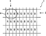
Fig. 2 is the schematic diagram of a part of the el display panel 1 of prior art.For the sake of clarity, some figure of this figure and back do not draw in proportion, and some parts amplifies.El display panel 1 comprises and a plurality ofly is arranged in rows 2 and the pixel 4 of row 3, forms lattice matrix in other words.Each pixel 4 in this example comprises red R, green G and three sub-pixels of blue B, can send redness, green and blue light when work respectively.In the el display panel that some matrixes are handled, just adopt this pixel arrangement.Image is for example lined by line scan, simultaneously appropriate signals is added to these and lists.
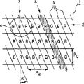
According to the present invention, the positional alignment of the sub-pixel that the positional alignment of the sub-pixel in each pixel and at least one neighbor are interior is different.Fig. 3 shows an embodiment of el display panel designed according to this invention.In this embodiment, the red, green, blue sub-pixel is along row 2 direction displacements.In the pixel 4 of row 3 and row 2 infalls, sub-pixel is arranged as green G, blue B and red R from left to right.In the pixel 6 of row 3 and row 5 infalls, sub-pixel is arranged as red R, green G and blue B from left to right.Therefore, two neighbors 4,6 in row 3 have different sub-pixel position to arrange in pixel.In addition, the sub-pixel R, the G that send same look at work of a plurality of pixels or B are adjacent to be arranged on the many parallel lines that are spaced laterally apart 7 of relative pixel grid pattern inclination.Sharp angle between the line 7 of vertical row 3 and inclination equals:
Wherein, n is the number of sub-pixels (n=3:R, G and B in this example) in the pixel, P
rBe be expert at pitch on 2,5 directions of pixel 4,6, and P
cBe the pitch of pixel 4,6 on row 3 directions.Pitch is the distance between the center of two neighbors 4,6.
Figure 4 and 5 show the result by Fig. 2 and 3 these two kinds of pixel arrangement emulation, are used for relatively having the el display panel of V seniority among brothers and sisters pixel arrangement (as shown in Figure 2) and have the situation of the el display panel of pixel arrangement (as shown in Figure 3) designed according to this invention.Though this pixel arrangement of Fig. 3 still has the RGB pattern (along line 7) of line sample association, compares with the image of Fig. 4, the picture quality of being felt of Fig. 5 just makes moderate progress.
In some el display panels 1 such as plasma display panel (PDP) and organic light-emitting diode (OLED) display screen, electroluminescent material deposits with the printing technology of for example ink jet printing and so on.If the line 8 that is a kind of electroluminescent material of particular color deposition can print continuously, it is the most fruitful adopting ink jet printing deposition sub-pixel R, G or B.Certainly, also can in position be interrupted inkjet deposited, but this can cause in manufacture process and inkjet mouth is navigated to some relevant problems of desired position on substrate.In addition, after the piezo nozzles in activating print head, in the formation spray is dripped, initial unsettled situation can occur, thereby cause making the luminescent material layer thickness that is deposited indefinite.Therefore advise sub-pixel not along row 3 printings, but tiltedly wear row 3.Fig. 6 shows the schematic diagram of an example of the pixel arrangement of being advised.In this embodiment of the present invention, 8 depositions along the line continuously do not need to deposit with position synchronous.Adopt this pixel arrangement, obtain a kind of arrangement of ternary sub-pixel, be similar to pixel arrangement shown in Figure 3 to a certain extent, yet avoided above-mentioned these problems relevant with the operation of ink jet printing machine.
The deposition electroluminescent material can tiltedly be worn the pattern guiding of the resistance bank (resistbank) of these row by some.Electroluminescent material is deposited between two resistance banks 9, prevents material mixing, and this can cause harmful and indefinite color mixture.
For these sub-pixels to the embodiment of Fig. 6 address, preferably adopt as shown in Figure 7 column electrode 10 and row electrode 11.Because these sub-pixels of Fig. 6 embodiment have the shape resemble the diamond block, so row electrode 11 can have the pattern of one-tenth scalariform as shown in Figure 7.
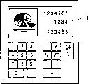
The picture quality of obviously improving lower resolution displays designed according to this invention is particularly conducive to handing or portable electric appts such as mobile phone, personal organizers and calculator.Fig. 8 to 10 shows such comprising as the example at the electronic equipment of the electroluminescent color display panel described in the claim 11: Fig. 8 shows and comprises the mobile phone of electroluminescent color display panel 1 designed according to this invention, Fig. 9 shows and comprises the calculator of electroluminescent color display panel 1 designed according to this invention, and Figure 10 shows and comprises the personal organizers of electroluminescent color display panel 1 designed according to this invention.
In general, the positional alignment of the interior sub-pixel of the positional alignment of the sub-pixel in each pixel of el display panel and at least one neighbor is different.This makes the beholder can feel to obtain the improvement of picture quality, particularly on lower resolution displays during the show events image.A preferred embodiment of the present invention is that arrangement of subpixels is at the el display panel of tiltedly wearing on some continuous lines of display screen.
It should be noted that the foregoing description is illustration the present invention, rather than restriction the present invention, the personnel that are familiar with this technical field can design many other implementations.For example, the function of row and row can be changed, and this does not deviate from the present invention.
The present invention also can be used for active matrix organic light emitting diode display, and wherein row electrode and column electrode are used for sub-pixel is addressed.
What is called " comprising " is not got rid of member or the step that also has other in embodiment those that show.
Claims (13)
1. one kind comprises a plurality of being arranged in rows, thereby the pixel of row forms the electroluminescent color display panel of lattice, each pixel comprises at least two sub-pixels, first sub-pixel wherein sends the light of first kind of color, and second sub-pixel sends the light of the second kind color different with first kind of color, and the feature of described electroluminescent color display panel is: the positional alignment of first and second sub-pixels in one first pixel in these pixels is different with the positional alignment of first and second sub-pixels in one of these pixels second pixel adjacent with described first pixel.
2. electroluminescent color display panel as claimed in claim 1, wherein said first pixel and second line of pixels are listed in the same row.
3. the electroluminescent color display panel described in claim 1 or 2, wherein said first sub-pixel are adjacent to be arranged on some parallel lines that are spaced laterally apart that relative column direction tilts.
4. electroluminescent color display panel as claimed in claim 3, first sub-pixel on the wherein said line that is arranged in an inclination forms a continuous bar that is made of electroluminescent material.
5. electroluminescent color display panel as claimed in claim 3, the line of wherein said inclination and acute angle between the vertical row are in that an optimum angle alpha+10 degree are to the scopes of-10 degree, and described optimum angle alpha equals:
Wherein, n is the number of sub-pixels in the pixel, P
rBe the pitch of pixel on line direction, and P
cBe the pitch of pixel on column direction.
6. electroluminescent color display panel as claimed in claim 1 or 2, one of them sub-pixel comprise a layer that is made of a kind of organic electroluminescent material.
7. electroluminescent color display panel as claimed in claim 6, wherein said organic electroluminescent material are a kind of polymer.
8. electroluminescent color display panel as claimed in claim 1 or 2, one of them sub-pixel comprise one by a kind of layer of constituting of fluorescent material that can the subject plasma discharge excitation.
9. method of making electroluminescent color display panel, described method comprises the following steps:
On a substrate, form a plurality of parallel first electrode strips that are spaced laterally apart,
Arrange a plurality of parallel electroluminescent bars that are spaced laterally apart, each light-emitting section sends the light of at least the first and second two kinds of a kind of colors in the color at work, and wherein the light-emitting section of different colours is configured to the pattern of a repetition side by side,
Form a plurality of parallel second electrode strips that are spaced laterally apart, these second electrode strips intersect with a plurality of first electrode strips, make at work luminescent device one by one be configured in the infall of first and second electrode strips,
It is characterized in that: described electroluminescent bar is configured on the many parallel lines that are spaced laterally apart that a relative grid that is formed by first and second electrode strips tilts.
10. method as claimed in claim 9, wherein said second electrode strip and the first electrode strip square crossing, thus obtain the grid of a rectangle that forms by these first and second electrode strips.
11. as claim 9 or 10 described methods, the acute angle between the line of wherein said first or second electrode strip and inclination be in an optimum angle alpha+10 to-10 the degree scopes in, described optimum angle alpha equals:
Wherein, n is the number of sub-pixels in the pixel, P
rBe the pitch of pixel on line direction, and P
cBe the pitch of pixel on column direction.
12. as claim 9 or 10 described methods, wherein said electroluminescent bar comprises a kind of organic electroluminescent material with ink jet printing machine deposition.
13. an electronic equipment, described electronic equipment comprise an electroluminescent color display panel as being proposed in claim 1.
Applications Claiming Priority (2)
| Application Number | Priority Date | Filing Date | Title |
|---|---|---|---|
| EP00204644.9 | 2000-12-20 | ||
| EP00204644 | 2000-12-20 |
Publications (2)
| Publication Number | Publication Date |
|---|---|
| CN1425267A CN1425267A (en) | 2003-06-18 |
| CN1295945C true CN1295945C (en) | 2007-01-17 |
Family
ID=8172472
Family Applications (1)
| Application Number | Title | Priority Date | Filing Date |
|---|---|---|---|
| CNB018083188A Expired - Fee Related CN1295945C (en) | 2000-12-20 | 2001-12-06 | Electroluminescent color display panel |
Country Status (8)
| Country | Link |
|---|---|
| US (1) | US6787987B2 (en) |
| EP (1) | EP1346610B1 (en) |
| JP (1) | JP2004516630A (en) |
| KR (1) | KR20020077448A (en) |
| CN (1) | CN1295945C (en) |
| AT (1) | ATE415802T1 (en) |
| DE (1) | DE60136740D1 (en) |
| WO (1) | WO2002051213A1 (en) |
Families Citing this family (35)
| Publication number | Priority date | Publication date | Assignee | Title |
|---|---|---|---|---|
| JP4789341B2 (en) * | 2001-03-30 | 2011-10-12 | 三洋電機株式会社 | Semiconductor device and mask for manufacturing semiconductor device |
| AU2003208531A1 (en) * | 2002-03-19 | 2003-09-29 | Koninklijke Philips Electronics N.V. | Plasma display panel electrode and phosphor structure |
| KR100459135B1 (en) * | 2002-08-17 | 2004-12-03 | 엘지전자 주식회사 | display panel in organic electroluminescence and production method of the same |
| DE10339772B4 (en) * | 2003-08-27 | 2006-07-13 | Novaled Gmbh | Light emitting device and method for its production |
| TWI402539B (en) * | 2003-12-17 | 2013-07-21 | Semiconductor Energy Lab | Display device and manufacturing method thereof |
| TWI251188B (en) * | 2004-03-31 | 2006-03-11 | Fuji Photo Film Co Ltd | Passive matrix light emitting device |
| TWI258721B (en) | 2004-08-10 | 2006-07-21 | Ind Tech Res Inst | Full-color organic electroluminescence device |
| JP4364849B2 (en) * | 2004-11-22 | 2009-11-18 | 三星モバイルディスプレイ株式會社 | Luminescent display device |
| KR100600345B1 (en) * | 2004-11-22 | 2006-07-18 | 삼성에스디아이 주식회사 | Pixel circuit and light emitting display using the same |
| US20060132028A1 (en) * | 2004-12-16 | 2006-06-22 | Lexmark International, Inc. | Electroluminescent display construction using printing technology |
| US7050697B1 (en) | 2004-12-29 | 2006-05-23 | E. I. Du Pont De Nemours And Company | Pixel arrangement for organic electronic devices |
| US7469638B2 (en) * | 2004-12-30 | 2008-12-30 | E.I. Du Pont De Nemours And Company | Electronic devices and processes for forming the same |
| KR100708147B1 (en) * | 2005-03-14 | 2007-04-16 | 삼성전자주식회사 | Light emitting cluster and direct light type back light unit and liquid display apparatus employing it |
| US7843134B2 (en) * | 2005-10-31 | 2010-11-30 | Idemitsu Kosan Co., Ltd. | Organic EL emission devices connected in series |
| KR101188429B1 (en) | 2005-12-30 | 2012-10-05 | 엘지디스플레이 주식회사 | Display panel removable colorbreak and stereoscopic 3-dimensional display device using thereof |
| US20070215883A1 (en) * | 2006-03-20 | 2007-09-20 | Dixon Michael J | Electroluminescent Devices, Subassemblies for use in Making Electroluminescent Devices, and Dielectric Materials, Conductive Inks and Substrates Related Thereto |
| KR20070095152A (en) * | 2006-03-20 | 2007-09-28 | 엘지전자 주식회사 | Light emitting device, shadow mask for light emitting device and fabrication method of light emitting device using the same |
| JP2008277264A (en) | 2007-04-03 | 2008-11-13 | Canon Inc | Color image display panel, manufacturing method therefor, and color image display device |
| KR100863963B1 (en) * | 2007-04-05 | 2008-10-16 | 삼성에스디아이 주식회사 | Organic light emitting diode display |
| KR100855020B1 (en) * | 2007-06-18 | 2008-08-28 | 성균관대학교산학협력단 | Apparatus and method for generating chain code |
| WO2009079004A1 (en) * | 2007-12-18 | 2009-06-25 | Lumimove, Inc., Dba Crosslink | Flexible electroluminescent devices and systems |
| US8716038B2 (en) | 2010-03-02 | 2014-05-06 | Micron Technology, Inc. | Microelectronic workpiece processing systems and associated methods of color correction |
| KR101097343B1 (en) | 2010-03-09 | 2011-12-23 | 삼성모바일디스플레이주식회사 | Organic light emitting display apparatus |
| RU2506654C2 (en) * | 2012-04-04 | 2014-02-10 | Закрытое акционерное общество Научно-технический центр "Альфа-М" | Method of displaying information on vertical displacement of shipborne landing strip when landing helicopter on ship |
| TWI509791B (en) * | 2013-05-22 | 2015-11-21 | Au Optronics Corp | Method for manufacturing an organic light emitting display panel and related organic light emitting display panel |
| WO2015091014A1 (en) | 2013-12-20 | 2015-06-25 | Koninklijke Philips N.V. | Autostereoscopic display device |
| CN103943656B (en) * | 2014-03-25 | 2017-01-18 | 京东方科技集团股份有限公司 | Organic light-emitting diode display pixel, display panel and display device |
| KR102170265B1 (en) | 2014-04-17 | 2020-10-26 | 삼성디스플레이 주식회사 | Display apparatus |
| KR102144767B1 (en) | 2014-06-02 | 2020-08-31 | 삼성디스플레이 주식회사 | Display panel and display apparatus including the same |
| CN104299974B (en) * | 2014-09-29 | 2017-02-15 | 京东方科技集团股份有限公司 | Array substrate, mask plate and display device |
| CN104282727B (en) * | 2014-09-30 | 2017-08-29 | 京东方科技集团股份有限公司 | A kind of dot structure and its display methods, display device |
| CN109983396B (en) * | 2016-11-17 | 2022-04-19 | 凸版印刷株式会社 | Reflective display device |
| CN109300936B (en) * | 2017-07-25 | 2021-04-06 | 上海和辉光电股份有限公司 | Display substrate, display panel and display device |
| CN111223902B (en) * | 2019-11-29 | 2022-06-17 | 云谷(固安)科技有限公司 | Pixel structure, mask and display device |
| WO2021199300A1 (en) * | 2020-03-31 | 2021-10-07 | シャープ株式会社 | Display device |
Citations (3)
| Publication number | Priority date | Publication date | Assignee | Title |
|---|---|---|---|---|
| CN1045904A (en) * | 1989-03-16 | 1990-10-03 | 菲利浦光灯制造公司 | Color monitor |
| EP0574084A1 (en) * | 1992-06-12 | 1993-12-15 | Koninklijke Philips Electronics N.V. | Flat-panel type picture display device with insulating electron-propagation ducts |
| EP0791847A1 (en) * | 1996-02-23 | 1997-08-27 | Koninklijke Philips Electronics N.V. | Autostereoscopic display apparatus |
Family Cites Families (14)
| Publication number | Priority date | Publication date | Assignee | Title |
|---|---|---|---|---|
| JP4142117B2 (en) | 1995-10-06 | 2008-08-27 | パイオニア株式会社 | Organic electroluminescence display panel and manufacturing method thereof |
| EP0883898B1 (en) * | 1996-12-03 | 2004-01-07 | Koninklijke Philips Electronics N.V. | Electric lamp with a coating displaying information, coating and marking ink for same |
| JPH10319870A (en) * | 1997-05-15 | 1998-12-04 | Nec Corp | Shadow mask and production for color thin film el display device using the same |
| KR100523869B1 (en) * | 1997-05-16 | 2005-12-29 | 엘지전자 주식회사 | Plasma Display Panel |
| US6008578A (en) * | 1998-02-20 | 1999-12-28 | Chen; Hsing | Full-color organic electroluminescent device with spaced apart fluorescent areas |
| US6140759A (en) * | 1998-07-17 | 2000-10-31 | Sarnoff Corporation | Embossed plasma display back panel |
| JP2000106276A (en) * | 1998-09-28 | 2000-04-11 | Fuji Photo Film Co Ltd | Full color luminescent device |
| JP2000228283A (en) * | 1999-02-05 | 2000-08-15 | Kawaguchiko Seimitsu Co Ltd | El and el aggregate |
| JP2001109401A (en) * | 1999-10-06 | 2001-04-20 | Matsushita Electric Ind Co Ltd | Color pixel array pattern as well as electrode pattern and electrode mask using the same |
| JP2001110574A (en) * | 1999-10-06 | 2001-04-20 | Matsushita Electric Ind Co Ltd | Electrode for light emitting element |
| JP3883770B2 (en) * | 2000-03-07 | 2007-02-21 | パイオニア株式会社 | Method for manufacturing light emitting device |
| JP4637391B2 (en) * | 2000-03-27 | 2011-02-23 | 株式会社半導体エネルギー研究所 | Method for manufacturing light emitting device |
| JP2001351787A (en) * | 2000-06-07 | 2001-12-21 | Sharp Corp | Organic led element, its manufacturing method and organic led display |
| JP2002075640A (en) * | 2000-08-30 | 2002-03-15 | Dainippon Screen Mfg Co Ltd | Manufacturing method of an organic el display device and its manufacturing device |
-
2001
- 2001-12-06 DE DE60136740T patent/DE60136740D1/en not_active Expired - Fee Related
- 2001-12-06 AT AT01271790T patent/ATE415802T1/en not_active IP Right Cessation
- 2001-12-06 EP EP01271790A patent/EP1346610B1/en not_active Expired - Lifetime
- 2001-12-06 KR KR1020027010533A patent/KR20020077448A/en not_active Application Discontinuation
- 2001-12-06 CN CNB018083188A patent/CN1295945C/en not_active Expired - Fee Related
- 2001-12-06 WO PCT/IB2001/002400 patent/WO2002051213A1/en active Application Filing
- 2001-12-06 JP JP2002552374A patent/JP2004516630A/en active Pending
- 2001-12-13 US US10/023,401 patent/US6787987B2/en not_active Expired - Lifetime
Patent Citations (3)
| Publication number | Priority date | Publication date | Assignee | Title |
|---|---|---|---|---|
| CN1045904A (en) * | 1989-03-16 | 1990-10-03 | 菲利浦光灯制造公司 | Color monitor |
| EP0574084A1 (en) * | 1992-06-12 | 1993-12-15 | Koninklijke Philips Electronics N.V. | Flat-panel type picture display device with insulating electron-propagation ducts |
| EP0791847A1 (en) * | 1996-02-23 | 1997-08-27 | Koninklijke Philips Electronics N.V. | Autostereoscopic display apparatus |
Also Published As
| Publication number | Publication date |
|---|---|
| EP1346610A1 (en) | 2003-09-24 |
| WO2002051213A1 (en) | 2002-06-27 |
| US6787987B2 (en) | 2004-09-07 |
| DE60136740D1 (en) | 2009-01-08 |
| ATE415802T1 (en) | 2008-12-15 |
| JP2004516630A (en) | 2004-06-03 |
| KR20020077448A (en) | 2002-10-11 |
| US20020109457A1 (en) | 2002-08-15 |
| EP1346610B1 (en) | 2008-11-26 |
| CN1425267A (en) | 2003-06-18 |
Similar Documents
| Publication | Publication Date | Title |
|---|---|---|
| CN1295945C (en) | Electroluminescent color display panel | |
| CN104362170B (en) | Organic electroluminescence display appliance and driving method and related device thereof | |
| EP2950348B1 (en) | Pixel structure for oled display screen | |
| CN104319283B (en) | A kind of organic elctroluminescent device, its driving method and display unit | |
| CN106449710A (en) | Pixel structure and OLED display panel having same | |
| CN206163494U (en) | Structure, organic electroluminescence device , display device , mask slice are arranged to pixel | |
| EP2996106A1 (en) | Display substrate and driving method thereof, and display device | |
| CN106298865A (en) | Pixel arrangement structure, organic electroluminescence device, display device, mask plate | |
| CN108493221A (en) | A kind of pixel arrangement structure, display panel, mask plate component and evaporated device | |
| KR101691738B1 (en) | Display device | |
| CN107452778A (en) | Display base plate, display device and its display methods, mask plate | |
| CN104835832A (en) | Pixel arrangement structure, organic electroluminescent device, display device, and mask plate | |
| CN103715227A (en) | Display panel, driving method of display panel and display device | |
| CN203260585U (en) | Pixel structure for OLED display screen, metal masking plate of pixel structure, and OLED display screen | |
| CN109148543A (en) | A kind of dot structure and display panel | |
| CN106920832A (en) | A kind of dot structure, its preparation method and display panel | |
| US10777616B2 (en) | Pixel arrangement structure, pixel structure and production method thereof, array substrate, and display panel | |
| KR20190131580A (en) | Pixel Structures and OLED Display Panels | |
| CN112436048A (en) | Pixel structure, fine metal mask plate, display device and control method | |
| CN110224016A (en) | Dot structure and display panel | |
| CN106449725A (en) | Organic light-emitting display panel and organic light-emitting display device | |
| CN110867479A (en) | Array substrate, display panel and display device | |
| CN1738501A (en) | Full color organic electro-luminescent display panel | |
| CN210052744U (en) | Pixel arrangement structure, color film structure and display panel | |
| CN108511482A (en) | Dot structure, mask plate and display device |
Legal Events
| Date | Code | Title | Description |
|---|---|---|---|
| C06 | Publication | ||
| PB01 | Publication | ||
| C10 | Entry into substantive examination | ||
| SE01 | Entry into force of request for substantive examination | ||
| C14 | Grant of patent or utility model | ||
| GR01 | Patent grant | ||
| C17 | Cessation of patent right | ||
| CF01 | Termination of patent right due to non-payment of annual fee |
Granted publication date: 20070117 Termination date: 20100106 |