Active matrix display device
Technical field
The present invention relates to a kind of display device, specifically, relate to a kind of active array type display apparatus that on its substrate surface, has display driver circuit.
Background technology
Illustrate, in the active array type liquid crystal display, on the liquid crystal side surface of a substrate of a pair of substrate that is arranged to face with each other through liquid crystal, form a plurality of pixel areas, wherein around described pixel area, form a plurality of signal lines and drain signal line, described signal line is arranged in parallel with each other along the directions X extension and along the Y direction, and described drain signal line is arranged in parallel with each other along the extension of Y direction and along directions X.
Each pixel area has sheet resistance and pixel capacitors, and described sheet resistance receives sweep signal from the signal line, and the described sheet resistance of described pixel capacitors process provides the vision signal from described drain signal line.
This pixel capacitors forms electric field in described pixel capacitors with between the opposite electrode that forms on another substrate side for example, and the light of the described liquid crystal that inserts between described electrode by this electric field controls is propagated.
This liquid crystal display has and is used for sweep signal is offered the scan signal drive circuit of signal line separately, and has and be used for vision signal is offered the video signal line driving circuit of drain signal line separately.
From described scan signal drive circuit and described video signal driver is by a large amount of and the angle that constitutes at the inner similar MIS transistor of thin film transistor (TFT) that forms of pixel area, known wherein these transistorized semiconductor layers be form by polysilicon (P-Si) with described scan signal drive circuit and video signal line driving circuit the technology that on the surface of single substrate, forms that forms with described pixel.
Described scan signal drive circuit is the circuit that mainly uses shift register, and described video signal line driving circuit also uses as its a part of shift register.
But with regard to shift register, current needs can work in high speed, low pressure, low-power consumption, and do not have the shift register of through current.In order to satisfy this demand, for example advised a kind of shift register that is referred to as the dynamic ratio shift register.
Fig. 9 A shows the structure that for example discloses this dynamic ratio shift register of No 45638/1987 disclosure at Jap.P..
In addition, Fig. 9 B shows the sequential chart of circuit shown in Fig. 9 A, and wherein, this sequential chart shows the node N1 corresponding with input pulse φ IN and synchronizing pulse φ 1, φ 2 and the corresponding output VN1 and the VN6 at N6 place.
At first, when synchronizing pulse φ 1 at time t1 place when low level (after this being referred to as " L ") is changed into high level (after this being referred to as " H "), input pulse φ IN become " H " and therefore the current potential VN1 of node N1 become " H " through NMT1 from " L ".
" L " that suppose input pulse φ IN and have synchronizing pulse φ 1, the φ 2 of opposite phase each other be the threshold value Vth of V φ<NMT1 for " H " of ground level (GND) and input pulse φ IN and synchronizing pulse φ 1, φ 2, and current potential VN1 can be expressed as following equation (1) basically at this moment.Here, V φ represents the voltage that is in " H " of synchronizing pulse φ 1, φ 2, and NMT1 represents MOS transistor.
VN1=Vφ-Vth …(1)
Even when state in time t2 place synchronizing pulse φ 1 drop to " L " from " H ", when input pulse φ IN is maintained at " H ", output VN1 also keeps (being said on the meaning of strictness by the voltage of equation (1) expression, at the time point place that described synchronizing pulse φ 1 descends, because in the grid of described NMT1 and the capacitive coupling between the node N1, described current potential becomes and is lower than the voltage of equation (1) expression.But this phenomenon is not main in entire work process, therefore can ignore this phenomenon).Because described NMT1 becomes and ends, node N1 becomes unsteady point.
Subsequently, when synchronizing pulse φ 2 at time t2 place when " L " becomes " H ", if satisfy following equation (2):
Vφ-Vth≥Vφ …(2)
So, MOS transistor NMT2 becomes conducting state and pulse φ 2 enters node N2.
At this moment, because the coupling capacitance cb1 that is referred to as bootstrap capacitor that inserts between node N1 and N2, the rising of voltage is transmitted to the node N1 that is in quick condition on the node N2 point, thereby the current potential of node N2 is also raise.
Suppose that the current potential that node N2 raises is Δ VN2, so, equation (3) provides output VN1:
VN1=(Vφ-Vth)+ΔVN2(cb/cb(cb+cs)) …(3)
Here, except that such as preceding CB1 with beyond the electric capacity shown in the described circuit, electric capacity cb comprises all coupling capacitances of synchronizing pulse φ 2 and node N1, comprises that the electric capacity that the inversion layer (raceway groove) that forms by grid, drain electrode and the source electrode of NMT2 or under by described grid produces also is included in the direct connection electric capacity that connects up between described synchronizing pulse φ 2 and the node N1.In addition, Cs represents by deduct the electric capacity that above-mentioned bootstrap capacitor Cb obtained and be referred to as stray capacitance from the whole capacitor of node N1 afterwards.
Here, suppose and under the situation of Δ VN2 V φ, satisfy equation (4):
(Vφ-Vth)+Vφ(Cb/Cb(Cb+Cs))>Vφ+Vth …(4)
This means the grid voltage of MOS transistor NMT2, promptly export VN1 and become and be higher than V φ+Vth.Therefore, described VN2 is set to the current potential of voltage V φ.
By suitably selecting to constitute the capacitor C b1 of design element, can satisfy above-mentioned equation (4) at an easy rate, therefore, output VN2 can be set to the current potential of voltage V φ.
At this moment, the current potential of node N3 is got the value of equation (5) expression through the MOS transistor NMT3 that is connected with diode.
VN3=VφVth …(5)
Because MOS transistor NMT3 is carried out second tube sheet and connects, so even when synchronizing pulse φ 2 at time t3 place when " H " becomes " L ", also can keep the state of representing by equation (5).
When synchronizing pulse φ 1 at time t3 place when " L " becomes " H ", take place at node N3 and MOS transistor NMT5 place with by similar operation shown in the equation (3), thereby output VN3, VN4 produce the potential change shown in Figure 1B respectively.
Here,, the shift pulse (VN2, VN4, VN6) that its current potential equals " H " of described synchronizing pulse can be obtained, and when carrying out aforesaid operations, the dynamic operation that does not produce through current can be carried out as node N2, N4, when N6 is used as output node.
But, when directly offering by the MIS transistor that will have the semiconductor layer of making by polysilicon (P-Si) when being arranged to each other substrate (glass substrate) surface of facing through liquid crystal, describedly dynamically will work in very unsettled mode, thereby need to deal with the countermeasure of this phenomenon than register.
Promptly, electric capacity when the floating node such as node N1, N3 is in " L " is very little, and other electric capacity that comprise node N1, the N2 of Cdg1, Cdg2, compare with the coupling capacitance between the drain electrode grids such as synchronizing pulse and node N1, N3, as very little shown at Cdg1, the Cdg2 of Fig. 9 A, thus, exist very big possibility to make non-selected transistor also become " conducting " state.When described circuit kept original state, design and operating voltage were restricted to maintenance and " end " state.
Be located on described glass substrate the single crystal semiconductor that forms and located by the dynamic non-ratio shift register (dynamic ratioless shift register) that thin film transistor (TFT) is made, the main cause that electric capacity becomes very little when floating node is in " L " state is as follows.
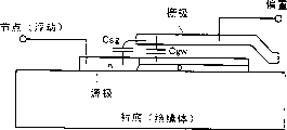
Figure 10 A shows the sectional view of the n-type MOS transistor that forms on single crystal semiconductor.Have the SIC (semiconductor integrated circuit) that constitutes described semi-conductive substrate and be used for element separation etc. with the form use (comprising ground connection) that is biased usually.
Therefore, shown in Figure 10 A, depletion-layer capacitance Csw through the formation of the reverse bias between source (diffusion layer) and trap (or substrate), the drain electrode and described trap between depletion-layer capacitance Cdw and between grid and described trap capacitor C gw, described source electrode, drain and gate and described trap capacitive coupling.In addition, described wiring also with described substrate or be set directly at described trap capacitive coupling under the winding with capacitor C lw through thick insulating film.These electric capacity belong to the one group of electric capacity that is referred to as stray capacitance usually.
Therefore, partly locate at the node N3 shown in Fig. 9 A because the capacitor C lw (Clw3) of the wiring of the capacitor C sw (Csw7) of the capacitor C gw (Cgw6) of capacitor C sw (Csw3), the NMT6 of NMT3, capacitor C dw (Cdw6), NMT7 and this node of formation can obtain and described trap between big coupling capacitance.
In addition, constitute by the mos capacitance that makes described bootstrap capacitor have the reinforcement shown in Figure 10 B and the 10C, described trap is by capacitive ground and the inversion layer coupling that constitutes the depletion layer extension of isolating node from " ON " time shown in Figure 10 B, thereby obtain enough bootstrapping effects (bootstrapping effect), simultaneously at the electric Cb1 (W) of the place's acquisition of " OFF " time shown in Figure 10 B with described trap coupling.
Therefore, when node N3 is in " L ",, also can utilize the biasing of the described trap of the above-mentioned coupling capacitance of process to guarantee big electric capacity even when node N3 floats in the circuit shown in Fig. 9 A.With regard to these electric capacity, the Cdw of NMT3 (Cdwl) and the wiring of φ 1 and the space capacitor C l φ 1 between the node N3 and enough little, therefore, when the potential difference (PD) Δ NV3 of wiring φ 1 node N3 when " L " becomes " H " is represented by following equation (6) basically:
ΔVN3=Vφ×(Cdw+Clφl)/(Cdw1|Clφ2+Csw3+Cgw6+Cdw6+Csw7+Cb1(W))
…(6)
In addition, as explaining in the above, owing to set up the relation of representing by equation (7):
Cdw1+Clφ2<<Csw3+Cgw6+Cdw6+Csw7+Cb1(W) …(7)
So, be easy to satisfy following equation (8).
ΔVN3<Vth …(8)
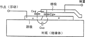
But, when on glass substrate, forming the similar circuit of making by the monocrystal thin films transistor, can not realize above-mentioned operation.
That is, Figure 10 D shows the transistorized sectional view of the monocrystal thin films that forms on described glass substrate.Suppose that described substrate is formed by insulator, so, in case the p layer of arranging under source electrode, drain and gate becomes unsteady, so, the electric capacity that can be coupled will become depletion-layer capacitance Cdp, Csp between described source electrode, drain electrode or grid and the described p layer arranged under described source electrode, drain electrode or the grid or between described p layer and the described wiring that is provided with away from described source electrode, drain electrode or grid very little space capacitor C s1, Cp1, Cd1.For the part of the node N3 that gets circuit shown in Fig. 9 A in the mode identical with above-mentioned example as an example, node N3 is capacitively coupled to node N2 through the source Csp3 of described MOS transistor NMT3.Because node N2 also floats, so the path is divided into introduces described electric capacity with the path of node N1 coupling with through the SP2 of described MOS transistor NMT2 and the path of synchronizing pulse φ 2 couplings through capacitor C b1.Because node N1 also floats, so the path is divided into capacitor C sp4 and the capacity coupled path of earth potential Vss through the capacitor C sp1 of described MOS transistor NMT1 and capacity coupled path of input pulse φ IN and the described MOS transistor NMT4 of process, the capacitor C sp4 of described MOS transistor NMT4 is through the capacitor C sg1 introducing of described MOS transistor NMT1 and the capacitive coupling of synchronizing pulse φ 1.
That is, two electric capacity also becomes very little and to be coupled when synchronizing pulse φ 1 mode that output VN3 is booted when " L " becomes " H " and the function of synchronizing pulse φ 1.
Though the source electrode of MOS transistor NMT7 is through capacitor C sp7 and earth potential VSS coupling, this is unessential.In addition, node N3 process capacitor C b2 and node N4 capacitive coupling, thus node N4 is also floated.The wiring of configuration node N3 does not have the directly electric capacity under node N3, and node N3 only has the weak capacitive through described space electric capacity and arbitrary wiring coupling.
Node N3 is through capacitor C dg5 and synchronizing pulse φ 1 capacitive coupling of MOS transistor NMT5.This capacitive coupling is and the direct coupling of outside and relatively large.This electric capacity becomes unsettled reason.
The summation of supposing the auxiliary coupling capacitance of above-mentioned node N3 except capacitor C dg5 is used as capacitor C N3, so, and when the potential change Δ VN3 of synchronizing pulse φ 1 node N3 when " L " becomes " H " is represented by following equation (9) basically.Because it is above-mentioned so big that capacitor C N3 does not have, so, on the basis of the value (the W size design of MOS transistor NMT5 or the distributing of synchronizing pulse φ 1) of voltage V φ and capacitor C dg5, can be introduced at an easy rate by the described condition of following equation (10).
ΔVN3=Vφx(Cdg5/(Cdg5+CN3)) …(9)
ΔVN3≥Vth …(10)
In case satisfy the condition that equation (10) is pointed out, the capacitor C gp of MOS transistor NMT5 (utilizing the electric capacity of described inversion layer) and bootstrap capacitor Cb2 are changed the electric capacity that is coupled with opposite way and node N3 and described φ 1, thereby the possibility that causes MOS transistor NMT3 to become complete conducting state owing to described bootstrapping effect has increased greatly.
That is, produced unsettled work, the feasible and incoherent node of controlled node has all become " H " and has produced output or begin scanning from this part.
The present invention is from such angle, and purpose of the present invention just provides a kind of display device with dynamic relationship shift register that can guarantee steady operation and can increase design freedom.
Summary of the invention
The brief summary of the invention in the middle of the invention that once in Ben Dingming, discloses of simplicity of explanation at first.It is summarized as follows.
According to the present invention, a kind of display device is provided, it is characterized in that:
Described display device has and comprises the driving circuit that is formed on the shift register on the substrate surface, and described shift register is made of first to the 7th MISTFT that uses polysilicon as semiconductor layer, among described first to the 7th MISTFT each all has first end and second end, wherein
First end of a described MISTFT is connected on the input pulse, and the gate terminal of a described MISTFT is connected on first synchronizing pulse, forms the importation thus,
Second end of a described MISTFT is connected to the gate terminal of described the 2nd MISTFT and first end of described the 4th MISTFT, also is connected to first end of first capacity cell,
Second end of described first capacity cell is connected to fixed voltage, and first end of described the 2nd MISTFT is connected to second synchronizing pulse anti-phase with described first synchronizing pulse,
Second end of described the 2nd MISTFT is connected to first end and the gate terminal of described the 3rd MISTFT, also is connected to first end of second capacity cell,
Second end of described second capacity cell is connected to second end of a described MISTFT, the gate terminal of the 2nd MISTFT and first end of described the 4th MISTFT,
Second end of described the 3rd MISTFT is connected to the gate terminal of described the 5th MISTFT and first end of the 7th MISTFT, and is connected with first end of the 3rd capacity cell, forms one first output terminal thus,
Described the 3rd electric capacity second end be connected to fixed voltage, and first end of described the 5th MISTFT is connected to described first synchronizing pulse,
Second end of described the 5th MISTFT is connected to the gate terminal of first end and gate terminal and described the 4th MISTFT of described the 6th MISTFT, also is connected to first end of the 4th electric capacity, forming one second output terminal,
Second end of described the 4th electric capacity be connected to the gate terminal of second end, the 5th MISTFT of described the 3rd MISTFT and the 7th MISTFT first end and
Second end of described the 4th MISTFT and second end of described the 7th MISTFT are connected to fixed power source or earth potential,
Wherein, being shifted the gate terminal that a clock and the pulse corresponding with the pulse of the gate terminal that inputs to described the 4th MISTFT input to described the 7th MISTFT.
In having the display device of this structure, an end of load capacitance is connected on the node that can float.The other end of described load capacitance is connected on set potential or the similar current potential.Therefore, can relax, thereby make it possible to achieve the shift register of the stable dynamic relationship that comprises the thin film transistor (TFT) of making by polysilicon in the design tolerances that above-mentioned unstable element is suppressed under the state.
According to above-mentioned display device of the present invention, it is characterized in that: n basic circuit is by multistage connection, and each basic circuit wherein all is made of second to the 7th MISTFT and first to the 4th electric capacity,
The gate terminal of the MISTFT corresponding with the 2nd MISTFT of i basic circuit is connected to second end with the corresponding MISTFT of the 6th MISTFFT of (i-1) individual basic circuit,
The gate terminal of the described MISTFT corresponding with the 7th MISTFT of described i basic circuit be connected to second end of the corresponding described MISTFT of the 2nd MISTFT of (i+1) individual basic circuit and
Pulse corresponding with the pulse of the gate terminal of the 4th MISTFT that inputs to the next stage basic circuit and that be shifted a clock be transfused to the gate terminal of the corresponding described MISTFT of the 7th MISTFT of n basic circuit.
According to display device of the present invention, its feature is that also described the 2nd MISTFT is inserted in first basic circuit, a described MISTFT and the 2nd MISTFT be inserted into second and each of follow-up basic circuit in the middle of,
The gate terminal of a described MISTFT is connected to the input end of described input pulse, its first end is connected to the gate terminal of the MISTFT corresponding with described the 2nd MISTFT, its second end is connected on fixed power source or the earth potential, described fixed power source or earth potential equal a voltage, this voltage will be the source voltage that is included in the described MISTFT in the middle of the voltage of described first and second synchronizing pulses, it maybe will be the source voltage of described first and second synchronizing pulses, and be not less than the threshold voltage of described the 4th MISTFT, and
The gate terminal of described the 2nd MISTFT is connected to the input end of described input pulse, its first end is connected to the gate terminal of described the 5th MISTFT or the gate terminal of the MISTFT corresponding with described the 5th MISTFT, its second end is connected to fixed power source or earth potential, described fixed power source or earth potential equal a voltage, this voltage will be the source voltage that is included in the described MISTFT in the voltage of described first and second synchronizing pulses, to be the source voltage of described first and second synchronizing pulses maybe, and be not less than the threshold voltage of described the 4th MISTFT.
According to the present invention, a kind of display device is provided, it is characterized in that:
Described display device has and comprises the driving circuit that is formed on the shift register on the substrate surface, described shift register is made of first to the 7th MISTFT that uses polysilicon as semiconductor layer, among described first to the 7th MISTFT each all has first end and second end, wherein
First end and the gate terminal of a described MISTFT are connected on the input pulse, form the importation thus,
Second end of a described MISTFT is connected to the gate terminal of described the 2nd MISTFT and first end of described the 4th MISTFT, also is connected to first end of first capacity cell,
Second end of described first electric capacity is connected to fixed voltage, and first end of described the 2nd MISTFT is connected to second synchronizing pulse anti-phase with first synchronizing pulse,
Second end of described the 2nd MISTFT is connected to first end and the gate terminal of described the 3rd MISTFT, also is connected to first end of second electric capacity,
Second end of described second electric capacity is connected to the gate terminal of second end of a described MISTFT, described the 2nd MISTFT and first end of described the 4th MISTFT,
Second end of described the 3rd MISTFT is connected to the gate terminal of described the 5th MISTFT and first end of described the 7th MISTFT, also is connected to first end of the 3rd capacity cell, forms one first output terminal thus,
Second end of described the 3rd electric capacity is connected to fixed voltage, and first end of described the 5th MISTFT is connected to described first synchronizing pulse,
Second end of described the 5th MISTFT is connected to the gate terminal of first end and gate terminal and the 4th MISTFT of described the 6th MISTFT, also is connected to first end of the 4th electric capacity, forms one second output terminal thus,
Second end of described the 4th electric capacity is connected to second end of described the 3rd MISTFT, the gate terminal of the 5th MISTFT and first end of described the 7th MISTFT, and
Second end of described the 4th MISTFT and second end of described the 7th MISTFT are connected to fixed power source or earth potential,
Wherein, being shifted the gate terminal that a clock and the pulse corresponding with the pulse of the gate terminal that inputs to described the 4th MISTFT input to described the 7th MISTFT.
Above-mentioned display device according to the present invention is characterised in that n basic circuit is by multistage connection, and wherein each all is made of second to the 7th MISTFT and first to the 4th electric capacity,
The gate terminal of the described MISTFT corresponding with the 2nd MISTFT of i basic circuit is connected to second end with the corresponding described MISTFT of the 6th MISTFT of (i-1) individual basic circuit,
The gate terminal of the described MISTFT corresponding with the 7th MISTFT of described i basic circuit is connected to second end with the corresponding described MISTFT of the 2nd MISTFT of (i+1) individual basic circuit, and pulse corresponding with the pulse of the gate terminal of the 4th MISTFT that inputs to the described basic circuit of next stage and that be shifted a clock be transfused to the gate terminal of the corresponding described MISTFT of the 7th MISTFT of n basic circuit.
Feature according to display device of the present invention is that also described the 2nd MISTFT is inserted in first basic circuit, a described MISTFT and described the 2nd MISTFT be inserted into described second and each of follow-up basic circuit in the middle of,
The gate terminal of a described MISTFT is connected to the input end of described input pulse, its first end is connected to the gate terminal of the described MISTFT corresponding with described the 2nd MISTFT, be connected to fixed power source or earth potential with its second end, described fixed power source or earth potential equal a voltage, this voltage will be the source voltage that is included in the described MISTFT in the middle of the voltage of described first and second synchronizing pulses, it maybe will be the source voltage of described first and second synchronizing pulses, and be not less than the threshold voltage of described the 4th MISTFT, and
The grid of described the 2nd MISTFT is connected to the input end of described input pulse, be connected to the gate terminal of described the 5th MISTFT or the gate terminal of the MISTFT corresponding with its first end with described the 5th MISTFT, its second end is connected to fixed power source or earth potential, described fixed power source or earth potential equal a voltage, this voltage will be the source voltage that is included in the described MISTFT in the middle of the voltage of described first and second synchronizing pulses, to be the source voltage of described first and second synchronizing pulses maybe, and be not less than the threshold voltage according of described the 4th MISTFT.
The present invention also provides a kind of display device, it is characterized in that:
Described display device has the driving circuit that comprises the lip-deep shift register that is formed on substrate, constitute by first to the 7th MISTFT that uses polysilicon as semiconductor layer with described shift register, among described first to the 7th MISTFT each all has first end and second end, wherein
First end and the gate terminal of a described MISTFT are connected to input pulse, form the importation thus,
Second end of a described MISTFT is connected to the gate terminal of described the 2nd MISTFT and first end of described the 4th MISTFT, also is connected to fixed voltage through first electric capacity,
First end of described the 2nd MISTFT is connected to second synchronizing pulse anti-phase with first synchronizing pulse,
Second end of described the 2nd MISTFT is connected to first end and the gate terminal of described the 3rd MISTFT, also is connected to second end of a described MISTFT, the gate terminal of the 2nd MISTFT and first end of the 4th MISTFT through second electric capacity,
Second end of described the 3rd MISTFT is connected to the gate terminal of described the 5th MISTFT and first end of the 7th MISTFT, also is connected to described fixed voltage through the 3rd capacity cell,
First end of described the 5th MISTFT is connected to described first synchronizing pulse,
Second end of described the 5th MISTFT is connected to the gate terminal of first end and gate terminal and the 4th MISTFT of the 6th MISTFT, also be connected to second end of the 3rd MISTFT, the gate terminal of the 5th MISTFT and first end of the 7th MISTFT through the 4th electric capacity, and
Second end of the 4th MISTFT is connected to fixed power source or earth potential,
Wherein, being shifted the gate terminal that a clock and the pulse corresponding with the pulse of the gate terminal that inputs to described the 4th MISTFT input to described the 7th MISTFT.
According to above-mentioned display device of the present invention, n basic circuit is by multistage connection, and wherein each all is made of second to the 7th MISTFT and first, second electric capacity,
The gate terminal of the described MISTFT corresponding with the 2nd MISTFT of i basic circuit is connected to second end with the corresponding described MISTFT of the 6th MISTFT of (i-1) individual basic circuit,
The gate terminal of the described MISTFT corresponding with the 7th MISTFT of described i basic circuit is connected to second end with the corresponding described MISTFT of the 6th MISTFT of (i+1) individual basic circuit.
The invention provides another kind of display device, it is characterized in that:
Described display device has and comprises the driving circuit that is formed on the shift register on the substrate surface, described shift register is made of the first to the 11 MISTFT that uses polysilicon as semiconductor layer, described the first to the 11 MISFE has first end and second end, wherein
First end of a described MISTFT is connected to input pulse,
The gate terminal of a described MISTFT is connected to first synchronizing pulse, forms the importation thus,
Second end of a described MISTFT is connected to the gate terminal of described the 4th MISTFT and first end of described the 3rd MISTFT, also is connected to first end of first electric capacity,
Second end of described first electric capacity is connected to second end of described the 4th MISTFT, first end of the 5th MISTFT and first end and the gate terminal of gate terminal and the 6th MISTFT, also is connected to the gate terminal of described the 7th MISTFT,
The gate terminal of described the 2nd MISTFT is connected to described input pulse,
First end of described the 2nd MISTFT is connected to the gate terminal of second end and the 3rd MISTFT of the 11 MISTFT,
Second end of described the 2nd MISTFT and second end of described the 7th MISTFT are connected to fixed power source or earth potential, described fixed power source or earth potential equal a voltage, this voltage will be the source voltage that is included in the described MISTFT in the middle of the voltage of described first and second synchronizing pulses, it maybe will be the source voltage of described first and second synchronizing pulses, and be not less than the threshold voltage of described the 4th MISTFT
Second end of described the 3rd MISTFT is connected to fixed power source or earth potential, described fixedly electricity or earth potential equal a voltage, this voltage will be that the source voltage that is included in the described MISTFT in the middle of the voltage of described first and second synchronizing pulses maybe will be the source voltage of described first and second synchronizing pulses, and be not less than the threshold voltage according of described the 4th MISTFT
First end of described the 4th MISTFT is connected to described second synchronizing pulse,
Second end of described the 5th MISTFT is connected to the gate terminal of described the 9th MISTFT and first end of described the 8th MISTFT,
First end of second end of described the 9th MISTFT, first end of the tenth MISTFT and gate terminal and the 11 MISTFT and second end that gate terminal is connected to second electric capacity,
First end of described the 7th MISTFT is connected to the gate terminal of described the 8th MISTFT, and second end of described the 8th MISTFT is connected to fixed power source or earth potential, and
First end of described the 9th MISTFT is connected to described first synchronizing pulse, wherein is shifted a clock and the pulse corresponding with the pulse of the gate terminal that inputs to described the 4th MISTFT and is transfused to the gate terminal of described the 8th MISTFT and first end of described the 7th MISTFT.
According to above-mentioned display device of the present invention, n basic circuit be by multistage connection, wherein each all be by second, third, the 4th, the 5th, the 7th, the 8th, the 9th and the tenth MISTFT and first and second electric capacity constitute,
Second end of the MISTFT corresponding with the tenth MISTFT of i basic circuit is connected to the gate terminal with the corresponding MISTFT of the 4th MISTFT of (i+1) individual basic circuit, second end of the described MISTFT corresponding with described the 7th MISTFT and be connected to the corresponding electric capacity of first electric capacity with (i+1) individual basic circuit through described the 6th MISTFT with the gate terminal of the corresponding MISTFT of the 8th MISTFT of described i basic circuit.
Above-mentioned display device according to the present invention is characterised in that: at the basic circuit separately that begins from described second basic circuit, second end that its first end and gate terminal are connected to the described MISTFT on the input pulse is connected on second end of the MISTFT corresponding with described the 11 MISTFT
At the basic circuit separately that begins from described the 3rd basic circuit, second end that its first end and gate terminal are connected to described the 2nd MISTFT of input pulse is connected to the gate terminal of the MISTFT corresponding with the 8th MISTFT of the basic circuit that forms target basic circuit prestage, and be connected on second end of an electric capacity corresponding with described first electric capacity through described MISTFT, and
Described second end of described MISTFT is connected to second end of described the 2nd MISTFT, and described first end and gate terminal are connected on the described electric capacity.
Also provide a kind of display device according to the present invention, it is characterized in that:
Described display device has and comprises the driving circuit that is formed on the shift register on the substrate surface, described shift register is made of the first to the 11 MISTFT that uses polysilicon as semiconductor layer, among described the first to the 11 MISTFT each all comprises first end and second end, wherein
First end and the gate terminal of a described MISTFT are connected to input pulse, form the importation thus,
Second end of a described MISTFT is connected to the gate terminal of described the 4th MISTFT and first end of described the 3rd MISTFT, also is connected to first end of first electric capacity,
Second end of described first electric capacity is connected to first end and the gate terminal of first end and gate terminal and the 6th MISTFT of second end of described the 4th MISTFT, described the 5th MISTFT, also is connected to the gate terminal of described the 7th MISTFT,
The gate terminal of described the 2nd MISTFT is connected to described input pulse,
First end of described the 2nd MISTFT is connected to the gate terminal of second end and the 3rd MISTFT of the 11 MISTFT,
Second end of described the 2nd MISTFT and second end of described the 7th MISTFT are connected to fixed power source or earth potential,
Second end of described the 3rd MISTFT is connected to fixed power source or earth potential,
First end of described four MISTFT is connected to described second synchronizing pulse,
Second end of described the 5th MISTFT is connected to the gate terminal of described the 9th MISTFT and first end of the 8th MISTFT,
Second end of described second electric capacity is connected to first end and the gate terminal of first end and gate terminal and described the 11 MISTFT of second end of described the 9th MISTFT, described the tenth MISTFT,
First end of described the 7th MISTFT is connected to the gate terminal of described the 8th MISTFT,
Second end of described the 8th MISTFT is connected to fixed power source or earth potential, and
First end of described the 9th MISTFT is connected to described first synchronizing pulse, wherein is shifted a clock and the pulse corresponding with the pulse of the gate terminal that inputs to described the 3rd MISTFT and is transfused to the gate terminal of described the 8th MISTFT and first end of described the 7th MISTFT.
According to above-mentioned display device of the present invention, it is characterized in that n basic circuit by multistage connection, wherein each all by second, third, the 4th, the 5th, the 7th, the 8th, the 9th and the tenth MISTFT and first and second electric capacity constitute,
Second end of the MISTFT corresponding with the tenth MISTFT of i basic circuit is connected to the gate terminal with the corresponding described MISTFT of the 4th MISTFT of (i+1) individual basic circuit, second end of the MISTFT corresponding with described the 7th MISTFT and be connected to the corresponding electric capacity of first electric capacity with (i+1) individual basic circuit through described the 6th MISTFT with the gate terminal of the corresponding MISTFT of the 8th MISTFT of described i basic circuit.
According to above-mentioned display device of the present invention, it is characterized in that, at each the basic circuit place since second basic circuit, second end that its first end and gate terminal are connected to the described MISTFT on the input pulse is connected to second end of the MISTFT corresponding with described the 11 MISTFT
At each basic circuit place since the 3rd basic circuit, second end that its first end and gate terminal are connected to the 2nd MISTFT on the input pulse is connected to the gate terminal of the MISTFT corresponding with the 8th MISTFT of the basic circuit that forms described target basic circuit, and the described MISTFT of process is connected to and second end of the electric capacity that a described low electric capacity is corresponding, and
Second end of described MISTFT is connected to second end of described the 2nd MISTFT and described first end and gate terminal and is connected to described electric capacity.
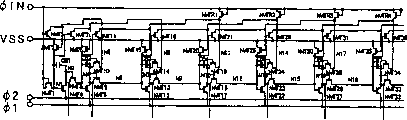
Another kind of display device according to the present invention is characterised in that: for example have the disproportional dynamic shift register that is positioned on the substrate surface, this disproportional dynamic shift register comprises multistage phase inverter,
Described disproportional dynamic shift register is made of a plurality of MISTFT that use polysilicon as semiconductor layer,
Each MISTFT is connected in parallel on the ground level of outputs at different levels, and
Constitute described each MISTFT, so that make each output drop to ground level during as the cycle the cycle of the input signal transmission of phase inverter high level at the level place before the level that is constituting described MISTFT.
Display device according to the present invention is characterised in that for example under the prerequisite of means 15 structures, each MISTFT is operated in output by the input next stage, during the cycle of stating in the described level place before the level that is wherein constituting described MISTFT cycle of input signal transmission that high level signal is used as described phase inverter, each output drops to ground level.
Means 17.
Display device according to the present invention is characterised in that for example under the prerequisite of means 15, operate each MISTFT by input clock pulse, during the cycle of stating in the described level place before the level that is constituting described MISTFT the cycle that high level signal is used as described phase inverter input signal transmission, each output drops to earth potential.
Means 18.
Display device according to the present invention is characterised in that for example described display device has the display driver circuit that comprises the disproportional dynamic shift register, and described disproportional dynamic shift register is included in the multistage phase inverter that forms on the substrate surface,
Described disproportional dynamic shift register is made of a plurality of MISTFT that use polysilicon as semiconductor layer,
A described MISTFT who is connected in parallel with each other and the 2nd MISTFT are used as the MISTFT of the ground level that is connected to corresponding outputs at different levels and provide,
Any being constructed as follows among described first and second MISTFT, during cycle promptly stating cycle of input signal transmission that high level signal is used as described phase inverter in the level place before the described level that is constituting described MISTFT, each output drops to ground level, and
Any grid and have through diode between the node of clock the diode that constitutes the 3rd MISTFT is provided in a described MISTFT and described the 2nd MISTFT therefrom is leaked to described node and forms to because the current potential of described node drops to the negative-phase sequence curent that is lower than the caused described diode of described ground level thereby avoided being used for electric charge to described gate charges.
Means 19.
Display device according to the present invention is characterised in that for example described display device has the display driver circuit that comprises the disproportional dynamic shift register, and described disproportional dynamic shift register is included in the multistage phase inverter that forms on the substrate surface,
Described disproportional dynamic shift register constitute by a plurality of MISTFT that use polysilicon as semiconductor layer and
The 3rd MISTFT and the 4th MISTFT that the described MISTFT that corresponding output at different levels is reduced to ground level when a described low clock and second clock are in " ON " state and described the 2nd MISTFT are provided and when described output is in " height " level, have become " ON " state and a described MISTFT and the 2nd MISTFT are ended.
Means 20.
Display device according to the present invention is characterised in that for example under the prerequisite of means 19 structures, described first clock is inputed to the grid of a described MISTFT through described first capacity cell, described second clock is inputed to the grid of described the 2nd MISTFT through described second capacity cell, and is providing the 5th MISTFT and the 6th MISTFT that connects through diode respectively between the grid of a described MISTFT and the ground level and between the grid of described the 2nd MISTFT and described low level.
Means 21.
Display device according to the present invention is characterised in that for example described display device has the display driver circuit that comprises the disproportional dynamic shift register, and described disproportional dynamic shift register is included in the multistage phase inverter that forms on the substrate surface,
Described disproportional dynamic shift register is made of a plurality of MISTFT that use polysilicon as semiconductor layer,
The one MISTFT of the ground level that is connected to corresponding outputs at different levels is provided,
Provide utilize the output services of prime and an end be connected to ground level, the other end through described first capacity cell be connected to clock and again an end be connected to the 2nd MISTFT of the grid of a described MISTFT, and
Described second capacity cell is set between the described other end and described ground level of described the 2nd MISTFT.
Means 22.
Display device according to the present invention for example is characterised in that under the prerequisite of means 21 structures, described second capacity cell has the electric capacity greater than the gate-to-drain electric capacity of described the 2nd MISTFT.
Description of drawings
The circuit of Fig. 1 and sequential chart show the embodiment of the shift register that forms according to the present invention on the substrate of display device.
The structural drawing of Fig. 2 has illustrated according to the present invention the embodiment of whole display device.
Fig. 3 shows according to the present invention the electric capacity that produced by the thin film transistor (TFT) that is formed in the shift register that forms on the display device substrate etc.
The circuit diagram of Fig. 4 shows another embodiment of the shift register that forms on the substrate of the display device according to the present invention.
Fig. 5 shows another embodiment of the shift register that forms explanatoryly on the substrate according to display device of the present invention.
The circuit of Fig. 6 and timing diagram show another embodiment of the shift register that forms on the substrate of the display device according to the present invention.
The circuit of Fig. 7 and timing diagram show the embodiment of another shift register that forms on the substrate of the display device according to the present invention.
Fig. 8 shows another embodiment of another shift register that forms explanatoryly on the substrate of the display device according to the present invention.
The circuit of Fig. 9 and timing diagram show the example of the dynamic disproportional shift register that forms on single-crystal semiconductor layer.
Figure 10 shows wherein explanatoryly and to form dynamic disproportional be shifted transistorized situation and the difference between the situation that forms described dynamic disproportional shift register on the described single-crystal semiconductor layer wherein on the glass substrate.
The circuit of Figure 11 shows another embodiment of the described dynamic disproportional shift register that uses in display device according to the present invention.
Figure 12 is the input pulse sequential chart of circuit shown in Figure 11.
The circuit of Figure 13 is the circuit that is used to compare for the characteristic of understanding circuit shown in Figure 11.
Figure 14 is the input pulse sequential chart of circuit shown in Figure 11.
The waveform of Figure 15 shows unsuitable point in explaining circuit shown in Figure 13 and circuit shown in Figure 11.
Embodiment
Below in conjunction with the most preferred embodiment of accompanying drawing explanation according to display device of the present invention.
<whole formation 〉
The simple structure of Fig. 2 illustrates according to whole liquid crystal display of the present invention.This figure has drawn the planimetric map corresponding with actual geometric configuration.
In the figure, for example, have transparent substrate S UB1, it is formed by glass substrate, and constitutes in a pair of transparent substrates of settling toward each other through liquid crystal.
Subsequently, on the core (display part AR) beyond removing around the described transparent lining SUB1 liquid crystal side surface, form along X to extend and along Y to the signal line GL of arrangement arranged side by side and along Y to extending and along the drain signal line DL of X to arrangement arranged side by side.
Each zone definitions that is centered on by neighboring gates signal wire GL and adjacent drain signal line pixel area.Described pixel area the thin film transistor (TFT) TFT that the basis of the sweep signal that provides at the signal line from a side works is provided and the pixel capacitors of vision signal is provided through described thin film transistor (TFT) from the drain signal line DL of a side.
Promptly, described sweep signal (voltage) is for example offered each signal line GL from the top to bottom successively, respond these sweep signals with described thin film transistor (TFT) and be switched on this regularly synchronously, provide described vision signal (voltage) and these vision signals to pass through the thin film transistor (TFT) TFT that is in conducting state from separately drain signal line DL and offer described pixel capacitors PX.
Promptly, these pixel capacitors PX separately produce magnetic field at described pixel capacitors PX and opposite electrode (not shown), described opposite electrode be with face with each other common formation the in lip-deep each the pixel area place of liquid crystal side of other transparent substrates of arranging of described transparent substrates SUB1.For example, the light peneration of described liquid crystal is by this electrode control.
Each signal line GL has an end to be connected to pixel driving shift register 1 (left side of figure), utilizes described pixel driving shift register 1 that described sweep signal is offered each signal line GL.
The end of each drain signal line DL (upper right side of figure) sequentially is connected to D-A converter 2, storer 3, the input data enter circuit 4 and H-side address decoder 5, and V-side address decoder 6 and storage drive shift register 7 are connected to storer 3.
Because described liquid crystal display has this structure, so can import the information that comprises beginning pulse clock signal, pixel data, pixel addresses (H) and pixel addresses (V).
Described beginning pulse clock signal is transfused to storage drive shift register 7 and described pixel driving shift register 1.Described pixel addresses (H) is transfused to H-side address decoder 5.Described pixel data is transfused to described input data and enters circuit 4.Described pixel addresses (V) is transfused to V-side address decoder 6.
Here, the AR place, display part that forms on described transparent substrates SUB1 surface and provide thin film transistor (TFT) (MISTFT) at the circuit place that arranges around described display part AR, this thin film transistor (TFT) is to be formed by using photoetching to select etching to form given pattern by the conductive layer of lamination, semiconductor layer, insulation course etc. and pixel capacitors, signal wire etc.
In this case, described semiconductor layer is for example formed by polysilicon (P-Si).
" pixel driving shift register "
The circuit of Figure 1A shows the embodiment of described pixel driving shift register.In addition, Figure 1B shows the sequential chart of circuit shown in Figure 1A, and show with regard to input pulse φ IN and synchronizing pulse φ 1, φ 2 respectively with node N1 to the corresponding output VN1 of N6 to VN6.
At first, in Fig. 1, provide n-type MOS transistor NMT1.In the outside of source electrode and drain electrode, an end is connected to the input end φ IN of input pulse φ IN and the input end that described gate terminal is connected to synchronizing pulse φ 1.This MOS transistor NMT1 has constituted the importation.
The other end of described MOS transistor NMT1 is connected to the gate terminal of n-transistor npn npn NMT2, the end of n-transistor npn npn NMT4 and the end of capacity cell CS1.
The other end of described capacity cell CS1 is connected to fixed voltage VBIAS one end last and described MOS transistor NMT2 and is connected on the input end of the synchronizing pulse φ 2 that forms aforementioned synchronizing pulse φ l reverse impulse.
The other end of described MOS transistor NMT2 is connected on the end of n-type MOS transistor NMT3 and described gate terminal also is connected on the end of described capacity cell Cb1.
The other end of described capacity cell Cb1 is connected on the end of the gate terminal of the other end of described MOS transistor NMT1, described MOS transistor NMT2 and n-type MOS transistor NMT4.
The other end of described N-type MOS transistor NMT3 is connected on the end of the gate terminal of N-type MOS transistor NMT5 and MOS transistor NMT7.In addition, the other end of MSO transistor NMT3 is connected on the end of described capacity cell CS2.The other end of described MOS transistor NMT3 has constituted described first output terminal.
The other end of capacity cell CS2 is connected on the fixed voltage VBIAS and the other end of described MOS transistor NMT5 is connected on the input end of synchronizing pulse φ 1.
The other end of described MOS transistor NMT5 is connected to the gate terminal of an end and gate terminal and the MOS transistor NMT4 of n-type MOS transistor NMT6.The other end of described MOS transistor NMT5 is connected to the end of capacity cell Cb2.The other end of described MOS transistor NMT5 constitutes described second output terminal.
The other end of capacity cell Cb2 is connected to another input end of described MOS transistor NMT3, the gate terminal of MOS transistor NMT5 and the end of n-type MOS transistor NMT7.
The other end of the other end of MOS transistor NMT4 and MOS transistor NMT7 is connected on fixed power source or the earth potential (VSS/VDD), and the source voltage (minimum voltage when described transistor is the n-transistor npn npn and the maximum voltage when described transistor is the p-transistor npn npn) that described fixed power source or earth potential equal the described MOS transistor beyond the voltage of above-mentioned synchronizing pulse φ 1, φ 2 maybe will be used as the source voltage of the described first or second synchronizing pulse φ 1, φ 2 and be not less than the threshold voltage according of described MOS transistor NMT4.
Adopted this connection in a similar fashion in next step and subsequent step, wherein, in next step, the gate terminal of MOS transistor NMT7 is connected on the gate terminal of the MOS transistor corresponding with described MOS transistor NMT4 9.
With regard to shift register with this structure, in the structure shown in Fig. 9 A, load capacitance CS1, CS2, CS3 ... an end be connected to node N1, the N2 that can be floated, N3 ..., these load capacitances CS1, CS2, CS3 ... the other end be connected on the set potential VBISA.
Because this structure, above-mentioned equation (9) can be rewritten into following equation (11):
VN3=Vφ×(Cdg5/(Cdg5+CN3+CS2)) …(11)
Here, capacitor C S2 has constituted design parameter, can form direct capacity plate antenna in parallel simultaneously.
Even when capacitor C N3 is left in the basket, can utilize following equation (12) expression output VN3:
VN3=Vφ×(Cdg5/(Cdg5+CS2))<Vth …(12)
In addition, be satisfied by capacitor C S (from the CS2 of node N3) being added to the last equation (13) that obtains of previous equations (4)
VN1=(Vφ-Vth)+Vφ(Cb/(Cb+CS+cs))>Vφ+Vth …(13)
As can be seen from the above, the design tolerances that is suppressed under the situation at above-mentioned unstable element can be expanded, thereby makes it possible to realize comprising the dynamic disproportional shift register of stablizing of the thin film transistor (TFT) that formed by polysilicon.
Fig. 3 is the sectional view of the thin film transistor (TFT) of forming circuit, in this circuit, forms above-mentioned dynamic disproportional shift register on described transparent substrates SUB1.
In the process of load capacitance CS in forming this thin film transistor (TFT), be named as special-purpose candidate at the capacitor C s1 between described polysilicon film and the wiring material, the capacitor C g1 between grid formation film and wiring material, capacitor C tg, the capacitor C t1 between wiring material and pixel capacitors etc. that form between film and the pixel capacitors at grid.
In above-mentioned structure, from the angle of circuit steady operation, additional load capacitance CS is unusual important parameters and can strengthen the degree of freedom of design.But from the bootstrapping effect, load capacitance CS always constitutes stray capacitance.
Therefore, the mos capacitance shown in Fig. 3 B and Fig. 3 C is formed load capacitance CS and utilizes this load capacitance CS can strengthen described bootstrapping effect.
That is, suppose that described fixed voltage VBIAS is set to shown in following equation (14):
Vth<VBIAS<Vφ-2Vth …(14)
Be connected to described floating node with source side, gate electrode side is connected to described bias voltage, this can produce described variable capacitance, wherein, when described floating node (N3, N5 ...) when being in " L ", form inversion layer, thereby make described electric capacity become big (CSL), simultaneously, as described floating node (N3, N5 ...) there is not described inversion layer when " H ", thus make described electric capacity become very little (CSS).
That is, acquisition is by the relation of following equation (15) expression.
CSL>>CSS …(15)
Therefore, above-mentioned equation (12) (13) is re-written to following equation (16) (17) respectively, stablizes and strengthen described bootstrapping effect more thereby described stable electric capacity is become.
VN3=Vφ×(Cdg5/(Cdg5+CSL))<Vth …(16)
VN1=(Vφ-Vth)+(Cb/(Cb+CSS+Cs))>Vφ+Vth …(17)
Fig. 4 shows another embodiment of the improved circuit of the described circuit of Fig. 1.
In described accompanying drawing, suppose to form the circuit of next stage first output and form in the importation that the circuit of second output is used as basic circuit in the following stages, MOS transistor NMTr2 be inserted in first order basic circuit when in and MOS transistor NMTr1 and MOS transistor NMTr2 be inserted in the middle of the basic circuit of following stages separately.
In each basic circuit, first end of described MOS transistor NMTr2 is connected on first end of last or corresponding with described the 7th MOS transistor NMT4 MOS transistor of the 7th MOS transistor NMT4, and its gate terminal is connected on the input end of input pulse φ IN.
Then, second end of MOS transistor NMTr2 is connected on fixed power source or the earth potential, this fixed power source or earth potential equal will become the voltage (minimum voltage when described MOS transistor is the N-transistor npn npn and the maximum voltage when described MOS transistor is the p-transistor npn npn) of described MOS transistor source voltage beyond the voltage of each synchronizing pulse φ 1, φ 2 maybe will be described first or the source voltage of second synchronizing pulse and be not less than the threshold voltage according of described the 4th MOS transistor.
In addition, first end of described NMTr1 is connected on first end of last or corresponding with described the 4th MOS transistor NMT4 MOS transistor of the 4th MOS transistor NMT4, and its gate terminal is connected on the input end of input pulse φ IN.
Then, second end of described MOS transistor NMTr2 is connected on fixed power source or the earth potential, and the voltage that this fixed power source or earth potential equal to become the source voltage of the described MOS transistor beyond the voltage of each synchronizing pulse φ 1, φ 2 (minimum voltage and the maximum voltage when described MOS transistor is the P-transistor npn npn when described MOS transistor n-transistor npn npn) maybe will be the source voltage of the described first or second synchronizing pulse φ 1, φ 2 and the threshold voltage according that is not less than described the 4th MOS transistor.
Dynamic disproportional shift register with this structure is carried out the replacement effect, thereby is in when providing unstable environment in the electric energy process such as timing when each node, can improve described environment.
In addition, in each above-mentioned circuit, described importation is not limited to the part shown in Figure 1A, and it can constitute as shown in Figure 5, and wherein, an end of described MOS transistor and gate terminal are connected to the input end of input pulse φ IN.This is owing to can obtain essentially identical result.
Embodiment 2
The circuit of Fig. 6 A shows another embodiment of the shift register that forms in liquid crystal display according to the present invention.
It is by adding the embodiment 1 that load capacitance keeps that the formation of this embodiment is different from wherein said OFF level.That is, this embodiment has added the circuit of the input grid that is used for changing the shift register be not selected as " L ".
That is, as shown in Figure 6A, at first, first end of MOS transistor NMT1 and gate terminal are connected to the input end of input pulse φ IN, form the importation thus.
Second end of MOS transistor NMT1 is connected to the gate terminal of MOS transistor NMT4 and first end of MOS transistor NMT2.In addition, second end of MOS transistor NMT1 is connected to first end of capacity cell CB1.Second end of capacity cell CB2 is connected to first end and the gate terminal of second end and the NMT5 of MOS transistor NMT4.
Second end that first end of MOS transistor NMT2 is connected to the gate terminal of the gate terminal of MOS transistor NMT7 and MOS transistor NMI2 and MOS transistor NMT3 is connected to second end of MOS transistor 10.
Second end of MOS transistor NMT2 is connected on fixed power source VSS or the earth potential (VDD), and the source voltage that described power supply or earth potential equal to become the voltage described MOSTFT in addition of the described first and second synchronizing pulse φ 1, φ 2 maybe will be the source voltage of the described first or second synchronizing pulse φ 1, φ 2 and the threshold voltage according that is not less than described MOS transistor NMT4.
In addition, second end of described MOS transistor NMT3 is connected on fixed power source VSS or the earth potential (VDD), thus described fixed power source VSS or earth potential VDD equal will become beyond the voltage of the described first and second synchronizing pulse φ 1, φ 2 described MOSTFT source voltage voltage or be different from and will the source voltage of the described first or second synchronizing pulse φ 1, φ 2 be changed to the voltage of the voltage of the threshold value that to a certain degree makes described fixed power source or earth potential be no more than described MOS transistor NMT4 at least.
Described MOS transistor NMT4 first end is connected to the input end of synchronizing pulse φ 2, and second end of MOS transistor NMT5 is connected to the gate terminal and first end of MOS transistor NMT6 simultaneously, also is connected to first end of capacity cell CB2.
Second end of capacity cell FB2 be connected to MOS transistor NMT8 second end, MOS transistor NMT9 with first end and the gate terminal of gate terminal and MOS transistor NMT1, form described first output terminal thus.
First end of MOS transistor NMT6 is connected to the gate terminal of MOS transistor NMT11, second end of MOS transistor NMT11 is connected on fixed power source VSS or the earth potential (VDD) simultaneously, and the source voltage that described fixed power source VSS or earth potential (VDD) equal to become the voltage described MOSTFT in addition of the described first and second synchronizing pulse φ 1, φ 2 maybe will be the source voltage of described first or second synchronous every pulse φ 1, φ 2 and the threshold voltage according that is not less than MOS transistor NMT4.
First end of MOS transistor NMT8 is connected to the input end of synchronizing pulse φ 1 and second end of the tenth MOS transistor NMT9, and part of speech becomes described second output terminal thus.
First end of the gate terminal of MOS transistor NMT6 and MOS transistor NMT7 is connected on second end of other MOS transistor corresponding with the aforementioned MOS transistor NMT10 of structure and the similar next stage circuit of foregoing circuit.
Explain the mode of operation of shift register with this structure below in conjunction with the sequential chart shown in Fig. 6 B.
When input pulse φ IN at the time t0 place when " L " changes to " H ", MOS transistor NMT3 conducting, thereby node N5 is connected with earth potential VSS (VDD), and make output VN5, VSS become VN5=VSS, use node N5 to become cut-off state as the MOS transistor NMT2 of described grid, node N1 becomes quick condition.
At this moment, because the diode of described MOS transistor NMT1 connects, the output VN1 of node N1 changes simultaneously, thereby makes VN1=V φ-Vth.When setting up the concerning of V φ-Vth>Vth,, set up the relation of VN8=VSS whereby because VN1=V φ-Vth so MOS transistor NMT7 also becomes conducting state, thereby is connected with each other node N8 and described earth potential VSS (VDD).In addition, use node N5 to become by becoming quick condition with node N3 as the MOS transistor NMT6 of described grid.
At this moment, in the middle of its drain electrode is connected to MOS transistor on described synchronizing pulse φ 1, the φ 2, have only the grid of MOS transistor NMT4 and MOS transistor NMT7 to become quick condition.
When synchronizing pulse φ 2 at time t1 place when " L " becomes " H " because MOS transistor NMT4 is in conducting state, the current potential of node N2 rises and owing to bootstrap capacitor CB1 as mentioned above makes current potential VN2 become VN2=V φ.
At this moment, because the bootstrapping of node N1 place voltage, output VN1 rising becomes VN1=(till V φ-Vth)+V φ (Cb+ (Cb+Cs)) up to voltage V1.But, the grid that input pulse φ IN is in " H " state and MOS transistor NMT2 be set to VSS (=VDD) relation, so, keep forcing cut-off state.
Then, because the MOS transistor NMT5 that the process diode connects, output VN3 becomes VN3=V φ-Vth.Therefore, use node N3 to become conducting state as the MOS transistor NMT11 of described grid, thereby make node N11 become " L " from " H ", BOS transistor NMT15 becomes cut-off state and node N6 becomes quick condition.
This time point t2 place, synchronizing pulse φ 1 becomes " H " from " L ", and simultaneously synchronizing pulse φ 2 is changed to " L " from " H ".
Though when exporting VN2 when " H " becomes " L ", synchronizing pulse φ 2 is changed to " L " from " H ",, output VN3 is retained as " H ".When synchronizing pulse φ 1 when " L " becomes " H ", the output VN4 of node N4 becomes VN4=V φ through the MOS transistor NMT8 that is in conducting state.
Therefore, use node N6 to become conducting state and node N14 becomes " L " from " H ", thereby MOS transistor NMT20 become cut-off state and node N9 becomes quick condition as the MOS transistor NMT16 of described grid.
Simultaneously, because the MOS transistor NMT10 that the process diode connects, output VN5 becomes VN5=V φ-Vth.Therefore, use node N5 to become conducting state as the MOS transistor NMT2 of described grid, thereby node N1 and described earth potential VSS are connected to each other, and MOS transistor NMT4 becomes and forces cut-off state, and wherein the grid of MOS transistor NMT4 is connected to described earth potential VSS.Because MOS transistor NMT10 connects through diode, so, export VN5 and also remain on " H " state (for for simplicity, aforementioned α element is omitted) even when output VN4 becomes VN4=L.
That is, become " H " once more before, keep the grid of MOS transistor NMT4 wherein to be connected to the cut-off state of forcing on the described fixed power source VSS at input pulse φ IN.
At t3 time point place, synchronizing pulse φ 2 changes to " H " from " L ", and simultaneously synchronizing pulse φ 1 changes to " L " from " H ".
Though when exporting VN4 when " H " changes to " L ", synchronizing pulse φ 1 changes to " L " from " H ",, output VN6 is maintained at " H ".When synchronizing pulse φ 2 when " L " becomes " H ", the output VN7 of node N7 becomes VN7=V φ through the MOS transistor NMT12 that is in conducting state.
Because through the MOS transistor NMT13 that diode connects, output VN9 becomes VN9=V φ-Vth.Therefore, use node N9 to become conducting state and node N14 becomes " L " from " H ", thereby make MOS transistor NMT25 become cut-off state and node N12 becomes quick condition as the MOS transistor NMT21 of described grid.
Simultaneously, because the MOS transistor NMT14 that the process diode connects, VN8 becomes VN8=V φ-Vth.Therefore, use node N8 to become conducting state as the MOS transistor NMT6 of described grid, thereby node N3 and described earth potential VSS are connected with each other and MOS transistor NMT8 becomes and forces cut-off state, wherein, the grid of MOS transistor NMT8 is connected to described earth potential VSS.Because MOS transistor NMT14 connects through diode, so, export VN8 and also keep " H " state (for for simplicity, aforesaid α element is omitted) even when output VN7 becomes VN7=L.
That is, become " H " once more before at voltage VIN, keep forcing cut-off state, in this state, the grid of MOS transistor NMT14 is connected on the described earth potential VSS.
After this, make described shift register work by the above-mentioned operation of continuous execution.
Shift register with said structure is configured, all to be connected on the described earth potential VSS at unwanted grid in the middle of the described MOS transistor that is connected on synchronizing pulse φ 1 and the φ 2.Therefore, described MOS transistor is presented force cut-off state, thereby can eliminate the instability of work.
In the above-described embodiment, described importation is not limited to the structure shown in Fig. 6 A.Promptly as shown in Figure 8, described importation also can followingly constitute, and promptly first end of the described MOS transistor NMT1 gate terminal that is connected to the input end of input pulse φ IN and described MOS transistor NMT1 is connected to the input end of synchronizing pulse φ.This is owing to can obtain essentially identical beneficial effect.
Embodiment 3.
The circuit of Fig. 7 A shows another embodiment of the shift register that forms on liquid crystal display of the present invention.
In this accompanying drawing, circuit is by following formation, promptly use separately node N11, N14, N17 ... as its source electrode, use described input pulse signal psi IN as the thin film transistor (TFT) NMTR1, the NMTR2 that connect through diode of its drain and gate, NMTR3 ... be connected on the described circuit of embodiment.
When described input pulse signal psi IN becomes " H " state, these separately thin film transistor (TFT) NMTR1, NMTR2, NMTR3 ... strengthen " H " that be in respective nodes under the quick condition, feasible not selected grid forces cut-off state more reliable thus.
In addition, beneficial effect is to begin immediately can obtain to equal to carry out the initialization of general work state under the scan condition after electric energy is provided.
Though in the various embodiments described above, utilize the n-transistor npn npn that the thin film transistor (TFT) that constitutes described shift register is explained, need not say that the p-transistor npn npn also can be used as described thin film transistor (TFT).
This is that beneficial effect of the present invention can essentially identical mode obtain owing to pass through to use the absolute potential of " H " and " L " of each signal inverting each other.
In addition, though be to be to be example, need not say that described gate insulating film also can be made by for example SiN in the various embodiments described above by the thin film transistor (TFT) that for example silicon dioxide is made with its gate insulating film.
Embodiment 4.
The circuit of Figure 11 shows another embodiment of the disproportional type dynamic shift register that uses in display device of the present invention.That is, this embodiment shows other improvement of dynamic shift register shown in the various embodiments described above.In addition, Figure 12 shows the input pulse sequential chart of circuit shown in Figure 11.
Here, in order to understand the characteristic of the described disproportional type dynamic shift register that in display device of the present invention, uses, figure 13 illustrates the circuit that is used for comparison.In addition, Figure 14 shows the input pulse sequential chart of circuit shown in Figure 13.
In this circuit, the jump of the H1 clock that the VSS (GND) that can observe in Figure 13 at node 3 locates.Figure 15 A shows this phenomenon, and wherein, the H1 clock after input signal Hin appears at VSS (GND) the level place of node 3.
Because from the pulse that node 4 shown in Figure 13 enters node 5 through diode, MIS transistor Mtr1 becomes conducting state.If this state continues (if not revealing at node 5 places) later in the next frame time, just can not go wrong.But, in practical operation, shown in Figure 15 D, the leakage of signal takes place at node 5 places.
Therefore, above-mentioned MIS transistor Mtr1 becomes cut-off state, makes node 1 become quick condition and instability thus.Similar phenomenon also occurs in node 2 places.
From above-mentioned angle, in the disproportional dynamic shift register of this embodiment of Shi Yonging, separate the MIS transistor Mtr3 that provides with MIS transistor Mtr2 and be connected in parallel on the MIS transistor Mtr2 that links to each other with the ground level of described dynamic shift register corresponding outputs at different levels in the present invention.
That is, the MIS transistor Mtr1 shown in Figure 13 that is used to make the potential level of node 2 to drop to described earth potential (GND) is made of MIS transistor Mtr2 that is connected in parallel and MIS transistor Mtr3.
In this structure, the function class of MIS transistor Mtr3 is similar to the function of MIS transistor Mtr1 shown in Figure 13, and the function of MIS transistor Mtr2 always pulls down to node 1 described VSS level except the situation that is provided for node 1 shown in Figure 11 at high level signal.
Particularly, owing to the current potential that response H2 clock charges, the grid of MIS transistor Mtr2 always is maintained at high level state.
Be leaked to node 6 and become the diode negative-phase sequence curent for avoiding current potential owing to node 6 to drop to the charging charge that causes below the described earth potential VSS, MIS transistor Mtr9 is provided to node 7.
In having the disproportional dynamic shift register of this structure, explained step to node 7 chargings.
At first, because node 6 has constituted floating node (the not node that is connected with described power supply), so the timing of node 6 response clock H2 produces concussion (seeing the waveform of node 6 shown in Figure 12).
In node 1 was set to the cycle of " height ", the current potential at node 7 places dropped to the VSS level and become quick condition when keeping this current potential.
After this, when node 6 is raised owing to clock H2, even electric current is flowed through described diode with when the current potential of described node 6 reduces, reverse the connection keep described electric charge (seeing the waveform of node 7 shown in Figure 12) owing to described diode.
The electric charge of supposing to be kept by node 7 is owing to certain Leakage Current is lost, and so, node 6 responds the timing of clock H2 and produces concussion, thereby node 7 is charged immediately once more.Therefore, described current potential is established, so that by providing Mtr9 that this current potential can be lowered to below (VSS-(Vth of Mtr8)).
When the current potential of node 6 is set to described earth potential VSS, represented by equation { (the high amplitude of node 6)-(Vth of described diode) } by the current potential that node 7 keeps.In addition, the amplitude of node 6 is by capacitor C 1 and another floats that electric C0 determines and { (height of clock H2) * C1/C1+C0} represents by equation.
In addition, in disproportional dynamic shift register shown in Figure 11,, really described output is pulled down to the flat device in place and constitute by MIS transistor Mtr4, Mtr5, Mtr6, Mtr7 and Mtr8 with regard to regard to the place the high level signal in the outputs at different levels is flat.
At first, explain described MIS transistor Mtr4 and Mtr5.
The sequential chart of Figure 12 shows the waveform that described node 4 and the node 5 described clock H1 of response and H2 form.
When clock H1 and H2 became high level, node 4 and node 5 became conducting state, and the current potential of the node that will be connected with described signal line pulls down to the VSS level, carried out the stable task of described node that makes thus.
In this case, when node 2 is in described high level (when described high level signal is exported to described signal line), the current potential that MIS transistor Mtr6 and Mtr7 become conducting state and node 4 and node 5 drops to described VSS level, thereby makes MIS transistor Mtr4 and Mtr5 become cut-off state.
MIS transistor Mtr8 is connected with the current potential of avoiding node 4 less than (VSS-(Vth of Mtr8)).When the current potential of node 4 is significantly less than described earth potential VSS, the amplitude size of clock H1 and H2 can not satisfy the threshold voltage vt h (moving the required current potential that is equal to or greater than VSS+Vth of described MIS transistor Mtr4 and Mtr5) of MIS transistor Mtr4 and Mtr5, therefore, providing of MIS transistor Mtr8 becomes nonsensical.
In addition, as shown in figure 11, this embodiment comprises the MISMtr2 that put down in the place that is connected to corresponding outputs at different levels, comprises that also utilization is connected to the MIS transistor that described place gentle other end process capacity cell C1 is connected to the H2 clock, is also connected to described MIS transistor Mtr2 grid at the output services and an end of prime.Capacity cell C2 be set at the other end of described MIS transistor Mtr2 and place flat between.
When the current potential of node 1 owing to node 3 drops to during described VSS level, node 7 becomes the floating node that is not connected with described VSS level, simultaneously, node 2 response H1 clocks and raising.
At this moment, have possibility, promptly described grid (node 7) is owing to the capacitor C G between the grid of described MIS transistor Mtr2 and drain electrode raises, thereby node 2 is linked to each other with the flat VSS in described place.For fear of this phenomenon, provide capacitor C 2.
Therefore, become CG/ (other floating capacitances of CG+C2+) doubly in the bootstrapping quantitative change of node 7 place's current potentials, thereby increase capacitor C 2 by comparing with CG, the rise of described current potential becomes and can uncared-forly be worth.
Though for example in each embodiment, utilized the dynamic disproportional shift register that offers described liquid crystal display to describe the present invention, the present invention is not limited to this shift register, need not say that the present invention can be applied to for example being provided for the dynamic disproportional shift register of EL display device.
As mentioned above, according to the present invention, can realize a kind of display device that comprises with stationary mode work and dynamic disproportional shift register that can the expansion design degree of freedom.