CN1238970C - Pulse generator for static clock - Google Patents
Pulse generator for static clock Download PDFInfo
- Publication number
- CN1238970C CN1238970C CNB011178965A CN01117896A CN1238970C CN 1238970 C CN1238970 C CN 1238970C CN B011178965 A CNB011178965 A CN B011178965A CN 01117896 A CN01117896 A CN 01117896A CN 1238970 C CN1238970 C CN 1238970C
- Authority
- CN
- China
- Prior art keywords
- level
- generator
- circuit
- output
- input
- Prior art date
- Legal status (The legal status is an assumption and is not a legal conclusion. Google has not performed a legal analysis and makes no representation as to the accuracy of the status listed.)
- Expired - Fee Related
Links
Images


Classifications
-
- H—ELECTRICITY
- H03—ELECTRONIC CIRCUITRY
- H03K—PULSE TECHNIQUE
- H03K3/00—Circuits for generating electric pulses; Monostable, bistable or multistable circuits
- H03K3/02—Generators characterised by the type of circuit or by the means used for producing pulses
- H03K3/027—Generators characterised by the type of circuit or by the means used for producing pulses by the use of logic circuits, with internal or external positive feedback
- H03K3/037—Bistable circuits
-
- G—PHYSICS
- G09—EDUCATION; CRYPTOGRAPHY; DISPLAY; ADVERTISING; SEALS
- G09G—ARRANGEMENTS OR CIRCUITS FOR CONTROL OF INDICATING DEVICES USING STATIC MEANS TO PRESENT VARIABLE INFORMATION
- G09G3/00—Control arrangements or circuits, of interest only in connection with visual indicators other than cathode-ray tubes
- G09G3/20—Control arrangements or circuits, of interest only in connection with visual indicators other than cathode-ray tubes for presentation of an assembly of a number of characters, e.g. a page, by composing the assembly by combination of individual elements arranged in a matrix no fixed position being assigned to or needed to be assigned to the individual characters or partial characters
-
- H—ELECTRICITY
- H03—ELECTRONIC CIRCUITRY
- H03K—PULSE TECHNIQUE
- H03K5/00—Manipulating of pulses not covered by one of the other main groups of this subclass
- H03K5/13—Arrangements having a single output and transforming input signals into pulses delivered at desired time intervals
- H03K5/135—Arrangements having a single output and transforming input signals into pulses delivered at desired time intervals by the use of time reference signals, e.g. clock signals
-
- H—ELECTRICITY
- H03—ELECTRONIC CIRCUITRY
- H03K—PULSE TECHNIQUE
- H03K5/00—Manipulating of pulses not covered by one of the other main groups of this subclass
- H03K5/15—Arrangements in which pulses are delivered at different times at several outputs, i.e. pulse distributors
- H03K5/15013—Arrangements in which pulses are delivered at different times at several outputs, i.e. pulse distributors with more than two outputs
-
- G—PHYSICS
- G09—EDUCATION; CRYPTOGRAPHY; DISPLAY; ADVERTISING; SEALS
- G09G—ARRANGEMENTS OR CIRCUITS FOR CONTROL OF INDICATING DEVICES USING STATIC MEANS TO PRESENT VARIABLE INFORMATION
- G09G2310/00—Command of the display device
- G09G2310/02—Addressing, scanning or driving the display screen or processing steps related thereto
- G09G2310/0264—Details of driving circuits
- G09G2310/0267—Details of drivers for scan electrodes, other than drivers for liquid crystal, plasma or OLED displays
-
- G—PHYSICS
- G09—EDUCATION; CRYPTOGRAPHY; DISPLAY; ADVERTISING; SEALS
- G09G—ARRANGEMENTS OR CIRCUITS FOR CONTROL OF INDICATING DEVICES USING STATIC MEANS TO PRESENT VARIABLE INFORMATION
- G09G2310/00—Command of the display device
- G09G2310/02—Addressing, scanning or driving the display screen or processing steps related thereto
- G09G2310/0264—Details of driving circuits
- G09G2310/0275—Details of drivers for data electrodes, other than drivers for liquid crystal, plasma or OLED displays, not related to handling digital grey scale data or to communication of data to the pixels by means of a current
-
- G—PHYSICS
- G09—EDUCATION; CRYPTOGRAPHY; DISPLAY; ADVERTISING; SEALS
- G09G—ARRANGEMENTS OR CIRCUITS FOR CONTROL OF INDICATING DEVICES USING STATIC MEANS TO PRESENT VARIABLE INFORMATION
- G09G2310/00—Command of the display device
- G09G2310/08—Details of timing specific for flat panels, other than clock recovery
-
- G—PHYSICS
- G09—EDUCATION; CRYPTOGRAPHY; DISPLAY; ADVERTISING; SEALS
- G09G—ARRANGEMENTS OR CIRCUITS FOR CONTROL OF INDICATING DEVICES USING STATIC MEANS TO PRESENT VARIABLE INFORMATION
- G09G3/00—Control arrangements or circuits, of interest only in connection with visual indicators other than cathode-ray tubes
- G09G3/20—Control arrangements or circuits, of interest only in connection with visual indicators other than cathode-ray tubes for presentation of an assembly of a number of characters, e.g. a page, by composing the assembly by combination of individual elements arranged in a matrix no fixed position being assigned to or needed to be assigned to the individual characters or partial characters
- G09G3/34—Control arrangements or circuits, of interest only in connection with visual indicators other than cathode-ray tubes for presentation of an assembly of a number of characters, e.g. a page, by composing the assembly by combination of individual elements arranged in a matrix no fixed position being assigned to or needed to be assigned to the individual characters or partial characters by control of light from an independent source
- G09G3/36—Control arrangements or circuits, of interest only in connection with visual indicators other than cathode-ray tubes for presentation of an assembly of a number of characters, e.g. a page, by composing the assembly by combination of individual elements arranged in a matrix no fixed position being assigned to or needed to be assigned to the individual characters or partial characters by control of light from an independent source using liquid crystals
- G09G3/3611—Control of matrices with row and column drivers
- G09G3/3674—Details of drivers for scan electrodes
-
- G—PHYSICS
- G09—EDUCATION; CRYPTOGRAPHY; DISPLAY; ADVERTISING; SEALS
- G09G—ARRANGEMENTS OR CIRCUITS FOR CONTROL OF INDICATING DEVICES USING STATIC MEANS TO PRESENT VARIABLE INFORMATION
- G09G3/00—Control arrangements or circuits, of interest only in connection with visual indicators other than cathode-ray tubes
- G09G3/20—Control arrangements or circuits, of interest only in connection with visual indicators other than cathode-ray tubes for presentation of an assembly of a number of characters, e.g. a page, by composing the assembly by combination of individual elements arranged in a matrix no fixed position being assigned to or needed to be assigned to the individual characters or partial characters
- G09G3/34—Control arrangements or circuits, of interest only in connection with visual indicators other than cathode-ray tubes for presentation of an assembly of a number of characters, e.g. a page, by composing the assembly by combination of individual elements arranged in a matrix no fixed position being assigned to or needed to be assigned to the individual characters or partial characters by control of light from an independent source
- G09G3/36—Control arrangements or circuits, of interest only in connection with visual indicators other than cathode-ray tubes for presentation of an assembly of a number of characters, e.g. a page, by composing the assembly by combination of individual elements arranged in a matrix no fixed position being assigned to or needed to be assigned to the individual characters or partial characters by control of light from an independent source using liquid crystals
- G09G3/3611—Control of matrices with row and column drivers
- G09G3/3685—Details of drivers for data electrodes
Abstract
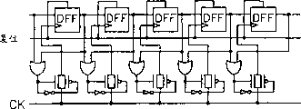
A static clock pulse generator comprises a plurality of stages 1,2, each of which comprises a D-type flip-flop 3 and a gating circuit 4. The flip-flop 3 supplies output signals Q of the stage which are also used as gating signals for the gating circuit 4 of the following stage. The gating circuit 4 supplies a signal to the data input D of the flip-flop 3 when its gating input G is active and a clock pulse is present on the clock input CK or ICK. An asynchronous reset signal R is supplied to the flip-flop 3 from the following stage.
Description
Technical field
The present invention relates to a kind of pulse generator for static clock.Such generator can be used for the controller circuitry of high-speed low-power-consumption, for example is used for comprising ultra-large integrated (VLSI) design of the complexity of Digital Signal Processing (DSP).Clock pulse generator can perform well in the addressing of the drive circuit of space light modulator and display, pixel (pixelated) matrix type for example, and wherein a series of clear and definite pulses must offer the circuit of sampling high-speed video data.
Background technology
A kind of clock pulse generator of known type is that the basis forms with the shift register.This shift register comprises in response to clock pulse so that the logic state of single storage is passed to Next level chain D flip-flop the link from a trigger, and is for example disclosed the same in Horowitz and Hill Cambridge University Press 1989 the 2nd edition " electronic technology ".For the application that typical clock pulse takes place, except one of them flip-flop states, all the other all flip-flop states all are predisposed to logic low (0) state, and this remaining trigger just is predisposed to logic high (1) state.Shift register is locked in known frequency place, and (circulating) 1 state that circulates in the shift register is used for producing sequential pulse at the output of trigger.The application of this known technology and embodiment for example are disclosed among the US 4,542,302 and US 4,612,659.A kind of improvement to this technology is disclosed in US4, in 785,297.In the case, " master " of edge-triggered D-flip flop and " from " output is used for and the compound logic door, as AND or the combination of NAND door, with the toggle speed of the shift register that reduces given output umber of pulse.
Accompanying drawing 1 expression comprises the part of the typical cmos circuit of D-type latch 1 and 2.The composition of this structure and operation principle are well-known, just do not describe in detail at this.The latch of Xiang Lianing is conspicuous as 1 and 2 on the opposite clock phase of the two phase clock of representing with CK and 1CK successively.The input of each latch and output can be produced clock pulse Nn and Np by NAND together.
In order to improve maximum operation frequency and to reduce the clock power consumption, the various technology that reduce the load of the clock line appearance of a street are disclosed.For example, State Control timing technology has been suggested and has been used for clock circuit.Such example is disclosed in US 4,746, and in 915, wherein shift register is divided into several sub-registers of trigger or latch, and another shift register with lower frequency work is used selectively clock signal is used for each sub-register.
For the application of single circulation 1 state of needs, only be that trigger or the latch that those inputs at them comprise one 1 states or have one 1 states needs timing.As shown in Figure 2, for such application, can be used in the clock signal that the control unlatching offers the trigger input end of clock by the input of " or operation " each trigger and the signal of output generation.Such structure has been disclosed in US 5,128, in 974.Yet such structure just needs more transistor at every grade.And the trigger output just must drive relatively large load, and this has just limited the maximal rate of operation.
Summary of the invention
Here employed term " D-type latch " is meant a kind of circuit input end of clock, data input pin and positive or reversed-phase output that has, this circuit is worked by this way: when the clock signal that promptly offers input end of clock is activated, this output provides the signal of a positive or anti-phase type at input (latch is " conspicuous "), and when clock signal is not activated, this output just be held or " locking " on its currency, and no matter the state of input end signal how.Here employed term " D flip-flop " is meant a kind ofly usually to be made up of the D-type latch of two level chains, also may comprise the edge-triggered equipment of adjunct circuit.D-type latch and D flip-flop are referred to as " D type circuit " here, and D type circuit can be a D-type latch or a D flip-flop like this.
According to the first string of the present invention, a kind of clock pulse generator that comprises a master clock input and N level is provided, each i level comprises: a D type circuit, it has one and is used for from the RESET input of (i+a) level reception reset signal, here a is more than or equal to 1 and one data input pin; One gating circuit, it has one and in response to the D type circuit output signal of (i-1) level and the clock pulse of master clock input one pulse is offered the output of data input pin, here 1<i≤(N-a).
Each D type circuit can be a D-type latch.
At least wherein each in the one-level can have one can provide D type circuit output signal and the output of forming generator output end.
The RESET input of the D type circuit of each i level can be arranged to receive the reset signal of (i+a) level gating circuit output.
The RESET input of the D type circuit of each i level can be arranged to receive the output end signal as the D type circuit of (i+a) level of reset signal.
Every grade can comprise one at every grade gating circuit output and the delay circuit between the D type circuit data input.Each delay circuit can comprise the inverter that several grades chain connects.
Every grade can comprise a switching device, it is used for connecting selectively D type circuit reset input to receive the reset signal of (i-a) level, with in response to (i+1) level D type circuit output signal and the clock pulse of master clock input make gating circuit that pulse is offered data input pin, wherein, (1+a)≤i<N.Each switching device can comprise several transmission gates.
The D type circuit of each i level can comprise a clock input, and it is used to receive the D type circuit output signal of (i-1) level.
This switching device can be arranged to connect selectively the D type circuit clock input of each i level, to receive the D type circuit output signal of (i+1) level.
The first order can comprise: a D type circuit, and it has a RESET input, is used to receive the reset signal and a data input pin of (1+a) level; One gating circuit, it is used for clock pulse in response to initial pulse and master clock input a pulse is offered D type circuit data input.
This switching device can be arranged to selectively the reset signal of the first order is connected with the RESET input of the D type circuit of the first order.
The N level comprises: a D type circuit, and it has a data input pin, and an output and is used to receive the RESET input of the reset signal of D type circuit output; With a gating circuit, it has one and is used for output in response to the D type circuit output signal of (N-1) level and the clock pulse of master clock input so that a pulse is offered data input pin.
The master clock input can comprise a complementary clock input, and several gating circuits to level of Xiang Lianing can be arranged to the complementary clock pulse in response to complementary input end successively.Each gating circuit can comprise a first transistor, and its public electrode is connected with the master clock input, and its output electrode forms a log-on data input of D type circuit, and its control electrode is in response to the output signal of the D type circuit of upper level.Each gating circuit can comprise a transistor seconds, and its public electrode is connected with one first power circuit, and its output electrode is connected with the output electrode of the first transistor.The control electrode of transistor seconds can be configured to receive the D type circuit output signal of upper level.
The control electrode of the first transistor can be connected with a bias voltage source, and this bias voltage source can be arranged to the D type circuit output signal control by upper level.This bias voltage source can comprise one the 3rd transistor, and its public electrode is connected with an anti-phase master clock input, and its control is connected with the control electrode of the first transistor with output electrode.The control electrode of the first transistor can be connected with the 4th transistorized output electrode, and the 4th transistorized public electrode is connected with first power circuit.The 4th transistorized control electrode can be configured to receive the D type circuit output signal of upper level.
The control electrode of the first transistor can be connected with the 5th transistorized output electrode, and the 5th transistorized public electrode is connected with a second source circuit, and its control electrode is arranged to receive the D type circuit output signal of upper level.
Each D-type latch can comprise one first inverter and one second feedback inverter.Second inverter can be a gated inverter, and it has the door input of being arranged to the D-type latch output signal control of upper level.
First inverter can be with one " height " conducting or " low " conduction pipe is connected, the control end of this conduction pipe comprises the RESET input.
This generator can form a CMOS integrated circuit.
This generator can be made by polysilicon transistors.
According to second scheme of the present invention, provide a kind of space light modulator that comprises the generator of the first string according to the present invention.
This modulator can comprise a liquid crystal apparatus.
This liquid crystal apparatus can be a passive matrix.
This liquid crystal apparatus can be an active array type.This generator and active matrix can be made by the thin-film transistor of same type.
According to the 3rd scheme of the present invention, provide a kind of display that comprises the modulator of second scheme according to the present invention.
According to the 4th scheme of the present invention, provide a kind of active display that comprises the generator of the first string according to the present invention.
This display can be passive or active array type.
Therefore, but the present invention can provide the clock pulse generator of a kind of high-speed cruising and low-power consumption.Such generator can provide the static state operation that does not have instantaneous walking circuit node and will hang down load and be added on the input clock signal.This generator can be arranged at an easy rate with the two-way mode operation, and can be made up of the transistor of relatively small amount.This generator can also move by the low-voltage input clock signal, can for example provide and from the clock signal to the output signal level, move, clock signal has 2v or littler value, and output signal can be switched between power circuit, and this power circuit can transmit the voltage of 10v to 20v usually.This performance realizes by using the polycrystalline SiTFT technology.
Description of drawings
The present invention is by being described in greater detail for example with reference to the accompanying drawings, wherein:
Fig. 1 is a kind of two-stage circuit figure of known type shift register;
Fig. 2 is a kind of circuit block diagram of known type clock pulse generator;
Fig. 3 is a kind of circuit diagram of two-stage of the pulse generator for static clock that constitutes the embodiment of the invention;
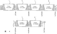
Fig. 4 is that progression is the block diagram of clock pulse generator as shown in Figure 3;
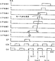
Fig. 5 is the chronogram of the waveform that produces in the clock pulse generator shown in Fig. 3 and 4;
Fig. 6 is the two-stage circuit figure that forms the pulse generator for static clock of one embodiment of the invention;
Fig. 7 is that progression is the block diagram of clock pulse generator as shown in Figure 6;
Fig. 8 is the chronogram of the waveform that produces in the clock pulse generator shown in Fig. 6 and 7;
Fig. 9 is the two-stage circuit figure that forms the pulse generator for static clock of one embodiment of the invention;
Figure 10 is that progression is the block diagram of clock pulse generator as shown in Figure 9;
Figure 11 is the chronogram of the waveform that produces in the clock pulse generator shown in Fig. 8 and 9;
Figure 12 is the two-stage circuit figure that forms the pulse generator for static clock of one embodiment of the invention;
Figure 13 is that progression is the block diagram of clock pulse generator as shown in figure 12;
Figure 14 is the chronogram of the waveform that produces in the clock pulse generator shown in Figure 12 and 13;
Figure 15 is the two-stage circuit figure that forms the pulse generator for static clock of one embodiment of the invention;
Figure 16 is the chronogram of the waveform that produces in clock pulse generator as shown in figure 15;
Figure 17 be form one embodiment of the invention the bidirectional static clock pulse generator the one-level circuit diagram and the work that it is two-way is described;
Figure 18 is an one-level circuit diagram of forming the pulse generator for static clock of one embodiment of the invention;
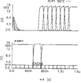
Figure 19 is the oscillogram that produces waveform in the analogue test of as shown in figure 18 clock pulse generator;
Figure 20 is an one-level circuit diagram of forming the pulse generator for static clock of one embodiment of the invention;
Figure 21 is an one-level circuit diagram of forming the pulse generator for static clock of one embodiment of the invention;
Figure 22 is an one-level circuit diagram of forming the bidirectional static clock pulse generator of one embodiment of the invention;
Figure 23 is a roughly block diagram of forming the display that comprises the liquid crystal spatial light line modulator of one embodiment of the invention.
All same reference number is represented identical parts in the accompanying drawing.
Embodiment
Fig. 3 represents the two- stage 1 and 2 of pulse generator for static clock.Level 1 comprises a D-type latch 3 and a gating circuit 4.Latch 3 have the positive that is connected with next stage and anti-phase output Q and! Q, output Q constitute the output of this grade and the output of clock pulse generator.This latch has the asynchronous reset inputs R of a reception next stage reset signal.
Fig. 4 represents to comprise the part pulse generator for static clock of the level 1,2 that N level chain connects.Level 1 is alternately changed with level 2.The complementary gating input G of the first order 1 and! G be arranged to receive complementary initial pulse SP and! SP, and input end of clock receive the two phase clock input complementary clock signal CK and! CK.The RESET input R of each level 1,2 is connected with the gating circuit output O of next stage (except afterbody or N level), and its RESET input R is connected with the output Q of peer.
The course of work of pulse generator for static clock explains with the chronogram of Fig. 5, and Fig. 5 is illustrated in the various waveforms that produce in first level Four of Fig. 4 generator.Originally, all latchs 3 of level 1 and 2 all are in reset mode so that all output Q are low level.All grades 1 and 2 gating circuit 4 quit work, and gating circuit output O is a low level.
At time t
nBefore, an initial pulse SP offers the gating circuit input of the first order.Therefore gating circuit 4 just can be activated, and the output O of gating circuit 4 can follow the logic state of clock signal C K, may move with the level of actual logic level.
At time t
nThe time, the rising edge that the output of gating circuit 4 is followed clock signal C K raises.Therefore the positive output end Q of latch 3 also rises, and starts the gating circuit 4 of next stage 2.
Only at time t
nAfter, initial pulse SP begins to descend so that the gating circuit of the first order quits work.The clock input CK of latch also descends, and Q is a high level state so that latch keeps its output, is received until reset signal.
At time t
N+1The time, the output O of the gating circuit 4 of the second level 2 follows the inversion clock signal! The rising edge of CK rises.The output Q of second level latch 3 also rises, and starts the gating circuit 4 of the third level.Simultaneously, the output O of partial gating circuit 4 provides the RESET input R of a reset signal to the latch of the first order, and therefore, its output Q descends.Therefore, the decline of the output Q of the level that links to each other successively and rising edge will take place simultaneously or synchronously, as shown in Figure 5.
At time t
N+2The time, the rising edge that the output O of the gating circuit 4 of the third level follows clock signal C K rises.Therefore the output Q of the third level also rises, and starts the gating circuit 4 of the fourth stage.Simultaneously, partial latch 3 is reset.The course of work is proceeded as mentioned above then, once and with the feedback signal of generator next stage resets once in the clock pulse of each latch 3 usefulness gating input set.
Fig. 8 represents the oscillogram that produces.Because each latch 3 just is reset after the latch 3 of next stage is set, all grades output Q is guaranteed by overlapping as shown in Figure 8.Therefore such structure is applicable to the clock pulse generator that requires to provide continuous overlapped signal.
As shown in figure 11, continuous output Q is at clock signal C K,! In the whole clock cycle of CK be activate or high level so that be simultaneous every trailing edge and the rising edge of an output Q.Consecutive numbers is overlapping with half clock cycle roughly to output end signal Q.
As shown in figure 16, the time-delay that is provided by every grade of delay circuit 5 guarantees that the latch 3 of upper level is being reset before latch 3 set of prime.This just guarantees in turn that the output Q of level is no longer overlapping continuously, may be required as the application of some clock pulse generators.
Figure 17 represent one be arranged to two-way operation promptly from left to right or from right to left order produce the level 1 of the type as shown in Figure 6 of pulse.Work is from left to right represented on the top of Figure 17 and work is from right to left represented in the bottom.The level 2 that inversion clock activates can be provided with in the same way.
Shown in the top of Figure 17, the composition of this generator is work from left to right, and switch 6 is connected the gating input G of gating circuit and the input end of clock CK of latch 3 with the terminal GR that receives upper level output signal Q.Switch 7 is connected the RESET input R of latch 3 with terminal RG, with the output Q that receives the next stage latch as reset signal.Therefore, this level just can be carried out work as mentioned above.
When the composition of this generator is from right to left work, switch 6 and 7 be connected shown in the bottom of Figure 17.The gating input G of gating circuit 4 and the input end of clock CK of latch 3 are connected with terminal RG, and receive the output Q of next stage latch.The RESET input R of latch 3 is connected with terminal GR, with the output Q that receives upper level latch 3 as reset signal.Therefore the pulse of this grade output Q can produce continuously from right to left.For the work of this pattern, the terminal of the first order and N level is connected can exchange so that the N level can receive initial pulse and the first order can self reset.
Figure 18 at length represented by the cmos fet pipe, for example is the example of the level 1 specialized of a kind of polycrystalline SiTFT form.Another level 2 also can be in the same way specialized, except with complementary clock circuit CK and! The exchange that CK connects.This structure can be carried out work by enough input clock voltage, and this input clock voltage roughly is lower than supply voltage, because 4 pairs of higher input clock signal level of gating circuit provide a kind of level locomotive function.In this structure, a gating circuit output! Q and latch the RESET input! R is " an activation low level ".
D-type latch 3 comprises a N transistor npn npn M5, P transistor npn npn M6 and M13, a single gate transistor M8 who is used for connecting, the three grid N transistor npn npns and of M10 and M12 be used for the connecting double grid P transistor npn npn of two single gate transistor M9 and M11.Transistor M5 and M6 form an inverter, the output of the input of this inverter and gating circuit 4! O is connected, and its output is formed the positive output end Q of level 1.Transistor M8-M12 forms a gating feedback inverter, its input and output respectively with inverter M5, the output of M6 is connected with input.
The grid of transistor M11 is connected with positive gating input G, and the grid of transistor M10 and anti-phase input! G is connected.Therefore, gating signal is when activating, and the inverter of gating just quits work, and at the gating input when not activating, the inverter of gating just can start work, and the output of locking latch.
Transistor M13 comprises one " height " conducting (pull-up) pipe, its source electrode and drain electrode respectively with the output of the first power circuit Vdd and gating circuit 4! O is connected.The RESET input is hanged down in the activation of the grid of transistor M13 and M12 and latch 3! R is connected.
The course of work of level 1 shown in Figure 180 is as described below.The gating input do not activate so as complementary strobe signals G and! When G was low level and high level respectively, transistor M2 and M4 just were cut off, " low " conducting (pull-down) transistor M7 guarantees that transistor M1 and M3 end.A so output of gating circuit 4! O is high-impedance state, not subject clock signal CK and! The influence of CK.A so output! O remains on logic high by the output of the inverter of gating, the state that it can locking latch 3.
Gating signal activate so as signal G and! When G was high level and low level respectively, the transistor M3 that two utmost points connect was as bias voltage source, and its load is provided by transistor M4.This bias voltage offers the grid of transistor M 1, and it plays a public gated amplifier, provides a load by transistor M2, at the gating circuit output! O provides a clock signal! The level of CK type moves pattern.Clock signal C K is a low level, the inversion clock signal! When CK was high level, grid-source voltage of transistor M1 was just lower, and transistor M2 keeps output! O approaches the positive voltage on the power circuit Vdd.On the contrary, clock signal C K and! When CK is high level and low level respectively, produce and offer the bias voltage of transistor M1 grid just than higher by transistor M3 and M4.Grid-source voltage of transistor M1 just raises to allow that transistor M1 makes output fully! O approaches the earth potential on the power circuit Vss.For this reason, the driving force of transistor M1 is greater than the driving force of transistor M2 basically.
D-type latch 3 with asynchronous reset is similar to D-type timing latch commonly used shown in Figure 1, but it has the first order timing inverter of part gating circuit 4 so that the output of gating circuit! A complementary output end of O and latch 3! Q has identical node.Transistor M3 is by making node! Q rises to high level so that asynchronous reset to be provided, and output Q just becomes low level like this, and transistor M2 prevents any transistor conflict that produces when resetting.
As mentioned above, when gating input G is low level, the locking mechanism of latch 3 be activated so as output Q and! Q keeps locking under its current logical value.Therefore, because gating circuit 4 does not activate, latch just has been determined the gating circuit output! Voltage on the O.Yet, " height " conduction pipe M13 still can reset latch.
On the contrary, when gating input G was high level, the locking mechanism of latch 3 just quit work, and gating circuit 4 just is activated.Therefore, gating circuit 4 just has been determined output! The logic state of O, therefore and determined the logic level of latch 3 output Q.
Voltage waveform shown in Figure 19 comes from the transient analysis simulation drawing that comprises clock pulse generator type level shown in Figure 180, that have the 15v supply voltage.Transistor is with the characteristic of typical low-temperature polysilicon film transistor, and promptly rectangular apparatus has threshold voltage and the 1.25 μ A/V of 2v
2Mutual conductance simulated.The clock input is the complementary signal of 2v magnitude of voltage and 5MHz.
The oscillogram of Figure 19 bottom is represented clock and initial pulse, and upper waveform figure represents the clock pulse generator output signal of level continuously.Therefore, after initial pulse, clock pulse generator produces gratifying output pulse, and its amplitude roughly equates with supply voltage.This can utilize the level of exporting pulse from the 2v clock pulse to 15v to move and realize.
Figure 20 represents that one is different from clock pulse generator level 1 shown in Figure 180, and its difference is that feedback inverter is non-gate type, i.e. " transistor " M10, and M11 and M12 have been omitted.For this structure is correctly worked, transistor M8 compares with M13 with transistor M1 with M9 must have lower driving force.Yet this just provides fairly simple circuit structure, and positive gating circuit G just can be omitted.Similarly, if do not need to provide level output, positive output end Q also can omit.
Figure 21 has represented to omit the fairly simple circuit structure of transistor M2 of the level of Figure 20.In course of normal operation, an output of gating circuit 4! O keeps high level by transistor M9.Yet when gating circuit 4 was activated, transistor M9 was used as the load of transistor M1 and keeps output! The high level of O is until the rising edge of positive clock pulse CK.Transistor M1 makes output then! O reduces to low level, and transistor M13 makes output! O roughly lags behind and rises after half clock cycle.
Figure 22 represents to have shown in Figure 180 grade two-way embodiment of construction of switch, and this construction of switch is formed by the transmission gate circuit setting that comprises transistor M14-M22.The control input end of transmission gate circuit and a complementary left side/right control circuit LR with! LR is connected, like this, when needs carry out left-to-right work, control signal LR and! LR will be respectively high level and low level, and when needs carry out right work to a left side, control signal LR and! LR will be respectively low level and high level.Inverter I1 is from by anti-phase gating signal for fear of bidirectional operation being changed positive gating signal G respectively! G produces positive gating signal G.
Figure 23 represent to comprise a N capable * display of M row pixel display matrix 40, for example be a kind of space light modulator form that comprises LCD.This display comprises that also one has the address signal generator 41 of clock circuit 42 and one group of data circuit driver 43.This clock circuit 42 comprises shown in Fig. 3 to 22 and the generator of foregoing arbitrary type.One scan signal generator 44 offers the row of pixel with sweep signal, and it comprises a clock circuit 45 and one group of line driver 46.This clock circuit 45 comprises shown in Fig. 3 to 22 and the generator of foregoing arbitrary type.This clock circuit produces clock pulse with the pixel data rate of circuit 42 and the track data rate of circuit 45.
Claims (37)
1. pulse generator for static clock that comprises a master clock input and N level, each i level comprises: a D type circuit, it has a RESET input that is used to receive i+a level reset signal, and a is more than or equal to 1 and one data input pin here; One gating circuit, it has one in response to the clock pulse of the D type circuit output signal of i-1 level and master clock input and a pulse is offered the output of data input pin, 1<i≤N-a, wherein N>a+1 here.
2. generator as claimed in claim 1 is characterized in that: each D type circuit is a D-type latch.
3. generator as claimed in claim 1 is characterized in that: each one-level wherein has one at least can provide D type circuit output signal and the output of forming generator output end.
4. generator as claimed in claim 1 is characterized in that: the RESET input of the D type circuit of each i level is arranged to receive the reset signal of i+a level gating circuit output.
5. generator as claimed in claim 1 is characterized in that: the RESET input of the D type circuit of each i level is arranged to receive the output end signal as the D type circuit of the i+a level of reset signal.
6. generator as claimed in claim 1 is characterized in that: every grade comprises a delay circuit between every grade of gating circuit output and D type circuit data input.
7. generator as claimed in claim 6 is characterized in that: each delay circuit comprises the inverter that several grades chain connects.
8. generator as claimed in claim 1, it is characterized in that: every grade comprises a switching device, it is used for connecting selectively D type circuit reset input to receive the reset signal of i-a level, with make gating circuit in response to the clock pulse of the D type circuit output signal of i+1 level and master clock input pulse is offered data input pin, wherein, 1+a≤i<N.
9. generator as claimed in claim 8 is characterized in that: each switching device comprises several transmission gate circuits.
10. generator as claimed in claim 1 is characterized in that: the D type circuit of each i level comprises a clock input, and it is used to receive the output signal of the D type circuit of i-1 level.
11. generator as claimed in claim 8 is characterized in that: the D type circuit clock input that this switching device is arranged to connect selectively each i level is with the output signal of the D type circuit that receives the i+1 level.
12. generator as claimed in claim 1 is characterized in that: the first order comprises: a D type circuit, it has a RESET input, is used to receive the reset signal and a data input pin of 1+a level; One gating circuit, it is used for clock pulse in response to initial pulse and master clock input a pulse is offered D type circuit data input.
13. generator as claimed in claim 8 is characterized in that: this switching device is arranged to selectively the reset signal of the first order is connected with the RESET input of the D type circuit of the first order.
14. generator as claimed in claim 1 is characterized in that: the N level comprises: a D type circuit, it has a data input pin, and an output and is used to receive the RESET input of D type circuit output reset signal; One gating circuit, it have one in response to the clock pulse of the D type circuit output signal of N-1 level and master clock input a pulse is offered the output of data input pin.
15. generator as claimed in claim 1 is characterized in that: the master clock input comprises a complementary clock input, and several gating circuits to level of Xiang Lianing are arranged to the complementary clock pulse in response to complementary input end successively.
16. generator as claimed in claim 1, it is characterized in that: each gating circuit comprises a first transistor, its public electrode is connected with the master clock input, its output electrode forms a log-on data input of D type circuit, and its control electrode is corresponding to the output signal of the D type circuit of upper level.
17. generator as claimed in claim 16 is characterized in that: each gating circuit comprises a transistor seconds, and its public electrode is connected with one first power circuit, and its output electrode is connected with the output electrode of the first transistor.
18. generator as claimed in claim 17 is characterized in that: the control electrode of transistor seconds is configured to receive the D type circuit output signal of upper level.
19. generator as claimed in claim 16 is characterized in that: the control electrode of the first transistor is connected with a bias voltage source, and this bias voltage source is arranged to the D type circuit output signal control by upper level.
20. generator as claimed in claim 19 is characterized in that: this bias voltage source comprises one the 3rd transistor, and its public electrode is connected with an anti-phase master clock input, and its control is connected with the control electrode of the first transistor with output electrode.
21. generator as claimed in claim 20 is characterized in that: the control electrode of the first transistor is connected with one the 4th transistorized output electrode, and the 4th transistorized public electrode is connected with first power circuit.
22. generator as claimed in claim 21 is characterized in that: the 4th transistorized control electrode is configured to receive the output signal of upper level D type circuit.
23. generator as claimed in claim 16, it is characterized in that: the control electrode of the first transistor is connected with the 5th transistorized output electrode, the 5th transistorized public electrode is connected with a second source circuit, and its control electrode is arranged to receive the output signal of upper level D type circuit.
24. generator as claimed in claim 2 is characterized in that: each D-type latch comprises one first inverter and one second feedback inverter.
25. generator as claimed in claim 24 is characterized in that: second inverter is a gated inverter, and it has the door input of being arranged to the control of upper level D-type latch output signal.
26. generator as claimed in claim 24 is characterized in that: first inverter and a control end comprise the RESET input " height " conducting or " low " conduction pipe is connected.
27. generator as claimed in claim 1 is characterized in that: this generator forms a CMOS integrated circuit.
28. generator as claimed in claim 1 is characterized in that: this generator is made by polycrystalline SiTFT.
29. a space light modulator, it comprises generator as claimed in claim 1.
30. modulator as claimed in claim 29 is characterized in that: it comprises a liquid crystal apparatus.
31. modulator as claimed in claim 30 is characterized in that: this liquid crystal apparatus is a passive matrix.
32. modulator as claimed in claim 30 is characterized in that: this liquid crystal apparatus is an active array type.
33. modulator as claimed in claim 32 is characterized in that: this generator and active matrix are made by the thin-film transistor of same type.
34. a display, it comprises modulator as claimed in claim 29.
35. an active display, it comprises generator as claimed in claim 1.
36. the display of a passive matrix, comprise a pulse generator for static clock, described pulse generator for static clock comprises a master clock input and has N level, each i level comprises: a D type circuit, it has a RESET input that is used to receive i+a level reset signal, here a is more than or equal to 1 and one data input pin; One gating circuit, it has one in response to the clock pulse of the D type circuit output signal of i-1 level and master clock input and a pulse is offered the output of data input pin, 1<i≤N-a, wherein N>a+1 here.
37. the display of an active array type, comprise a pulse generator for static clock, described pulse generator for static clock comprises a master clock input and has N level, each i level comprises: a D type circuit, it has a RESET input that is used to receive i+a level reset signal, here a is more than or equal to 1 and one data input pin; One gating circuit, it has one in response to the clock pulse of the D type circuit output signal of i-1 level and master clock input and a pulse is offered the output of data input pin, 1<i≤N-a, wherein N>a+1 here.
Applications Claiming Priority (2)
| Application Number | Priority Date | Filing Date | Title |
|---|---|---|---|
| GB0008080A GB2361121A (en) | 2000-04-04 | 2000-04-04 | A CMOS LCD scan pulse generating chain comprising static latches |
| GB0008080.4 | 2000-04-04 |
Publications (2)
| Publication Number | Publication Date |
|---|---|
| CN1332520A CN1332520A (en) | 2002-01-23 |
| CN1238970C true CN1238970C (en) | 2006-01-25 |
Family
ID=9889034
Family Applications (1)
| Application Number | Title | Priority Date | Filing Date |
|---|---|---|---|
| CNB011178965A Expired - Fee Related CN1238970C (en) | 2000-04-04 | 2001-04-04 | Pulse generator for static clock |
Country Status (6)
| Country | Link |
|---|---|
| US (1) | US6377104B2 (en) |
| JP (2) | JP2001356728A (en) |
| KR (1) | KR100375907B1 (en) |
| CN (1) | CN1238970C (en) |
| GB (1) | GB2361121A (en) |
| TW (1) | TW508549B (en) |
Families Citing this family (21)
| Publication number | Priority date | Publication date | Assignee | Title |
|---|---|---|---|---|
| GB2397710A (en) * | 2003-01-25 | 2004-07-28 | Sharp Kk | A shift register for an LCD driver, comprising reset-dominant RS flip-flops |
| JP4265934B2 (en) * | 2003-06-06 | 2009-05-20 | シャープ株式会社 | Scan campus circuit, logic circuit including the same, and integrated circuit test method |
| JP3974124B2 (en) * | 2003-07-09 | 2007-09-12 | シャープ株式会社 | Shift register and display device using the same |
| KR100557636B1 (en) * | 2003-12-23 | 2006-03-10 | 주식회사 하이닉스반도체 | Data strobe circuit using clk signal |
| JP3958322B2 (en) * | 2004-01-28 | 2007-08-15 | シャープ株式会社 | Shift register and active matrix display device |
| JP4625841B2 (en) * | 2004-06-14 | 2011-02-02 | ザ・ユニバーシティ・オブ・ノース・カロライナ・アット・グリーンズボロ | System and method for digital content security |
| US8098225B2 (en) * | 2004-10-14 | 2012-01-17 | Sharp Kabushiki Kaisha | Display device driving circuit and display device including same |
| KR101074424B1 (en) * | 2004-11-05 | 2011-10-17 | 삼성전자주식회사 | High-speed low-power clock gated logic circuit |
| US7131092B2 (en) * | 2004-12-21 | 2006-10-31 | Via Technologies, Inc. | Clock gating circuit |
| CN101223606B (en) * | 2005-07-15 | 2012-09-05 | 夏普株式会社 | Signal output circuit, shift register, output signal generation method, display device drive circuit, and display device |
| KR100624115B1 (en) * | 2005-08-16 | 2006-09-15 | 삼성에스디아이 주식회사 | Emission driver of being uses in organic electroluminescence display device |
| US8396112B2 (en) | 2006-11-28 | 2013-03-12 | Seiko Epson Corporation | Circuitry and method for transferring data, and circuitry and method utilizing clock pulses |
| US20080304664A1 (en) * | 2007-06-07 | 2008-12-11 | Shanmugathasan Suthaharan | System and a method for securing information |
| EP2447951B1 (en) * | 2009-06-17 | 2015-03-04 | Sharp Kabushiki Kaisha | Flip-flop, shift register, display drive circuit, display apparatus, and display panel |
| US8957843B2 (en) | 2010-02-25 | 2015-02-17 | Samsung Display Co., Ltd. | Gate selection circuit of liquid crystal panel, accumulating capacity driving circuit, driving device, and driving method |
| CN104658508B (en) * | 2015-03-24 | 2017-06-09 | 京东方科技集团股份有限公司 | A kind of shift register cell, gate driving circuit and display device |
| CN104835443B (en) * | 2015-06-03 | 2017-09-26 | 京东方科技集团股份有限公司 | A kind of shifting deposit unit, gate driving circuit and display device |
| CN106683634B (en) * | 2017-03-30 | 2019-01-22 | 京东方科技集团股份有限公司 | A kind of shift register, GOA circuit and its driving method, display device |
| CN114629470A (en) * | 2022-02-16 | 2022-06-14 | 北京大学 | High-speed pulse generator and high-speed pulse generating method |
| TWI816348B (en) * | 2022-03-31 | 2023-09-21 | 友達光電股份有限公司 | Data driver and control method |
| CN115021720A (en) * | 2022-05-13 | 2022-09-06 | 北京大学 | Width-adjustable high-speed pulse generator circuit and high-speed pulse generation method |
Family Cites Families (18)
| Publication number | Priority date | Publication date | Assignee | Title |
|---|---|---|---|---|
| SE408985B (en) * | 1977-12-27 | 1979-07-16 | Philips Svenska Ab | PULSE GENERATOR |
| JPS6066396A (en) * | 1983-09-20 | 1985-04-16 | Fujitsu Ltd | Shift register |
| US4641102A (en) * | 1984-08-17 | 1987-02-03 | At&T Bell Laboratories | Random number generator |
| US4691122A (en) * | 1985-03-29 | 1987-09-01 | Advanced Micro Devices, Inc. | CMOS D-type flip-flop circuits |
| JPH03147598A (en) * | 1989-11-02 | 1991-06-24 | Sony Corp | Shift register |
| US5105187A (en) * | 1990-04-18 | 1992-04-14 | General Electric Company | Shift register for active matrix display devices |
| US5140180A (en) * | 1990-08-24 | 1992-08-18 | Ncr Corporation | High speed cmos flip-flop employing clocked tristate inverters |
| KR930022729A (en) * | 1992-04-08 | 1993-11-24 | 김광호 | 2 times operating frequency regeneration circuit |
| JPH06204809A (en) * | 1992-12-30 | 1994-07-22 | Sony Corp | Ring oscillator |
| JPH07248741A (en) * | 1994-03-09 | 1995-09-26 | New Japan Radio Co Ltd | Data shift circuit |
| US5451911A (en) * | 1994-04-07 | 1995-09-19 | Media Vision, Inc. | Timing generator |
| JP3146959B2 (en) * | 1995-11-30 | 2001-03-19 | 松下電器産業株式会社 | Liquid crystal display device and shift register circuit thereof |
| JP3516323B2 (en) * | 1996-05-23 | 2004-04-05 | シャープ株式会社 | Shift register circuit and image display device |
| US6040812A (en) * | 1996-06-19 | 2000-03-21 | Xerox Corporation | Active matrix display with integrated drive circuitry |
| GB2345207A (en) * | 1998-12-22 | 2000-06-28 | Sharp Kk | Static clock pulse generator for LCD |
| JP3588020B2 (en) * | 1999-11-01 | 2004-11-10 | シャープ株式会社 | Shift register and image display device |
| JP3588033B2 (en) * | 2000-04-18 | 2004-11-10 | シャープ株式会社 | Shift register and image display device having the same |
| JP3535067B2 (en) * | 2000-03-16 | 2004-06-07 | シャープ株式会社 | Liquid crystal display |
-
2000
- 2000-04-04 GB GB0008080A patent/GB2361121A/en not_active Withdrawn
-
2001
- 2001-03-28 US US09/819,944 patent/US6377104B2/en not_active Expired - Lifetime
- 2001-03-29 JP JP2001097404A patent/JP2001356728A/en active Pending
- 2001-04-04 CN CNB011178965A patent/CN1238970C/en not_active Expired - Fee Related
- 2001-04-04 KR KR10-2001-0017989A patent/KR100375907B1/en not_active IP Right Cessation
- 2001-04-04 TW TW090108138A patent/TW508549B/en not_active IP Right Cessation
-
2006
- 2006-04-10 JP JP2006108073A patent/JP4737627B2/en not_active Expired - Fee Related
Also Published As
| Publication number | Publication date |
|---|---|
| JP2001356728A (en) | 2001-12-26 |
| KR20010095330A (en) | 2001-11-03 |
| JP4737627B2 (en) | 2011-08-03 |
| KR100375907B1 (en) | 2003-03-15 |
| US6377104B2 (en) | 2002-04-23 |
| TW508549B (en) | 2002-11-01 |
| US20010043496A1 (en) | 2001-11-22 |
| CN1332520A (en) | 2002-01-23 |
| JP2006259753A (en) | 2006-09-28 |
| GB0008080D0 (en) | 2000-05-24 |
| GB2361121A (en) | 2001-10-10 |
Similar Documents
| Publication | Publication Date | Title |
|---|---|---|
| CN1238970C (en) | Pulse generator for static clock | |
| CN1296882C (en) | Bidirectional driving circuit of plate display equipment and its driving method | |
| CN1609939A (en) | Shift register | |
| CN1109405C (en) | Output buffer circuit having low breakdown voltage | |
| CN104978943B (en) | A kind of shift register, the driving method of display floater and relevant apparatus | |
| CN1428759A (en) | Shift register with built-in level shifter | |
| CN1258150C (en) | Semiconductor device | |
| CN103617775B (en) | Shift register cell, gate driver circuit and display | |
| CN1523553A (en) | Gate driver for a display device | |
| CN105741744A (en) | Shifting register unit, grid driving circuit and display device | |
| US11307707B2 (en) | Scan shift circuit, touch shift circuit, driving method and related apparatus | |
| CN101978428A (en) | Shift register and active matrix device | |
| CN1585271A (en) | Semiconductor integrated circuit | |
| CN1212435A (en) | Semiconductor integrated circuit having tri-state logie gate circuit | |
| KR20130023488A (en) | Scan driver and organic light emitting display device using thereof | |
| CN1260888C (en) | Level drift circuit and active matrix driver | |
| CN1917089A (en) | Dynamic shift reister and its inhibition circuit | |
| CN1870430A (en) | Duty cycle corrector | |
| CN1694358A (en) | Level shifter and panel display using the same | |
| KR20020088400A (en) | Signal processing circuit, low-voltage signal generator and image display incorporation the same | |
| CN100433090C (en) | Semiconductor integrated circuit device | |
| CN1236558C (en) | Pulse signal transforming delay regulating circuit | |
| CN106328034B (en) | Touch-control shift register, its driving method, touch drive circuit and relevant apparatus | |
| CN103050104B (en) | Decoding scanning driving device | |
| CN1921017A (en) | Shift register, scanning line driving circuit, matrix type device, electro-optic device, and electronic device |
Legal Events
| Date | Code | Title | Description |
|---|---|---|---|
| C10 | Entry into substantive examination | ||
| SE01 | Entry into force of request for substantive examination | ||
| C06 | Publication | ||
| PB01 | Publication | ||
| C14 | Grant of patent or utility model | ||
| GR01 | Patent grant | ||
| CF01 | Termination of patent right due to non-payment of annual fee | ||
| CF01 | Termination of patent right due to non-payment of annual fee |
Granted publication date: 20060125 Termination date: 20160404 |