CN1231545A - Matched filter bank - Google Patents
Matched filter bank Download PDFInfo
- Publication number
- CN1231545A CN1231545A CN99102307A CN99102307A CN1231545A CN 1231545 A CN1231545 A CN 1231545A CN 99102307 A CN99102307 A CN 99102307A CN 99102307 A CN99102307 A CN 99102307A CN 1231545 A CN1231545 A CN 1231545A
- Authority
- CN
- China
- Prior art keywords
- input
- output
- register
- sampling
- matched filter
- Prior art date
- Legal status (The legal status is an assumption and is not a legal conclusion. Google has not performed a legal analysis and makes no representation as to the accuracy of the status listed.)
- Pending
Links
Images


Classifications
-
- H—ELECTRICITY
- H04—ELECTRIC COMMUNICATION TECHNIQUE
- H04B—TRANSMISSION
- H04B7/00—Radio transmission systems, i.e. using radiation field
- H04B7/14—Relay systems
- H04B7/15—Active relay systems
- H04B7/204—Multiple access
- H04B7/216—Code division or spread-spectrum multiple access [CDMA, SSMA]
-
- H—ELECTRICITY
- H04—ELECTRIC COMMUNICATION TECHNIQUE
- H04B—TRANSMISSION
- H04B1/00—Details of transmission systems, not covered by a single one of groups H04B3/00 - H04B13/00; Details of transmission systems not characterised by the medium used for transmission
- H04B1/69—Spread spectrum techniques
- H04B1/707—Spread spectrum techniques using direct sequence modulation
- H04B1/709—Correlator structure
- H04B1/7093—Matched filter type
-
- H—ELECTRICITY
- H04—ELECTRIC COMMUNICATION TECHNIQUE
- H04B—TRANSMISSION
- H04B2201/00—Indexing scheme relating to details of transmission systems not covered by a single group of H04B3/00 - H04B13/00
- H04B2201/69—Orthogonal indexing scheme relating to spread spectrum techniques in general
- H04B2201/707—Orthogonal indexing scheme relating to spread spectrum techniques in general relating to direct sequence modulation
- H04B2201/70707—Efficiency-related aspects
Abstract
A matched filter bank including a plurality of matched filters and a sampling and holding units commonly used by the total matched filters. An inverting amplifier for the matched filter with a variable gain includes an input capacitance, an inverting amplifier connected to an output of the input capacitance, and a plurality of feedback capacitances connected between an input and output of the inverting amplifier. A plurality of switches are connected to input side of the feedback capacitances for alternatively connecting the feedback capcitanec to the input of the inverting amplifier or a reference voltage. The feedback capacitances connected to the reference voltage are invalid with respect to a composite capacitance of the feedback capacitance and have no influence to the amplifier.
Description
The present invention relates to matched filter banks, relate to the matched filter banks of the signal receiving device that is used for the DS-CDMA cellular system in particular.
Recently, because the capacity of direct sequence CDMA (DS-CDMA) system is very big, so along with the increase of land mobile number of users, the DS-CDMA system more and more is subjected to people's attention.In the DS-CDMA system, in sender side, these transmission data are modulated, expanded by a PN pseudo random sequence code then, and at receiver-side, this received signal is carried out de-spread with this PN pseudo random sequence code, with the regenerative transmission data.Use a sliding correlation detector or a matched filter during de-spread.The circuit size of sliding correlation detector is little, but needs long time to carry out correlation computations.And the speed of matched filter when carrying out correlation computations is fast, and its circuit size is but bigger comparatively speaking.
Traditional matched filter comprises a charge coupled device (CCD), a surface acoustic wave (SAW) device, perhaps a digital circuit.Inventor of the present invention has proposed a matched filter in patent publication No. Hei06-164320, this matched filter comprises an analog circuit, and its speed height and power consumption are low.This matched filter comprises sampling and the holding circuit that keeps a plurality of input analog signals as discrete data, a plurality of mlultiplying circuits with by multiplier the analog signal that is shifted and circulate is multiplied each other and one all product data are added together adder.
Recently, need to transmit the mutually different signal of multiple its transmission rate in the multimedia communication.So, just changed expansion ratio (variable expansion ratio system), perhaps walk abreast and used two or more extended code (many code systems).For these systems, just need have a plurality of matched filters of different number of taps.This makes the size of circuit become big, and power consumption has been increased.
The above-mentioned analog type matched filter that inventor of the present invention proposed has used an inverting amplifier as shown in Figure 12.This inverting amplifier comprises that has amplifier AMP high-gain, that comprise odd number series connection CMOS inverter.The input of this amplifier AMP links to each other with CI2 with a plurality of input capacitance CI1.Between the input and output of this amplifier AMP, be connected with a plurality of feedback capacity Cf1 to Cf6.These feedback capacities Cf1 to Cf6 links to each other with the output of this amplifier AMP by the switch MUX1 to MUX6 that makes these feedback capacities and link to each other with the output of this amplifier or link to each other with a reference voltage Vref.For example, these capacitor C f1, Cf2, Cf3, Cf4, the capacitance of Cf5 and Cf6 is proportional to 2 respectively
0, 2
1, 2
2, 2
3, 2
4, 2
5So, the combination capacitor that can obtain to have various values by control switch MUX1 to MUX6.Control signal S1 to S6 controls these switches MUX1 to MUX6 by the logic sum gate G1 to G6 of a refresh signal REF of further reception.Control signal S1 to S6 is being input to later on or door through anti-phase.When or the output of door when being high level, the output of these or door is low level, these feedback capacities link to each other with the output of amplifier AMP then.When REF is high level or control signal when being low level, these feedback capacities link to each other with this reference voltage then.The input of input capacitance CI1 and CI2 links to each other with an input refresh switch MUXR1, and an amplifier refresh switch SWR is connected between the input and output of amplifier AMP.Control these switches MUXR1 and SWR by refresh signal REF.When refreshing, the input and output of this amplifier AMP are by short circuit, and capacitor C I1 links to each other with this reference voltage with capacitor C I2.
When being one, this amplifier of supposition AMP has infinitely great gain, the desirable amplifier of performance, the input of this amplifier is Vref, input voltage is voltage VI1 and the VI2 on capacitor C I1 and the CI2, and the output of this amplifier is Vo, then carries out the weighted addition in the following formula (1).
In the amplifier of a reality, input voltage is not Vref, and its gain also is limited.When gain was A, total effectively feedback capacity was CVf, and total non-effective feedback capacity is CIf, and output voltage V o1 represents with following formula (2).
From formula (2) as can be seen, the error of output mainly is the influence that is subjected to limited gain-bandwidth (GB) product.When the capacitance of capacitor C If increased, it is bigger that this error just becomes.
An object of the present invention is to provide a matched filter banks, can not only reduce power consumption, can also reduce circuit size with a plurality of expansion ratios.
Another object of the present invention is for a matched filter provides an inverting amplifier circuit, and this inverting amplifier is simple, and its accuracy is high and reaction is quick.
A matched filter banks according to the present invention has one by common sampling and the holding circuit of using of a plurality of matched filters.
An inverting amplifier circuit according to the present invention comprises that a plurality of bag feeds hold, and their input links to each other with the input of an amplifier or link to each other with a reference voltage, to control the combination of effective feedback capacity.Invalid feedback capacity does not link to each other with the input of amplifier.
Fig. 1 is the block diagram of explanation according to first execution mode of a matched filter banks of the present invention;
Fig. 2 is the block diagram of explanation according to second execution mode of a matched filter banks of the present invention;
Fig. 3 be explanation in first execution mode sampling and a block diagram of holding circuit;
Fig. 4 is a block diagram of a PN register in explanation first execution mode;
Fig. 5 is a block diagram of its PN register of linking to each other with another multiplier of input of explanation;
Fig. 6 is a block diagram of a mask register of explanation and an input register;
Fig. 7 is a block diagram of the variation of a mask register of explanation;
Fig. 8 is a block diagram of the 3rd execution mode of a matched filter of explanation;
Fig. 9 is the block diagram that explanation has an inverting amplifier of a variable gain;
Figure 10 is the block diagram of explanation according to a scalar circuit of the present invention;
Figure 11 is a figure, and it compares the output characteristic of the circuit of Fig. 9 and the output characteristic of a circuit common;
Figure 12 is the individual circuit diagram with conventional inverter amplifier of variable gain of explanation; With
Figure 13 is an equivalent electric circuit of an actual amplifier.
Fig. 1 is the block diagram of explanation according to first execution mode of a matched filter banks of the present invention.In this matched filter banks, the input signal sampling that is shifted by a PN sign indicating number sequence is not shifted and circulates.This matched filter banks can be used for the coefficient to any length, for example is used for the PN sign indicating number sequence of de-spread, carries out related operation.This matched filter banks can comprise the matched filter of any number.In this embodiment, have two kinds of length to be respectively the PN sign indicating number sequence of 4 chips and 256 chips, and have two kinds respectively with these two kinds of corresponding matched filters of PN sign indicating number sequence.
In Fig. 1,11 is input end of analog signal that receive a baseband signal that produces by an antenna from a received signal.12 is a sampling and holding unit, comprises sampling and holding circuit SH1 to SH256 that a plurality of whiles link to each other with input end of analog signal.This sampling and holding circuit respond to a control signal that is shown as " 1 " and " 0 " on unit 12, receive this input signal, when this control signal is " 1 ", are used for sampling and maintenance.Each sampling clock CL, this control signal is just by towards dextroposition once.
At first, this control signal that is used for first order sampling and holding circuit SH1 is " 1 ", so that kept by SH1 from this analog input signal of holding 11 inputs.At next sampling time point, this control signal that is used for second level sampling and holding circuit SH2 is " 1 ", and other control signals are " 0 ".Like this, second level sampling and holding circuit SH2 receive this input signal.Then, this input signal is sampled and holding circuit SH3, SH4 ... following a ground for one receives.Sampling in the end and holding circuit SH256 have received after this analog input signal, and sampling is again from first order sampling and holding circuit SH1.
13 is one the one PN sign indicating number registers, in this embodiment, has preserved 256 chips of a PN sign indicating number sequence (PN1 to PN256).This PN sign indicating number register is a circulating register, and it is to responding circulating shift data with the synchronous shift clock CL1 of sampling clock CL.Each sampling time interval, these data just are shifted once.14
1To 14
256Be a mlultiplying circuit, output that it will come from all grades of PN sign indicating number register 13 and output multiplication from all samplings and holding circuit SH1 to SH256.
Because be kept at 256 the chip data numerical data normally in this PN sign indicating number register 13, so mlultiplying circuit 14
1To 14
256Be an analog to digital mlultiplying circuit, wherein each mlultiplying circuit multiply by a numerical data with this analog input signal.Inventor of the present invention has recommended this analog to digital mlultiplying circuit.
The 15th, to 14
1To 14
256An analog adder of addition is carried out in the output of mlultiplying circuit.The relevant output of sampling with 256 received signals in the PN sign indicating number sequence in the PN sign indicating number register 13 and sampling and the holding unit 12 with 256 chips.From power consumption and calculating order of accuarcy, this analog to digital mlultiplying circuit that inventor of the present invention proposed has advantage.
After starting working, be sampled to the analog input signal of input 11 and continue sampling with holding circuit SH1 to SH256 and be held.When 256 sampling clocks are imported into sampling and during holding unit 12,256 signal samplings have been full of among total 256 samplings and the holding circuit SH1 to SH256.In this time, mlultiplying circuit 14
1To 14
256To multiply by PN sign indicating number PN1 to PN256 in the sampling (S1 to S256) among sampling and the holding circuit SH1 to SH256, and calculate (PN1 * S1+PN2 * S2+ ... the summation of+PN256 * S256).
When the pulse of the 257th sampling clock was imported into sampling and holding unit 12, the oldest data were substituted by a new sampling S257 in sampling and holding circuit SH1.When the sampling S257 new to this sampled, a shift clock CL1 was imported into PN sign indicating number register 13, so that PN sign indicating number register 13 is with sign indicating number right shift one-level.Then, PN256 is maintained at the first order, and PN1 is maintained at the second level, and PN2 is maintained at the third level, and usually, PNi (i<255) is maintained at (i+1) level.Adder 15 outputs,
(PN256×S257+PN1×S2+…+PN255×S256)。
After, sampling and holding circuit SH2 to SH256 constantly press sampling clock CL input to analog input signal, a then ground sampling, and synchronous with the carrying out of sampling, the PN sign indicating number in the PN sign indicating number register 13 carries out cyclic shift by shift clock CL1.This input analog signal sampling is exported from adder 15 continuously with the correlated results of PN sign indicating number sequence.
16 is the 2nd PN sign indicating number registers that comprise 256 grades, and its life cycle is that the one-period PN sign indicating number sequence of 4 chips is calculated relevant.The PN sign indicating number sequence of one 4 chip (PN ' 1 is to PN ' 4) repeatedly is kept in the PN sign indicating number register 16.This PN sign indicating number sequence PN ' 1 to PN ' 4 is stored in first to fourth grade, and is stored in the 5th to the 8th grade.Similarly, four chip PN sign indicating number sequences are stored in the 8th grade of each later level Four.One second shift clock CL2 inputs in this second register, and this second register pair PN carries out right shift and circulates this PN sign indicating number.This second shift clock CL2 is identical with the first shift clock CL1.
17
1To 17
256It is the analog to digital mlultiplying circuit that PN sign indicating number in the PN sign indicating number register 16 and the input signal sampling that is kept in the sample holding unit 12 are multiplied each other.
The 18th, 256 grades of cyclical patterns mask registers as shown in Figure 1." 1 " is kept in the continuous level Four of mask register 18, and " 0 " is kept in other levels.These data right shifts.In this embodiment, " 1 " is stored in the 253rd to the 256th grade, and " 0 " is stored in the 1st to the 252nd grade.When the number of times that is input to register 18 as shift clock CL2 was 4 times, " 1 " was moved to the first order to the fourth stage, and other levels are " 0 ".
The output that mask register is 18 grades is used as control signal and is input to multiplexer MUX20
1To 20
256
19 is the permanent inputs for " 0 " of input, so that " 0 " is input to an analog adder 21.Multiplexer MUX20
1To 20
256Control signal to mask register 18 responds, and optionally exports mlultiplying circuit 17
1To 17
256Output and by end " 0 " signal of 19.When control signal is " 1 ", each multiplexer (20
1To 20
256) export from corresponding mlultiplying circuit (17
1To 17
256) output, when this control signal was " 0 ", the output of each multiplexer was by " 0 " signal of end 19.
21 be one will be from multiplexer MUX20
1To 20
256The analog adder of output addition, relevant with four samplings of exporting four chip PN sign indicating numbers and received signal sampling.
As mentioned above, " 1 " is saved in the continuous level Four of mask register 18, with the corresponding multiplexer (20 of these levels
1To 20
256) with corresponding mlultiplying circuit (17
1To 17
256) output output adder 21.With the corresponding multiplexer (20 of these levels
1To 20
256) preserve with from corresponding " 0 " output signal of " 0 " signal of end 19.So adder 21 is exported the summation of the output of above-mentioned and four corresponding four mlultiplying circuits of chip.
When the input of sampling clock from the outset 4 times, received signal sampling (S1 is to S4) be stored in sample and the sampling of holding unit 12 and holding circuit SH1 in SH4.At mlultiplying circuit 17
1To 17
4In, first the PN sign indicating number PN ' 1 to PN ' 4 in the fourth stage that is kept at PN sign indicating number register 16 is multiply by in these samplings.Mask register 18 is kept at first in the fourth stage with " 1 ", and " 0 " is kept in other levels.Multiplexer MUX20
1To 20
4Select mlultiplying circuit 17
1To 17
4In corresponding output, other multiplexers MUX20
5To 20
256Select stable input " 0 " signal by end 19.Adder output mlultiplying circuit 17
1To 17
4In the summation of output
(S1·PN’1+S2·PN’2+S3·PN’3+S4·PN’4)。
During to next sampling clock CL, preserve the signal sampling (S5) of the 5th reception.Simultaneously, clock CL2 imports once, and the PN sign indicating number right shift in the register 16 and 18 once.Then, multiplexer 20
2To 20
5Select mlultiplying circuit 17
2To 17
5In output, other multiplexers 20
1With 20
6To 20
256Output " 0 ".Mlultiplying circuit 17
2The product of the sign indicating number (PN ' 1) in the second level of output second sampling (S2) and PN sign indicating number register 16, mlultiplying circuit 17
3Export the product of the 3rd sampling (S3) and sign indicating number (PN ' 2), mlultiplying circuit 17
5The product of output sampling (S5) and sign indicating number (PN ' 4).The summation of these result of product is from adder 21 outputs.After, synchronous with clock CL and CL2, the relevant output between received signal sampling and the four chip PN sign indicating number PN ' 1 to PN ' 4 is exported from adder 21, this and above-mentioned similar.After the 256th and sampling and holding circuit SH256 have preserved the 256th signal sampling, the 257th sampling clock CL responded, the 257th signal sampling (S257) is stored among first sampling and the holding circuit SH1, and exports a correlation from adder 21.
By sampling and holding unit 12, PN sign indicating number register 16, mlultiplying circuit 17
1To 17
256, multiplexer 20
1To 20
256With adder 21, can obtain the relevant output of four chips.
As mentioned above, in the first embodiment, this sampling and holding unit 12 are used jointly by the matched filter of 256 chips and 4 chips.Its circuit size is littler than the circuit size that has independently with a matched filter banks of corresponding sampling of the number of total matched filter and holding unit.Its electric power consumption reduces.
The sampling of input analog signal is not shifted in sampling and holding unit, but digital PN sign indicating number is recycled displacement, so reduced the error of transmission of sampling.
First execution mode is used for the two chips expansion ratio of 256 chips and 4 chips, yet, three or more expansion ratio, 256 chips for example, 128 chips, 64 chips, 32 chips, 16 chips, 8 chips and 4 chips or the like can be handled by a common sampling and a holding unit.7 matched filters link to each other with holding unit with this common sampling.The number of the matched filter that links to each other with holding unit with this common sampling is many more, and with respect to the number of matched filter, its circuit size is more little.
The progression of PN sign indicating number register is 256 in the above-mentioned execution mode, but the number of level can change according to the number of the chip of PN sign indicating number sequence.
Be described with reference to Figure 2 second execution mode of matched filter banks.This second execution mode and first execution mode different only be sampling and holding unit 12 by by a plurality of PN sign indicating number sequences institute jointly a sample shift register 32 of use substituted.Be similar to first execution mode, described 256 chips and two PN sign indicating numbers of 4 chips sequence.
In Fig. 2,31 is input end of analog signal, and 32 is sample shift register that comprise a plurality of grades of SH1 to SH256.32 pairs of analog signal inputs from input 31 of this sample shift register are sampled, and this sampled data is displaced to afterbody from the first order.In this embodiment, 33 is one the one PN sign indicating number registers preserving 256 chips of a PN sign indicating number sequence (PN1 is to PN256).34
1To 34
256Be will be from output of all grades of shift register 32 and the mlultiplying circuit that the PN sign indicating number (PN1 is to PN256) in the PN sign indicating number register 33 multiplies each other.Because being sampled the level sampling of register 32 and the data of output is analogue data, the PN sign indicating number (PN1 is to PN256) that is kept in the level of shift register 32 is a numerical data, this mlultiplying circuit 34
1To 34
256Be the analog to digital mlultiplying circuit, wherein each multiply by a numerical data with analog input signal.
35 be one to mlultiplying circuit 34
1To 34
256The output analog adder that carries out addition.The sampling of 256 received signals in the sample shift register 32 is exported from adder 35 with the relevant of PN sign indicating number sequence in the PN sign indicating number register 33.
The analog signal that is input to input 11 is sampled and holding circuit SH1 continuous sampling by the first order, and sampling clock CL is responded, and this input signal is shifted towards afterbody.When 256 sampling clocks were input to sample shift register 32, first sampled signal (S1) was saved among last the 256th the level SH256.At this moment, the 256th input signal sampling is at mlultiplying circuit 34
1Be multiplied by the 256th the PN sign indicating number PN256 that is kept at the first order in the register 33.At mlultiplying circuit 34
2In, the 255th input signal sampling S255 is multiplied by the 255th PN sign indicating number PN255.Similarly, the first sampling S1 is multiplied by a PN sign indicating number PN1.Adder 35 outputs are relevant, as follows:
(PN1×S1+PN2×S2+…+PN256×S256)
When the pulse of the 257th sampling clock CL was imported into sample shift register 32, the 257th sampling S257 was stored in the first order of sample shift register 32, and second sampling is stored among the afterbody SH256.Adder 15 outputs,
(PN1×S2+PN2×S3+…+PN256×S257)。
After, the sampling of the input signal by input 31 and the correlated results of PN sign indicating number sequence are by output from adder 35 continuously.
36 is second registers that comprise 256 grades, similar with a PN sign indicating number register 33.In this embodiment, the PN sign indicating number sequence of one four chip is stored in the 2nd PN sign indicating number register 36.PN sign indicating number PN ' 1 to PN ' 4 is stored in the 4th in the first order with described order, and " 0 " is stored in other levels that comprise level V.37
1To 37
256Be with the PN sign indicating number in the 2nd PN sign indicating number register 36 be kept at the analog to digital mlultiplying circuit that sampling hold circuit SH1 samples and multiplies each other to the input signal of SH256.
38 is loop mask register of one 256 grades.From the signal of all grades output of mask register 38 are multiplexers 40
1To 40
256The selection control signal." 1 " be stored in mask register 38 first in the fourth stage, " 0 " is stored in the 5th to the 256th grade of mask register 38.Control signal to this mask register 38 responds, multiplexer 40
1To 40
256Optionally export mlultiplying circuit 37
1To 37
256Output or by end " 0 " signal of 39.When control signal is " 1 ", each multiplexer (40
1To 40
256) export from corresponding mlultiplying circuit (37
1To 37
256) output, when this control signal was " 0 ", the output of each multiplexer was by " 0 " signal of end 39.41 be one with multiplexer MUX 40
1To 40
256The analog adder of output addition.
When sampling clock CL begins to be input to analogue shift register 32, be sampled holding circuit SH1 from the analog signal of input 31 and sample continuously and keep, and be shifted towards afterbody.When sampling clock CL is transfused to 4 times, input signal sampling S1, S2, S3 and S4 are kept at sampling hold circuit SH4 respectively, and SH3 is among SH2 and the SH1.At this moment, mlultiplying circuit 37
4To 37
1Output PN ' 1 * S1, PN ' 2 * S2, PN ' 3 * S3 and PN ' 4 * S4 are because data are in the corresponding stage of PN sign indicating number register 36, so mlultiplying circuit 37
5To 37
256Output " 0 ".
As mentioned above, " 1 " is stored in the first order and the fourth stage of mask register 38, and " 0 " is stored in the 5th to the end in the one-level.Multiplexer 40
1To 40
4Selection is from corresponding mlultiplying circuit 37
1To 37
4Output, other multiplexers 40
5To 40
256Output and " 0 " imported from " 0 " signal input part 39 corresponding signal.Mlultiplying circuit 37
1To 37
4Multiplication result and be imported in the adder 41 summation of product from (256-4) of " 0 " signal input part 39 individual " 0 "
(PN ' 1 * S1+PN ', 2 * S2+PN ', 3 * S3+PN ' 4 * S4) is output.
When the pulse of the 5th sampling clock CL is imported into sampling and holding unit 32, one the 5th input signal sampling S5 is stored in sampling and holding circuit SH1, S4 is stored among the SH2, and S3 is stored among the SH3, and S2 is stored among the SH4 and S1 is saved among the SH5.At this moment, mlultiplying circuit 37
1Calculate PN ' 4 * S5, mlultiplying circuit 372 calculates PN ' 3 * S4, mlultiplying circuit 37
3Calculate PN ' 2 * S3, mlultiplying circuit 374 calculates PN ' 1 * S2.Because the data corresponding to these mlultiplying circuits are " 0 ", so mlultiplying circuit 37
5To 37
256Result of calculation be " 0 ".Adder 41 outputs like this, (PN ' 1 * S2+PN ', 2 * S3+PN ', 3 * S4+PN ' 4 * S5).After, the relevant output of adder 41 output input signal samplings and the 2nd PN sign indicating number sequence with 4 chips.
As mentioned above, analog signal shift register 32 is used jointly by two matched filters of 256 chips and 4 chips.
When the PN sign indicating number has " m " chip period, rather than during 4 chip period, PN sign indicating number PN ' m is saved to first to the m level to PN ' 1, and " 0 " is saved in other levels that comprise level V." 1 " be saved to mask register 38 first to the m level, and " 0 " is saved in other levels of this mask register 38.So, can obtain the PN sign indicating number in other cycles.In the above-described embodiment, the progression of PN sign indicating number register is 256, yet, can adopt the level of any number.
In the above-described embodiment, used analogue shift register 32, it is shifted the input signal sampling as analog signal,, also may be numerical data and this numerical data that is shifted with the input signal sample conversion.In this case, multiplication is that numeral multiply by numeral.Mlultiplying circuit 34
1To 34
256It is digital multiplying circuit.Mlultiplying circuit 37
1To 37
256The multiplexer 40 of output by being controlled by mask register 38
1To 40
256Be input to adder 41.
Fig. 3 has described as the sampling of sampling of sampling and holding unit among Fig. 1 and retentive control circuit and maintenance register SHR.Sampling and to keep register SHR be a sampling and a similar circulating register of holding circuit with preservation one " 1 " and 255 " 0 ".The displacement of data and circulation are with sampling and keep regularly synchronous.Data " 1 " are the control signals of sampling.
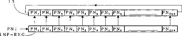
Among Fig. 4, link to each other with PN sign indicating number register 13 (Fig. 1) in corresponding stage with the same number of input PN register INP-REG of the level of PN sign indicating number register 13.Input PN register INP-REG is a shift register that coefficient data PNi is shifted towards afterbody.When the PN sign indicating number with a symbol period calculates when relevant, the PN sign indicating number sequence of next symbol period is imported into input PN register INP-REG, and before next symbol period, this input PN register INP-REG is transferred to PN sign indicating number register just.By the preparation of input PN register, the PN sign indicating number is written into fast.To be written into long code with a symbol period be effective especially to continuous for this.Fig. 3 has illustrated and shifted later state: the data identical with data in the input PN register are stored in the PN sign indicating number register.Being provided with of clock input can be independent of sampling clock, so can carry out the fast data input.
Fig. 5 has illustrated the change of the input PN register that comprises a plurality of parallel latchs.Data are by parallel these latchs that is input to, and K1 responds to CK256 to clock signal C, and any one latch receives data.Control this reception by the sampling of sampling and maintenance tap and data " 1 " or " 0 " in the maintenance register.When " 1 ", receive this data, when " 0 ", do not receive these data.Four data have been used among Fig. 5.When sampling with when keeping first tap of register SHR to preserve " 1 ", and other taps are imported into first tap of INP-REG when having preserved " 0 " in the input of first chip.When the 4th clock, the 4th tap of SHR becomes " 1 ", and other taps become " 0 ".The input of the 4th tap is imported into the 4th tap of INP-REG.According to the control of the mask register of Fig. 1, addition is carried out in four samplings, other data can be unlimited.
In Fig. 6, the input mask register INM-REG that its progression is identical with the progression of mask register 18 links to each other with mask register 18 (Fig. 1) in corresponding stage.This input mask register INM-REG is a shift register that control signal CNTi is shifted from the first order towards afterbody.When mask register 18 is controlled addition with a symbol period, next control signal of next symbol period is imported into input mask register INM-REG, just before next symbol period, this input mask register INM-REG is transferred to mask register.By the preparation of this mask register, control signal is written into fast.Being provided with of clock that is input to mask register can be independent of sampling clock CL, so a fast data input is possible.
Fig. 7 has illustrated the variation of the input mask register (Fig. 6) that comprises a plurality of parallel latchs.The control signal incoming line is connected with the level of input mask register is parallel, and each latch tap is to sampling and keep the control signal of register SHR to respond, and receives data.When mask register 18 is controlled addition with a symbol period, next control signal of next symbol period is imported into input mask register INM-REG, just before next symbol period, this input mask register INM-REG is transferred to mask register.By the preparation of this mask register, can be written into control signal fast at any time.Fig. 6 has illustrated just and shifted later state in control signal: the data identical with data in the input mask register are stored in the mask register.
Fig. 8 has illustrated the 3rd execution mode of circuit matched with wave filter, and is wherein different with the circuit among Fig. 1, and adder 15 is made jointly by a plurality of PN sign indicating number registers 13 and 16 and is used for handling.Mlultiplying circuit 14
1To 14
256Output and mlultiplying circuit 17
1To 17
256Output be imported into a multiplexer MUX7, this multiplexer MUX7 is optionally with mlultiplying circuit 14
1To 14
256Output or mlultiplying circuit 17
1To 17
256Output output to an adder 15.So an adder can be used for a plurality of result of product jointly, has reduced circuit size thus.The number of the mlultiplying circuit of selecting is many more, and with respect to total function, circuit size is more little.But, because must obtain the output of matched filter, so the number at the mlultiplying circuit of the total result of product of moment point output that can select is limited in identical moment.
An output of adder 15 is imported into the output of a selector SEL7, the output of this selector SEL7 with corresponding to mlultiplying circuit 14
1To 14
256With mlultiplying circuit 17
1To 17
256The simulation register REG71 of group link to each other with REG72.This selector 17 is with mlultiplying circuit 14
1To 14
256Output be input to register REG71, and with mlultiplying circuit 17
1To 17
256Output be input to register REG72.When matched filter output MF71 output and MF72 output, this result of product is held, and can obtain it with a rich relatively sequential.
In the above-described embodiment, PN sign indicating number sequence has different code lengths, but can be applied to the different PN sign indicating number sequences of identical code length according to matched filter banks of the present invention.
Except the de-spread of DS-CDMA communication system, this above-mentioned matched filter banks can also be carried out any calculating of other a plurality of correlated results.
Above-mentioned matched filter banks is a type real, and still, it can be applied to complex data type easily.
Be described in an execution mode of an inverting amplifier circuit that uses in the mlultiplying circuit of above-mentioned matched filter banks below with reference to Fig. 9.
In Fig. 9, the gain of this inverting amplifier circuit is variable, and it comprises input capacitance CI1 and the CI2 that receives input voltage VI1 and VI2 respectively.The output of input capacitance CI1 and CI2 is connected to the input of an amplifier AMP jointly.This amplifier AMP is an inverting amplifier that comprises the operational amplifier that its anti-phase input and input capacitance CI1 link to each other with CI2, and it also comprises the series circuit that contains odd number CMOS inverter or the circuit of other inverting amplifiers.A plurality of feedback capacity Cf1 are connected to Cf6 between the input and output of amplifier AMP, and the input and output of this amplifier AMP link to each other with a refresh switch MUXRO jointly.This feedback capacity Cf1 links to each other respectively to MUX6 with feedback multiplexer MUX1 to the input of Cf6, feedback capacity Cf1 is connected to input or a reference voltage Vref of amplifier AMP to Cf6.An amplifier refresh switch SWR is connected between the input and output of amplifier AMP, with the input and output of short circuit amplifier AMP.A refresh switch MUXR1 is connected to the input of input capacitance CI1 and CI2, to select input voltage VI1 and VI2 or reference voltage Vref.When refreshing, select Vref.Control and Feedback capacitor C f1 is responded to S6 to the control signal S1 of the validity of Cf6, switch multiplexer MUX1 to MUX6.When invalid, feedback capacity Cf1 is connected with the floating node disconnection of amplifier to the input of Cf6, and is connected to reference voltage Vref.The input (floating node) of invalid feedback capacity pair amplifier AMP is influence not.
When refreshing, refresh switch MUXRO links to each other with reference voltage Vref, and closed this refresh switch.This refresh switch MUXRI links to each other with capacitor C I1 reference voltage with CI2.Be similar to formula (1), obtained the output expression formula of this execution mode, as shown in Equation (3).
Express as following formula (4), the combination capacitor CIf of invalid feedback capacity has disappeared, and has improved output accuracy greatly.This is owing to invalid electric capacity and floating node disconnection are caused.The tradition amplifier is with different here, and this invalid feedback capacity keeps linking to each other with the output of amplifier AMP.As shown in Figure 13, the amplifier of a reality is considered to comprise the circuit of an ideal amplifier IAMP and a resistance R o who links to each other with the output of IAMP as an output impedance.When a load capacitance was CL, the relation between input VAI and the output VAOI1 as shown in Equation (4).
In formula (4), " s " is the operator of Laplace transform.For Fig. 9, when input and output are VAI ' and VAO2 respectively, can obtain a similar formula.
Can obtain a formula (6) from formula (4) and (5).
So, to compare with traditional circuit, the circuit among Fig. 9 has less error.Because refresh switch required in traditional circuit (Figure 12) is unnecessary now, so circuit size diminishes.
When the circuit gain that comes with a finite gain-bandwidth (GB) product in the presentation graphs 9, the settling time of this circuit as shown in Equation (7).
With formula (7) substitution formula (2) and (3), can obtain formula (8) and (9).
Indicial response settling time τ with a rise time τ
r, output voltage postpones and a rate of rise SR represents, as shown in Equation (10).
Here, τ
rBe one because SR time of delay of causing.When a phase compensation capacity is Cp and maximum when providing electric current to be Io, SR is provided by formula (11).
First of the right is a constant in the formula (10).One first rank transforming function transformation function H (s) as shown in Equation (12).
Rise time τ
rEqual the p1 in the formula (12) approx, as shown in Equation (13).
τ
r≌p1(13)
Compare formula (8), (9) and (10), being appreciated that can be by comparing formula (8), and the operator in (9) " s " is estimated out rise time τ
r
The parameter that is provided with is as shown in table 1, and has calculated settling time.
Table 1 parameter
| Amplifier number | ????GB | ???Io | ??CIf | ??CVf | ??Cp | ?CI1+CI2 | ?CL |
| ?S35AMP41 | ?40.35MHZ | 120μA | ?1.8pF | ?0.6Pf | ?0.2pF | ??2.4pF | ?0.5pF |
When having supposed delay time T
D1, τ
D2With rise time τ
R1, τ
R2The time, can obtain formula (14) to (18).
τ
1=τ
d1+τ
r1=5.83+198.26=204.09[nsec](18)
τ
2=τ
d2+τ
r2=20.83+123.92=144.75[nsec](19)
Along with the combination capacitor value increase of invalid electric capacity, with respect to traditional τ settling time
1, settling time τ
2Shortened.This is represented by formula (20).
Clf↑Δτ=τ
1-τ
2↑(20)
Figure 11 is the figure of an indicial response of explanation execution mode and traditional circuit.The output voltage of solid line (Vo2) and a dotted line (Vo1) expression execution mode, the output voltage of a short dash line (Vo4) and a dotted line (Vo3) expression traditional circuit.Output voltage V o1 and Vo3 are corresponding to the bank capability of the input capacitance of four specific capacitances with corresponding to the effective feedback capacity of the combination of four specific capacitances.Output voltage V o2 and Vo4 are corresponding to the bank capability of the input capacitance of eight specific capacitances with corresponding to the effective feedback capacity of the combination of eight specific capacitances.Article one, chain-dotted line (V1) is an input voltage, and REF is a refresh cycle.Input voltage is a maximum voltage, and the refresh cycle belongs to the one-period of maximum voltage.Be shorter than the settling time of Vo3 and Vo4 the settling time of Vo1 and Vo2 respectively.
Figure 10 is a scalar circuit according to the circuit among Fig. 9 (scaler circuit).This scalar circuit has an input capacitance that its effective bank capability is variable, and the gain that can obtain a wide range like this changes.The label of similar parts is identical among parts among Figure 10 and Fig. 9.
Among Figure 10, a plurality of input capacitance CI1 are connected to an input voltage V1 to CI6 jointly by a refresh switch MUXRI.When refreshing, this refresh switch MUXRI is connected to reference voltage Vref with input capacitance CI1 to the input of CI6, otherwise is connected to input voltage VI.The output of input capacitance is connected respectively to multiplexer MUX11 to MUX16, and these multiplexers MUX11 is connected to one of amplifier AMP input or reference voltage Vref to MUX16.
Control input capacitance CI1 is responded to S16 to the control signal S11 of the validity of CI6, switch multiplexer MUX11 to MUX16.When invalid, input capacitance CI1 disconnects to the output of CI6 and the floating node of amplifier and is connected and is connected to reference voltage Vref.The input (floating node) of this effective feedback electric capacity pair amplifier AMP is influence not.Similar with the circuit of Fig. 9, a plurality of feedback capacity Cf11 are connected to Cf16 between the input and output of amplifier AMP, and their output is connected to a refresh switch MUXRO jointly.Feedback circuit Cf1 links to each other respectively to MUX26 with feedback multiplexer MUX21 to the input of Cf6, feedback capacity Cf1 is connected to input or a reference voltage Vref of amplifier AMP to Cf6.An amplifier refresh switch SWR is connected between the input and output of amplifier AMP, with the input and output of short circuit amplifier AMP.A refresh switch MUXR1 is connected to the input of input capacitance CI1 and CI2, to select input voltage VI1 and VI2 or reference voltage Vref.When refreshing, select Vref.Control and Feedback capacitor C f1 is responded to S26 to the control signal S21 of the validity of Cf6, switch multiplexer MUX21 to MUX26.When invalid, feedback capacity Cf1 is connected with the floating node disconnection of amplifier to the input of Cf6, and is connected to reference voltage Vref.The input (floating node) of invalid feedback capacity pair amplifier AMP is influence not.When a bank capability of input effective capacitance is a bank capability of CVI and the invalid electric capacity of input when being CII, provide an output voltage VO of scalar circuit by formula (21).
Similar with the circuit of Fig. 9, above-mentioned this scalar circuit is accurately and is at a high speed.
Amplifier AMP is an inverting amplifier, comprises the operational amplifier that its anti-phase input links to each other with input capacitance, and it also comprises the series circuit that contains odd number CMOS inverter or the circuit of other inverting amplifiers.
Except above-mentioned execution mode, also have a kind of circuit, combinatorial input variable capacitance only, its feedback capacity is fixed.
The inverting amplifier of variable gain can not only be applied to above-mentioned matched filter, but also can be used for other circuit of an inverting amplifier of any use.
Claims (18)
1. matched filter banks comprises:
Sample and holding unit for one, be used for sampling and keep " m " individual input signal (m: be not less than 2 integer) continuously;
A plurality of numbers are the PN sign indicating number register (n: be not less than 2 integer) of " n ", each described PN sign indicating number register comprise number be the level of " m " to preserve coefficient data, each described PN sign indicating number register is a circulating register;
With the corresponding n group of described PN sign indicating number register mlultiplying circuit, each described group comprises and corresponding m mlultiplying circuit of described level of each described PN sign indicating number register that each described mlultiplying circuit is with an output of a described sampling and holding circuit and an output multiplication of a described PN sign indicating number register; With
One or more adder is selectively with the output addition of the corresponding described mlultiplying circuit of length of number and described coefficient data.
2. a matched filter banks as claimed in claim 1 further comprises:
A mask register that comprises " m " level, its preserves the control signal be used to select with the described output of the corresponding described mlultiplying circuit of described length of described coefficient data; With
With described number be that the corresponding a plurality of numbers of described mlultiplying circuit of m are the multiplexers of " m ", each described multiplexer is exported described output or " 0 " of described corresponding mlultiplying circuit selectively,
Described length with described coefficient data is corresponding thus, from the described output quilt addition selectively of described mlultiplying circuit.
3. a matched filter banks as claimed in claim 1, described sampling and holding unit comprise a plurality of samplings and the holding unit of described number for " m ".
4. a matched filter banks as claimed in claim 1, wherein said sampling and holding unit are sample shift register that progression is described " m ".
5. a matched filter banks as claimed in claim 1 further comprises:
A mask register that comprises " m " level, its preserves the control signal be used to select with the described output of the corresponding described mlultiplying circuit of described length of described coefficient data; With
A multiplexer according to the described control signal of described mask register, optionally outputs to described adder with one or more that export described in described " m " individual multiplication output.
6. a matched filter banks as claimed in claim 1, further comprise an one or more corresponding input PN sign indicating number register with described PN sign indicating number register, the described coefficient data that each described PN sign indicating number register will be preserved is saved in described PN sign indicating number register at next symbol period, and just before described next symbol period, with described coefficient data parallel transfer to described corresponding PN sign indicating number register.
7. a matched filter banks as claimed in claim 1, further comprise one and the corresponding input mask register of described mask register, described mask register is preserved the control signal that will deposit described mask register at next symbol period in, and described next symbol period before described control signal is walked abreast just and transfer to described masking register.
8. a matched filter banks as claimed in claim 6, described input PN register comprise that number is the multistage parallel latch of described " m ".
9. a matched filter banks as claimed in claim 7, described input mask register comprise that number is the multistage parallel latch of described " m ".
10. a matched filter banks as claimed in claim 1 further comprises a sampling and a retentive control circuit of controlling described sampling and holding unit.
11. a matched filter banks as claim 6 and 10, wherein said sampling and the described input PN sign indicating number register of retentive control circuit control, when the sampling of described sampling and holding unit with when keeping described input signal, synchronous constantly with this, described coefficient data is input to described input PN sign indicating number register.
12. a matched filter banks as claim 7 and 10, wherein said sampling and retentive control circuit are controlled described input mask register, when the sampling of described sampling and holding unit with when keeping described input signal, synchronous constantly with this, described control signal is input to described input mask register.
A 13. matched filter banks as claimed in claim 1, the number of wherein said adder is described group the corresponding described number of described number " n " " n " with described mlultiplying circuit, each described adder from described m the output that comes from described corresponding mlultiplying circuit with the length described output addition of described corresponding mlultiplying circuit accordingly of number and described coefficient data.
A 14. matched filter banks as claimed in claim 1, the number of wherein said adder is 1, this adder links to each other by with mlultiplying circuit described whole group of multiplexer, the mode that service time is shared, and this multiplexer optionally is connected to described adder with one in described group.
15. a matched filter banks as claimed in claim 1 further comprises a plurality of and described group of number relevant register and the selector that is connected to a described register with the described output selectivity of described adder mlultiplying circuit.
16. a matched filter banks as claimed in claim 1, each described mlultiplying circuit comprises:
One or more input capacitances with input and output, it links to each other with an input voltage in their input;
Inverting amplifier with input and output, it links to each other with the described output of described input capacitance in its input;
One or more feedback capacities with input and output, they link to each other with the described output of described inverting amplifier in their output place; With
One or more switches are used for the described output with one or more described input capacitances, and perhaps the described input of one or more described feedback capacities is connected to described input or reference voltage of described inverting amplifier.
17. a matched filter banks as claim 16, a plurality of described input capacitances wherein are provided, described switch is the corresponding input switch of a plurality of and described input capacitance, and each described input switch is connected to the described output of described corresponding input capacitance described input or reference voltage of described inverting amplifier.
18. a matched filter banks as claim 16, a plurality of described feedback capacities wherein are provided, described switch is the corresponding feedback switch of a plurality of and described feedback capacity, and each described feedback switch is connected to the described input of described respective feedback electric capacity described input or reference voltage of described inverting amplifier.
Applications Claiming Priority (4)
| Application Number | Priority Date | Filing Date | Title |
|---|---|---|---|
| JP046180/98 | 1998-02-12 | ||
| JP4618098A JPH11205193A (en) | 1997-11-14 | 1998-02-12 | Matched filter bank |
| JP10311531A JP2000138548A (en) | 1998-11-02 | 1998-11-02 | Gain variable inversion amplifier circuit |
| JP311531/98 | 1998-11-02 |
Publications (1)
| Publication Number | Publication Date |
|---|---|
| CN1231545A true CN1231545A (en) | 1999-10-13 |
Family
ID=26386296
Family Applications (1)
| Application Number | Title | Priority Date | Filing Date |
|---|---|---|---|
| CN99102307A Pending CN1231545A (en) | 1998-02-12 | 1999-02-12 | Matched filter bank |
Country Status (4)
| Country | Link |
|---|---|
| US (1) | US6512785B1 (en) |
| EP (1) | EP0936748A3 (en) |
| KR (1) | KR100324259B1 (en) |
| CN (1) | CN1231545A (en) |
Cited By (2)
| Publication number | Priority date | Publication date | Assignee | Title |
|---|---|---|---|---|
| WO2003007519A1 (en) * | 2001-07-11 | 2003-01-23 | Linkair Communications, Inc. | A match filter for code division multiple access communication system |
| CN109388882A (en) * | 2018-10-08 | 2019-02-26 | 北京理工大学 | A kind of staggeredly matched filtering method suitable for ASIC Design |
Families Citing this family (33)
| Publication number | Priority date | Publication date | Assignee | Title |
|---|---|---|---|---|
| US7515896B1 (en) | 1998-10-21 | 2009-04-07 | Parkervision, Inc. | Method and system for down-converting an electromagnetic signal, and transforms for same, and aperture relationships |
| US6061551A (en) * | 1998-10-21 | 2000-05-09 | Parkervision, Inc. | Method and system for down-converting electromagnetic signals |
| US7039372B1 (en) * | 1998-10-21 | 2006-05-02 | Parkervision, Inc. | Method and system for frequency up-conversion with modulation embodiments |
| US6370371B1 (en) * | 1998-10-21 | 2002-04-09 | Parkervision, Inc. | Applications of universal frequency translation |
| US7236754B2 (en) * | 1999-08-23 | 2007-06-26 | Parkervision, Inc. | Method and system for frequency up-conversion |
| US6813485B2 (en) * | 1998-10-21 | 2004-11-02 | Parkervision, Inc. | Method and system for down-converting and up-converting an electromagnetic signal, and transforms for same |
| US6873836B1 (en) * | 1999-03-03 | 2005-03-29 | Parkervision, Inc. | Universal platform module and methods and apparatuses relating thereto enabled by universal frequency translation technology |
| US6879817B1 (en) | 1999-04-16 | 2005-04-12 | Parkervision, Inc. | DC offset, re-radiation, and I/Q solutions using universal frequency translation technology |
| US6853690B1 (en) | 1999-04-16 | 2005-02-08 | Parkervision, Inc. | Method, system and apparatus for balanced frequency up-conversion of a baseband signal and 4-phase receiver and transceiver embodiments |
| US7110435B1 (en) * | 1999-03-15 | 2006-09-19 | Parkervision, Inc. | Spread spectrum applications of universal frequency translation |
| JP3771390B2 (en) * | 1999-03-16 | 2006-04-26 | 富士通株式会社 | Matched filter |
| US7065162B1 (en) | 1999-04-16 | 2006-06-20 | Parkervision, Inc. | Method and system for down-converting an electromagnetic signal, and transforms for same |
| US7110444B1 (en) * | 1999-08-04 | 2006-09-19 | Parkervision, Inc. | Wireless local area network (WLAN) using universal frequency translation technology including multi-phase embodiments and circuit implementations |
| US7693230B2 (en) * | 1999-04-16 | 2010-04-06 | Parkervision, Inc. | Apparatus and method of differential IQ frequency up-conversion |
| US7412018B1 (en) * | 1999-05-26 | 2008-08-12 | Alcatel Usa Sourcing, L.P. | Rapid acquisition synchronization sequences for direct sequence spread spectrum systems using code time offsets |
| US8295406B1 (en) | 1999-08-04 | 2012-10-23 | Parkervision, Inc. | Universal platform module for a plurality of communication protocols |
| AU1610601A (en) * | 1999-11-15 | 2001-05-30 | Massachusetts Institute Of Technology | A nonlinear dynamic system for spread spectrum code generation and acquisition |
| US6724805B1 (en) | 1999-11-15 | 2004-04-20 | Massachusetts Institute Of Technology | Nonlinear dynamic system for spread spectrum code generation and acquisition |
| US7082171B1 (en) * | 1999-11-24 | 2006-07-25 | Parkervision, Inc. | Phase shifting applications of universal frequency translation |
| JP3453100B2 (en) * | 2000-03-31 | 2003-10-06 | 松下電器産業株式会社 | Matched filter and operation method in matched filter |
| US7010286B2 (en) | 2000-04-14 | 2006-03-07 | Parkervision, Inc. | Apparatus, system, and method for down-converting and up-converting electromagnetic signals |
| US7010559B2 (en) * | 2000-11-14 | 2006-03-07 | Parkervision, Inc. | Method and apparatus for a parallel correlator and applications thereof |
| US7454453B2 (en) * | 2000-11-14 | 2008-11-18 | Parkervision, Inc. | Methods, systems, and computer program products for parallel correlation and applications thereof |
| JP4642264B2 (en) * | 2001-04-03 | 2011-03-02 | 株式会社日立国際電気 | Correlation circuit for spread spectrum communication |
| US7072427B2 (en) * | 2001-11-09 | 2006-07-04 | Parkervision, Inc. | Method and apparatus for reducing DC offsets in a communication system |
| US7103091B2 (en) * | 2002-05-07 | 2006-09-05 | Stmicroelectronics, Inc. | Common data path rake receiver for a CDMA demodulator circuit |
| US7460584B2 (en) * | 2002-07-18 | 2008-12-02 | Parkervision, Inc. | Networking methods and systems |
| US7379883B2 (en) | 2002-07-18 | 2008-05-27 | Parkervision, Inc. | Networking methods and systems |
| US7209867B2 (en) | 2002-10-15 | 2007-04-24 | Massachusetts Institute Of Technology | Analog continuous time statistical processing |
| CN101095232B (en) * | 2003-07-16 | 2010-12-08 | Nxp股份有限公司 | Input stage resistant against negative voltage swings |
| US7084713B2 (en) * | 2004-03-29 | 2006-08-01 | Qualcomm Inc. | Programmable capacitor bank for a voltage controlled oscillator |
| US7512172B2 (en) * | 2004-09-30 | 2009-03-31 | Yan Zhang | Path search method for CDMA communication systems |
| US10396846B1 (en) * | 2018-10-12 | 2019-08-27 | Cisco Technology, Inc. | Adaptive decoding of spread spectrum signals using multiple correlator peaks |
Family Cites Families (9)
| Publication number | Priority date | Publication date | Assignee | Title |
|---|---|---|---|---|
| DE3735374A1 (en) * | 1987-10-19 | 1989-05-03 | Siemens Ag | Digital correlator circuit |
| US5604458A (en) * | 1993-02-05 | 1997-02-18 | Yozan Inc. | Scaler circuit |
| EP0741366B1 (en) * | 1995-04-26 | 2001-02-14 | Yozan Inc. | Multiplication circuit |
| DE69634974D1 (en) * | 1995-12-26 | 2005-09-01 | Sharp Kk | Spreizspektrumnachrichtenübertragungssystem |
| JP3476987B2 (en) * | 1996-01-12 | 2003-12-10 | 株式会社日立国際電気 | Multi-user demodulation method and apparatus |
| US5696762A (en) * | 1996-03-25 | 1997-12-09 | Stanford Telecommunications, Inc. | Rapid-acquisition access channel scheme for CDMA systems |
| JPH10229378A (en) * | 1996-04-02 | 1998-08-25 | Sharp Corp | Matched filter |
| JP3323760B2 (en) * | 1996-11-07 | 2002-09-09 | 株式会社日立製作所 | Spread spectrum communication system |
| EP0884856A3 (en) * | 1997-06-09 | 2002-04-10 | Yozan Inc. | Spread spectrum communication system |
-
1999
- 1999-02-10 KR KR1019990004595A patent/KR100324259B1/en not_active IP Right Cessation
- 1999-02-10 EP EP99102550A patent/EP0936748A3/en not_active Withdrawn
- 1999-02-11 US US09/247,828 patent/US6512785B1/en not_active Expired - Lifetime
- 1999-02-12 CN CN99102307A patent/CN1231545A/en active Pending
Cited By (3)
| Publication number | Priority date | Publication date | Assignee | Title |
|---|---|---|---|---|
| WO2003007519A1 (en) * | 2001-07-11 | 2003-01-23 | Linkair Communications, Inc. | A match filter for code division multiple access communication system |
| CN109388882A (en) * | 2018-10-08 | 2019-02-26 | 北京理工大学 | A kind of staggeredly matched filtering method suitable for ASIC Design |
| CN109388882B (en) * | 2018-10-08 | 2022-11-04 | 北京理工大学 | Staggered matched filtering method suitable for special integrated circuit design |
Also Published As
| Publication number | Publication date |
|---|---|
| EP0936748A3 (en) | 2003-07-23 |
| KR19990072548A (en) | 1999-09-27 |
| US6512785B1 (en) | 2003-01-28 |
| EP0936748A2 (en) | 1999-08-18 |
| KR100324259B1 (en) | 2002-02-21 |
Similar Documents
| Publication | Publication Date | Title |
|---|---|---|
| CN1231545A (en) | Matched filter bank | |
| CN1168241C (en) | Method and device for making code synchronous trapping in CDMA communication system | |
| CN1190016C (en) | Device for obtaining pseudo-noise code and direct DSDMA receiver | |
| CN1232317A (en) | Matched filter and signal reception apparatus | |
| CN1090882C (en) | Expanded spectrum receiver for communication system | |
| CN1249090A (en) | Method and arrangement for despreading coded sequence in communication system | |
| CN101478361B (en) | Constructing apparatus for multi-dimension quasi-orthogonal pseudo-random matrix | |
| CN101414890A (en) | Method for composing multidimensional quadrature pseudo-random matrix | |
| CN103152070A (en) | Variable beacon sequence-based spread spectrum communication method | |
| CN1146666A (en) | Circuit matched with wave filter | |
| CN1688119A (en) | Method for testing DS. CDMA system multi-user developed based on weighting | |
| CN1102305C (en) | Matched filter circuit used for frequency-expansion communication | |
| CN1890890A (en) | Station comprising a rake receiver | |
| CN2704159Y (en) | Subscriber unit for processing and receiving CDMA communication data | |
| CN102158199B (en) | Method and device for selecting pre-stored filter coefficient set in time-varying system | |
| CN1192509C (en) | CDMA modulation method and device thereof | |
| CN1255780A (en) | Matched filter circuit | |
| CN1201514C (en) | Implement method of ternary spread spectrum sequence coding in CDMA system | |
| CN1191431A (en) | Symbolic division multiple communication apparatus | |
| CN1196292C (en) | Device for acquiring initial synchronous codes in CDMA communication system and method thereof | |
| CN1398460A (en) | Methods and appts. for signal searching using correlation | |
| CN1611015A (en) | Receiving apparatus | |
| CN1160307A (en) | Matched filter circuit | |
| JP2005101695A (en) | Correlation detecting apparatus | |
| CN103475382B (en) | A kind of Zero intermediate frequency Gaussian white noise adding method and device |
Legal Events
| Date | Code | Title | Description |
|---|---|---|---|
| C06 | Publication | ||
| PB01 | Publication | ||
| C10 | Entry into substantive examination | ||
| SE01 | Entry into force of request for substantive examination | ||
| C10 | Entry into substantive examination | ||
| SE01 | Entry into force of request for substantive examination | ||
| C02 | Deemed withdrawal of patent application after publication (patent law 2001) | ||
| WD01 | Invention patent application deemed withdrawn after publication |