CN1229871C - Micro-LED arrays with enhanced light extraction - Google Patents
Micro-LED arrays with enhanced light extraction Download PDFInfo
- Publication number
- CN1229871C CN1229871C CNB008166013A CN00816601A CN1229871C CN 1229871 C CN1229871 C CN 1229871C CN B008166013 A CNB008166013 A CN B008166013A CN 00816601 A CN00816601 A CN 00816601A CN 1229871 C CN1229871 C CN 1229871C
- Authority
- CN
- China
- Prior art keywords
- light
- emitting diode
- layer
- little light
- dispersion layer
- Prior art date
- Legal status (The legal status is an assumption and is not a legal conclusion. Google has not performed a legal analysis and makes no representation as to the accuracy of the status listed.)
- Expired - Lifetime
Links
- 238000003491 array Methods 0.000 title abstract description 3
- 238000000605 extraction Methods 0.000 title abstract 4
- 239000006185 dispersion Substances 0.000 claims description 72
- 239000000758 substrate Substances 0.000 claims description 37
- 239000004065 semiconductor Substances 0.000 claims description 24
- 230000004888 barrier function Effects 0.000 claims description 18
- 229910052751 metal Inorganic materials 0.000 claims description 14
- 239000002184 metal Substances 0.000 claims description 14
- 238000009413 insulation Methods 0.000 claims description 7
- 238000000034 method Methods 0.000 abstract description 23
- 230000001965 increasing effect Effects 0.000 abstract description 9
- 229910052737 gold Inorganic materials 0.000 description 14
- 238000010276 construction Methods 0.000 description 13
- 239000000463 material Substances 0.000 description 13
- 239000011159 matrix material Substances 0.000 description 12
- 238000005516 engineering process Methods 0.000 description 8
- 238000005530 etching Methods 0.000 description 8
- 229910052763 palladium Inorganic materials 0.000 description 7
- 238000001020 plasma etching Methods 0.000 description 7
- 229910052697 platinum Inorganic materials 0.000 description 7
- 229910010271 silicon carbide Inorganic materials 0.000 description 6
- 239000004020 conductor Substances 0.000 description 5
- 230000003993 interaction Effects 0.000 description 5
- 229920000642 polymer Polymers 0.000 description 5
- VYPSYNLAJGMNEJ-UHFFFAOYSA-N Silicium dioxide Chemical compound O=[Si]=O VYPSYNLAJGMNEJ-UHFFFAOYSA-N 0.000 description 4
- 229910052759 nickel Inorganic materials 0.000 description 4
- 229910052594 sapphire Inorganic materials 0.000 description 4
- 239000010980 sapphire Substances 0.000 description 4
- 229910000980 Aluminium gallium arsenide Inorganic materials 0.000 description 3
- 229910045601 alloy Inorganic materials 0.000 description 3
- 239000000956 alloy Substances 0.000 description 3
- 230000008901 benefit Effects 0.000 description 3
- 238000000151 deposition Methods 0.000 description 3
- 238000004519 manufacturing process Methods 0.000 description 3
- 150000004767 nitrides Chemical class 0.000 description 3
- 230000000737 periodic effect Effects 0.000 description 3
- 238000007639 printing Methods 0.000 description 3
- 230000001902 propagating effect Effects 0.000 description 3
- 230000000717 retained effect Effects 0.000 description 3
- 229910052709 silver Inorganic materials 0.000 description 3
- 239000000126 substance Substances 0.000 description 3
- 229910001218 Gallium arsenide Inorganic materials 0.000 description 2
- 239000004793 Polystyrene Substances 0.000 description 2
- 238000002679 ablation Methods 0.000 description 2
- 238000010521 absorption reaction Methods 0.000 description 2
- 230000005540 biological transmission Effects 0.000 description 2
- 230000008859 change Effects 0.000 description 2
- 238000005229 chemical vapour deposition Methods 0.000 description 2
- 238000001312 dry etching Methods 0.000 description 2
- 230000000694 effects Effects 0.000 description 2
- 230000008020 evaporation Effects 0.000 description 2
- 238000001704 evaporation Methods 0.000 description 2
- 239000010408 film Substances 0.000 description 2
- 238000010438 heat treatment Methods 0.000 description 2
- 230000006872 improvement Effects 0.000 description 2
- 238000002955 isolation Methods 0.000 description 2
- 229920002223 polystyrene Polymers 0.000 description 2
- 230000008569 process Effects 0.000 description 2
- 238000004064 recycling Methods 0.000 description 2
- 230000011218 segmentation Effects 0.000 description 2
- 239000000377 silicon dioxide Substances 0.000 description 2
- 239000010409 thin film Substances 0.000 description 2
- 238000005452 bending Methods 0.000 description 1
- 230000008033 biological extinction Effects 0.000 description 1
- 229910052681 coesite Inorganic materials 0.000 description 1
- 239000002131 composite material Substances 0.000 description 1
- 150000001875 compounds Chemical class 0.000 description 1
- 229910052906 cristobalite Inorganic materials 0.000 description 1
- 238000005520 cutting process Methods 0.000 description 1
- 230000008021 deposition Effects 0.000 description 1
- 238000007599 discharging Methods 0.000 description 1
- 230000005611 electricity Effects 0.000 description 1
- 238000010894 electron beam technology Methods 0.000 description 1
- 238000005538 encapsulation Methods 0.000 description 1
- 230000002708 enhancing effect Effects 0.000 description 1
- 239000003822 epoxy resin Substances 0.000 description 1
- 230000001747 exhibiting effect Effects 0.000 description 1
- 239000012634 fragment Substances 0.000 description 1
- 239000011521 glass Substances 0.000 description 1
- 239000008187 granular material Substances 0.000 description 1
- 230000017525 heat dissipation Effects 0.000 description 1
- 238000005286 illumination Methods 0.000 description 1
- 230000008676 import Effects 0.000 description 1
- 239000012212 insulator Substances 0.000 description 1
- 230000007246 mechanism Effects 0.000 description 1
- 238000006263 metalation reaction Methods 0.000 description 1
- 238000001465 metallisation Methods 0.000 description 1
- 150000002739 metals Chemical class 0.000 description 1
- 239000004005 microsphere Substances 0.000 description 1
- 239000000203 mixture Substances 0.000 description 1
- 230000004048 modification Effects 0.000 description 1
- 238000012986 modification Methods 0.000 description 1
- 230000003287 optical effect Effects 0.000 description 1
- 230000002093 peripheral effect Effects 0.000 description 1
- 229920000647 polyepoxide Polymers 0.000 description 1
- 230000000644 propagated effect Effects 0.000 description 1
- 230000005855 radiation Effects 0.000 description 1
- 230000009467 reduction Effects 0.000 description 1
- -1 semimetal Substances 0.000 description 1
- 235000012239 silicon dioxide Nutrition 0.000 description 1
- 239000007787 solid Substances 0.000 description 1
- 238000001228 spectrum Methods 0.000 description 1
- 229910052682 stishovite Inorganic materials 0.000 description 1
- 238000005728 strengthening Methods 0.000 description 1
- 229910052905 tridymite Inorganic materials 0.000 description 1
Images


Classifications
-
- H—ELECTRICITY
- H01—ELECTRIC ELEMENTS
- H01L—SEMICONDUCTOR DEVICES NOT COVERED BY CLASS H10
- H01L33/00—Semiconductor devices with at least one potential-jump barrier or surface barrier specially adapted for light emission; Processes or apparatus specially adapted for the manufacture or treatment thereof or of parts thereof; Details thereof
- H01L33/02—Semiconductor devices with at least one potential-jump barrier or surface barrier specially adapted for light emission; Processes or apparatus specially adapted for the manufacture or treatment thereof or of parts thereof; Details thereof characterised by the semiconductor bodies
- H01L33/08—Semiconductor devices with at least one potential-jump barrier or surface barrier specially adapted for light emission; Processes or apparatus specially adapted for the manufacture or treatment thereof or of parts thereof; Details thereof characterised by the semiconductor bodies with a plurality of light emitting regions, e.g. laterally discontinuous light emitting layer or photoluminescent region integrated within the semiconductor body
-
- H—ELECTRICITY
- H01—ELECTRIC ELEMENTS
- H01L—SEMICONDUCTOR DEVICES NOT COVERED BY CLASS H10
- H01L33/00—Semiconductor devices with at least one potential-jump barrier or surface barrier specially adapted for light emission; Processes or apparatus specially adapted for the manufacture or treatment thereof or of parts thereof; Details thereof
- H01L33/36—Semiconductor devices with at least one potential-jump barrier or surface barrier specially adapted for light emission; Processes or apparatus specially adapted for the manufacture or treatment thereof or of parts thereof; Details thereof characterised by the electrodes
- H01L33/38—Semiconductor devices with at least one potential-jump barrier or surface barrier specially adapted for light emission; Processes or apparatus specially adapted for the manufacture or treatment thereof or of parts thereof; Details thereof characterised by the electrodes with a particular shape
-
- H—ELECTRICITY
- H01—ELECTRIC ELEMENTS
- H01L—SEMICONDUCTOR DEVICES NOT COVERED BY CLASS H10
- H01L33/00—Semiconductor devices with at least one potential-jump barrier or surface barrier specially adapted for light emission; Processes or apparatus specially adapted for the manufacture or treatment thereof or of parts thereof; Details thereof
- H01L33/02—Semiconductor devices with at least one potential-jump barrier or surface barrier specially adapted for light emission; Processes or apparatus specially adapted for the manufacture or treatment thereof or of parts thereof; Details thereof characterised by the semiconductor bodies
- H01L33/20—Semiconductor devices with at least one potential-jump barrier or surface barrier specially adapted for light emission; Processes or apparatus specially adapted for the manufacture or treatment thereof or of parts thereof; Details thereof characterised by the semiconductor bodies with a particular shape, e.g. curved or truncated substrate
- H01L33/22—Roughened surfaces, e.g. at the interface between epitaxial layers
-
- H—ELECTRICITY
- H01—ELECTRIC ELEMENTS
- H01L—SEMICONDUCTOR DEVICES NOT COVERED BY CLASS H10
- H01L33/00—Semiconductor devices with at least one potential-jump barrier or surface barrier specially adapted for light emission; Processes or apparatus specially adapted for the manufacture or treatment thereof or of parts thereof; Details thereof
- H01L33/36—Semiconductor devices with at least one potential-jump barrier or surface barrier specially adapted for light emission; Processes or apparatus specially adapted for the manufacture or treatment thereof or of parts thereof; Details thereof characterised by the electrodes
- H01L33/40—Materials therefor
- H01L33/42—Transparent materials
Abstract
This invention describes new LED structures that provide increased light extraction efficiency. The new LED structures include arrays of electrically interconnected micro-LEDs that have and active layer sandwiched between two oppositely doped layer. The micro-LEDs are formed on a first spreader layer with the bottom layer of the micro-LEDs in contact with the first spreader. A second spreader layer is formed over the micro-LEDs and in contact with their top layer. The first spreader layer is electrically isolated from the second spreader layer. Each of the spreader layers has a contact and when a bias is applied across the contacts, current spreads to the micro-LEDs and they emit light. The efficiency of the new LED is increased by the increased emission surface of the micro-LEDs. Light from each of the micro-LEDs active layer will reach a surface after travelling only a short distance, reducing total internal reflection of the light. Light extraction elements (LEEs) between the micro-LEDs can be included to further enhance light extraction. The new LEDs are fabricated with standard processing techniques making them highly manufacturable at costs similar to standard LEDs.
Description
The application requires the right of people such as Thibeault in No. the 60/168th, 817, the U.S. Provisional Application case of application on December 3rd, 1999.
Technical field
The present invention relates to a kind of light-emitting diode, more particularly, relate to the new construction that a kind of light of strengthening described light-emitting diode is emitted.
Background technology
Light-emitting diode (LEDs) is a kind of important solid device that converts electrical energy into light, and this device comprises the active layer of semiconductor material usually, and it is clipped in two on the contrary between the doped layer.When a bias voltage was applied to this doped layer, hole and electronics were injected into this active layer and compound therein and produce light.By the light theaomni-directional transmission that this active region produced, and from all exposures this device of overflowing.The light that the shell of this light-emitting diode is commonly used to overflow imports a desired output emission section.
When semi-conducting material improved, the efficient of those semiconductor devices also had improvement.New light-emitting diodes is effective similarly to be the material of GaN, and this material provides the effective illumination in the yellow spectrum scope is arrived in ultraviolet ray.Many new light-emitting diodes are more efficient and can be more reliable than traditional lamp to the light time at converting electrical energy.Because light-emitting diode has improved, it is expected to replace traditional lamp, for example traffic signals, outdoor and indoor display, auto bulb and taillight, conventional room lighting or the like in many application.
Yet the limited efficiency of traditional light-emitting diode can not be launched the light that all are produced by its active layer in it.When a light-emitting diode was energized, the light of being launched by its active layer (omnidirectional ground) arrived the surface of emissions with many different angles.Typical semi-conducting material is compared with the epoxy resin (n is about 1.5) of surrounding air (refractive index n equals 1.0) or encapsulation, has a higher refractive index (n is about 2.2 to 3.8).According to Snell's law, light propagate into from a place with high index one have low refractive index local time, as this light (with respect to this surface normal direction) within a certain critical angle, will pass and arrive the lower place of this index.This light then can not pass when arriving this curved surface greater than critical angle, and can experience total internal reflection (TIR).Under the situation of a light-emitting diode, this TIR light can constantly reflect in this light-emitting diode, and till it is absorbed, or it can be overflowed from the surface that is different from this surface of emission.Because this phenomenon is not launched by the light that traditional light-emitting diode produced in a large number, and efficient is reduced.
A kind of method of percentage of the TIR of reduction light is the light scattering center that will produce the random structure pattern on the surface of light-emitting diode.[proposing " 30% External Quantum Efficiency fromSurface Textured, Thin Film Light Emitting Diodes ", Applied Physics Letters63, page or leaf 2174-2176 (1993) by people such as Shnitzer].This random structure is during reactive ion etching, by using the sub-micron diameter granules of polystyrene to take shape on this surface as a mask on this LED surface.This structurized surface has the characteristics aspect light wavelength, so that the refraction of light and reflection way are because this effect of stochastic disturbance and can't being predicted by Snell's law.The method shows can improve emission effciency 9% to 30%.
A shortcoming of this surface texture is that it has the light-emitting diode of electrode layers structure of poor conductivity at those, p-type GaN for example, and this surface texture can hinder effective electric current to disperse.At less device or have in the device of satisfactory electrical conductivity, can flow into from the electric current of this p and n type layer contact point and to spread all over each layer.And for bigger device or the device made with the poor conductivity material, electric current can't spread all over each layer by this contact point.Therefore, partly this active layer can not receive this electric current and can not launch light.Inject in order to produce uniform electric current at whole diode area, an electric conducting material dispersion layer can deposit in its surface.Yet, this dispersion layer must be usually printing opacity so that light can see through this layer.When a random surface structure is introduced on this LED surface, then can not deposit the electric current dispersion layer of an enough thin and printing opacity easily.
The method that another light that increases by a light-emitting diode is emitted is to comprise a periodic pattern at this emitting surface or internal interface, and it can be caught the angle from the benefit of its inside with light and lead again with the definition mode of being determined by this surface configuration and pattern.Please refer to the U.S. Patent number 5,779,924 of authorizing people such as Krames.This technology is a particular example on a random structure surface, and wherein this disturbing effect no longer is at random, and should can will couple light to special pattern or direction in the surface.A shortcoming of the method is that this structure is difficult to make, because this surface configuration and pattern must be uniformly, and very little, little to the single wavelength that is equivalent to this light emitting diode light.This pattern also brings difficulty for the electric current dispersion layer of deposition one printing opacity, as previously mentioned.
Increasing light emits also and can have the hemisphere of an emitting layer at the center by the emitting surface of this light-emitting diode being made one.When this structure increased the amount of radiating light, its making also was difficult to.In the U.S. Patent number 3,954,534 to Scifres and Burnham, disclosed the array that forms a kind of light-emitting diode, a hemisphere has been arranged respectively on each light-emitting diode.This hemisphere system is formed in the substrate, and diode array increases thereon.Then, the etching from this substrate of this diode and lens arrangement is removed.The shortcoming of the method is that it is limited to this structure is formed on this substrate interface, and removes the increase that this structure can cause manufacturing cost from this substrate.Simultaneously, each hemisphere all have an emitting layer directly the position thereon, it needs very accurate manufacturing.
U.S. Patent number 5,793,062 discloses a kind of structure, its light that is used to strengthen from a light-emitting diode is emitted, light is led again leave the absorption region by comprising not the non-absorbed layer of extinction, contact point for example, and make the surface direction changed course of light towards this light-emitting diode.A shortcoming of this structure is that this non-absorbed layer need form the narrow angle layer of cutting the end, and many material systems are very difficult to make.
Adding another method that high light emits is within the thin film metal layer on the surface of emission of this light-emitting diode photon to be coupled to the surface plasmon pattern, and those photons are launched gets back to radiation mode.[people's such as Knock, " Strongly Directional Emission from AlGaAs/GaAs Light EmittingDiodes ", Applied Physics Letter 57, page or leaf 2327-2329, (1990)].The photon that this semiconductor emission is returned in these structures dependences is coupled to the surface plasmon in this metal level, and it further is coupled with the photon of finally being emitted.A shortcoming of this device is that it is difficult to make, because the one-dimensional ruled grating that this periodic structure is a ditch depth extremely shallow (<0.1 micron).Simultaneously, overall outer quantum efficiency very low (1.4-1.5%) is likely because the efficient that photon is changed the mechanism to the environment photon to surface plasmon and surface plasmon is low.This structure also can be brought the same difficulty relevant with an electric current dispersion layer, as mentioned above.
Improving that light emits also can be inverted truncated cone-shaped to produce one at an angle by the side that makes the light-emitting diodes section of jurisdiction.This surface at an angle provide one within critical angle emitting surface to be retained in this baseplate material TIR light [people's such as Krames, ' High Power Truncated Inverted Pyramid (AlxGal-x) 0.5In0.5P/GaP Light Emitting Diodes Exhibiting>50% ExternalQuantum Efficiency ', Applied Physics Letters 75 (1999)].By the method, for the InGaAlP material system, the external quantum efficiency of being showed has increased by 35% to 50%.The method is feasible for the device that a large amount of light are retained in this substrate.As under the situation of growth GaN on the sapphire substrate, only be retained in a large number in the GaN film, so that the side of light-emitting diode sheet can not reach desired gain at an angle.
Other has, and a kind of to add the method that high light emits be the recycling [people such as Shnitzer of photon, ' Ultrahighspontaneous emission quantum efficiency, 99.7% internally and 72%externally, from AlGaAs/GaAs/AlGaAs double heterostructures ', AppliedPhysics Letters 62, page or leaf 131-133, (1993)].The method relies on the light-emitting diode with a high efficiency active layer, and this active layer can convert electronics and hole to light immediately, and vice versa.TIR light is reflected by this LED surface, and strikes this active layer, thereby is converted back to an electron-hole pair.Because the high efficiency of this active layer, this electron-hole pair almost is converted to light immediately, and launches to random direction once more.The recycling light of a certain percentage will be overflowed come to beat less than critical angle at one of them surface of emission of light-emitting diode.And the light that reflects back into this active layer can experience same process once more.Yet the method only can be used in the light-emitting diode made from the low-down material of optical loss, and can not be used for having in its surface the light-emitting diode of an absorption current dispersion layer.
Summary of the invention
The invention provides a kind of new light-emitting diode, it has little light emitting diode matrix of interconnection, emits with the light that improvement is provided.Little light-emitting diode has a less active region, and its scope is at 1 to 2500 square micron, but this size is not a key of the present invention.The array of one little light-emitting diode is that any little light-emitting diode with electrical interconnection distributes.This array provides a big surface area, makes light each little light-emitting diode of can overflowing, this and increase the available light of light-emitting diode.Described new light-emitting diode can have many different geometries, and because it is to form with the standard semiconductor treatment technology, so be highly susceptible to making.
This new light-emitting diode comprises one first conduction dispersion layer, deposits some little light-emitting diodes on its surface.Each little light-emitting diode all has a p-type layer, and a n-type layer and is clipped in the active layer between described p-and the n-type layer.Described p-or n-type layer all can be the upper strata, and another then can be lower floor.The electric current that puts on described first dispersion layer can be distributed to the lower floor of each little light-emitting diode.One second dispersion layer is included on described little light-emitting diode, and can be distributed to described upper strata from the electric current of described second dispersion layer.When a bias voltage was applied to described first and second dispersion layer, little light-emitting diode was promptly luminous.
One embodiment of described second dispersion layer is the lattice-shaped structure of the interconnection of a conduction, and it has the conductive path on described little light-emitting diode, and those paths contact with the upper strata of described little light-emitting diode.One insulating barrier is included on the described array, and described grid is on this insulating barrier, therefore with described first dispersion layer and described grid electric insulation.
In addition, available flip-chip engages and makes little light-emitting diode interconnection.Use the method, at first form a little light emitting diode matrix that does not connect, make it join a conductive material to then so that this array interconnect.In one the 3rd embodiment, described grid is by little light-emitting diode, and described p-type, active layer, and n-section bar material this slightly under the conductive path of the grid between the light-emitting diode with this grid and the first dispersion layer electric insulation.This lattice-shaped structure can be designed to make the light of emission to interact with a sidewall after propagating one section short distance.
Described new light-emitting diode can make light emit assembly (LEEs) and be deposited on this slightly between the light-emitting diode, or is formed on this slightly on the side of light-emitting diode, emits further to add high light.Those LEEs are used for making turn light rays or the focusing in a standard light emitting diode construction, otherwise light will be trapped or absorbs by TIR.The shape of LEEs can be curved surface (protrude or recessed), or the fragment linearity, and the shape of this structure can influence that light is emitted and light finally emit direction.LEEs between described little light-emitting diode interacts with the light of overflowing from this little led sides.This interaction helps to prevent that the light that reflects back into this light-emitting diode is absorbed, and has therefore increased the using light that is come out by this light-emitting diode.
Be described in detail and in conjunction with the accompanying drawings by following, those skilled in the art will understand these and other further feature and advantage of the present invention, wherein:
Description of drawings
Figure 1 shows that one has the plane graph of the new light-emitting diode of a little light emitting diode matrix, this little light emitting diode matrix has an interconnection electric current on an electric insulation layer and disperses grid;
Figure 2 shows that this new light-emitting diode is along the profile of section line 2-2 among Fig. 1;
Figure 3 shows that the profile of another embodiment of this new light-emitting diode, its little light emitting diode matrix utilizes flip-over type to install and joins fixed bed to one time;
The conductive interconnection electric current that Figure 4 shows that one the 3rd embodiment of this new light-emitting diode disperses the plane graph of grid and the semi-conducting material below this grid path;
Figure 5 shows that this light-emitting diode is along the profile of section line 4-4 among Fig. 4;
Figure 6 shows that another interconnection electric current disperses the plane graph of grid;
Figure 7 shows that another interconnection electric current disperses the plane graph of grid;
Figure 8 shows that can be within this little light-emitting diode the profile of the basic configuration of the LEEs of combination;
Figure 9 shows that the profile that has at this new light-emitting diode of this different LEEs that forms between light-emitting diode slightly;
Figure 10 shows that and have with the profile of this new light-emitting diode of the LEEs of form structured surface at random;
Figure 11 shows that the profile of this little light emitting diode matrix among Figure 10, it has one and directly is positioned at this electric current and disperses current blocked layer below grid;
Figure 12 shows that the profile that has with this new light-emitting diode of the side all-in-one-piece LEEs of little light-emitting diode;
Figure 13 shows that the profile of this new light-emitting diode with the curved surface LEEs that combines with the side of little light-emitting diode;
Figure 14 shows that the profile that has with this new light-emitting diode of the side of little light-emitting diode and the middle curved surface LEEs that combines; And
Figure 15 shows that as among Fig. 4 but have the profile of this new light-emitting diode of the LEEs of curved surface.
Embodiment
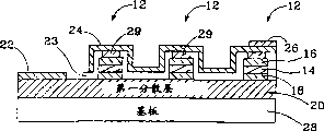
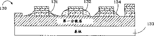
Fig. 1 and 2 is depicted as an embodiment of this new light-emitting diode 10 constructed according to the invention.This light-emitting diode comprises the array of a little light-emitting diode 12, and each little light-emitting diode 12 is all isolated, and has the active layer of semiconductor material 14 between the opposite doped layer 16 of being clipped in of itself and 18.In preferable little light-emitting diode, its upper strata 16 is the p-type, and lower floor 18 is the n-type, although layer 16 and layer 18 doping on the contrary still can be operated.
This new light-emitting diode also comprises one first dispersion layer 20, and it is distributed to electric current the lower floor 18 of each little light-emitting diode by n-contact point 22.It is because the lower floor 18 in this preferred embodiment is the n-type that this contact point 22 is called the n-contact point.One insulating barrier 23 is deposited on this little light emitting diode matrix, and it has covered the surface of first dispersion layer in each little light-emitting diode and the groove between little light-emitting diode.One second dispersion layer, it preferably disperses the form of grid 24 to be deposited on this insulating barrier with an interconnection electric current, and the conductive path of this insulating barrier and grid crosses on the light-emitting diode slightly at this.One p-contact point 26 is deposited on this grid 24, and is distributed to the upper strata 16 of each little light-emitting diode 12 by this grid from the electric current of this contact point.This contact point 26 is referred to as the p-contact point, because the upper strata in this preferred embodiment 16 is the p-type.
One hole is formed on each little light-emitting diode and passes described insulating barrier, and a little light-emitting diode contact point 29 is included in each insulating barrier hole with as the contact point between the upper strata 16 of grid 24 and little light-emitting diode.The surface of described little light-emitting diode (except the hole) and described first dispersion layer disperses the grid electric insulation by described insulating barrier 23 and described electric current.Total on a substrate 28, form and this slightly light-emitting diode form an array and put on contact point 22 and at 26 o'clock promptly luminous at a bias voltage.In another embodiment, a transparent conductive sheets is used as second dispersion layer and replaces grid 24.
This new light-emitting diode 10 has the light emission of enhancing, and being increases because of little light-emitting diode of its surface of emission by those isolation.Only after a bit of distance, promptly interact by the light that active layer produced of each little light-emitting diode with the edge of this little light-emitting diode.If this light is within this critical angle, it can be overflowed from little light-emitting diode, and the light emission of this light-emitting diode is made contributions.New light-emitting diode is particularly conducive to some light emitting diode construction, and the part emission light in those structures is owing to can not propagate into substrate in the total internal reflection (TIR) at electric current dispersion layer and substrate interface place.This situation occurs on sapphire, AlN or the MgO substrate light-emitting diode based on GaN.
New light-emitting diode 10 is made on substrate 28 by depositing first dispersion layer 20 earlier.Then, an epitaxially grown light emitting diode construction with a n-type, p-type and an active layer forms on first dispersion layer 20.This little light-emitting diode is to use the conductor etching technology, wet chemical etch for example, and reactive ion etching (RIE), ion grinds, or any other be used to remove the technology of semi-conducting material, and etching removes partly that light emitting diode construction forms.
Each remaining little light-emitting diode forms the device of independence and electric insulation, and it has one by opposite doped layer 16 and 18 active layers that surround.The shape of this little light-emitting diode 12 and position all can be different, and the shape of each little light-emitting diode is preferably cylindrical.When seeing apparent time by the top, each little light-emitting diode is rendered as circle, and its diameter is between 1 to 50 micron.This little light-emitting diode is preferably formed as intensive structure so that available little light-emitting diodes tube space maximization.Spacing between adjacent little light-emitting diode is preferably in the scope of 1 to 50 μ m, though this spacing is not a key of the present invention.Insulator layer 23 can be deposited on the total by diverse ways, for example evaporation, chemical vapor deposition (CVD) or sputter.Lose opening in the insulating barrier 23 on each little light-emitting diode 12 then.Little light-emitting diode contact point and conductive grid deposit by the deposition technique of standard then.
Described first dispersion layer 20 both can be one to be deposited on the conductive layer on the substrate, and this substrate itself again is if it is to conduct electricity.Preferable electrically-conductive backing plate based on the light-emitting diode of GaN comprises GaN or carborundum (SiC).SiC has more intensive lattice and matches with the III group-III nitride, GaN for example, and make III group-III nitride film have high-quality.Carborundum also has a very high thermal conductivity, thus the whole power output of the III group-III nitride device on the carborundum be not subject to this substrate heat dissipation (as some devices that on sapphire, form usually will do).The SiC substrate can be by U.S. North Carolina, and the Cree Research company of Durham obtains, and its manufacture method is illustrated in scientific literature and United States Patent (USP), about being numbered 34,861; 4,946,547 and 5,200,022.
If this substrate is the electric current dispersion layer, the bottom contact point can deposit by make any surface metalation that exposes on this substrate.Preferable light-emitting diode has little light-emitting diode 12, its based on AlGaInN and with a p-type surface as its upper strata 16.This substrate is a sapphire, and first dispersion layer is n-type AlGaInN (or its alloy), and the metallization contact point is Al/Ni/Au, Al/Ti/Au or Al/Pt/Au.Described insulating barrier 23 can be made by many materials, for example, but is not limited to SiN, SiO2 or AlN.
This grid 24 can be any electric conducting material, comprises metal, semimetal, reaches semiconductor.It can be made by Al, Ag, Al/Au, Ag/Au, Ti/Pt/Au, Al/Ti/Au, Al/Ni/Au, Al/Pt/Au or its composition.In addition, this grid can be made by a thin semi-transparent metals, and for example Pd, Pt, Pd/Au, Pt/Au, Ni/Au, NiO/Au or its alloy are made.This grid 24 can be deposited on the described new light-emitting diode by many traditional methods, and preferred methods is evaporation or sputter.In preferred embodiment, electric current disperses the duct width of grid 24 between 1 to 10 μ m.Little light-emitting diode contact point 29 can be made with Pt, Pt/Au, Pd, Pd/Au, Ni/Au, NiO or NiO/Au.P-contact point 26 can be deposited on the diverse location on the described interconnect grid 24, so that can spread all over this grid from the electric current of contact point.
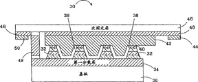
Figure 3 shows that second embodiment of a light-emitting diode of constructing according to the present invention 30, it utilizes flip-over type to install.As mentioned above, be to form little light-emitting diode 32 arrays by the semi-conducting material that a complete light emitting diode construction is removed in etching.Each little light-emitting diode 32 has one by two active layers that opposite doped layer surrounded.The configuration and the size of little light-emitting diode are similar to the above embodiments.Yet in this embodiment, each little light-emitting diode has into the side of certain angle, and its upper strata is narrower than its lower floor.As mentioned above, little light emitting diode matrix forms on first dispersion layer 34 that is formed on the substrate 36.One insulating barrier 38 covers the surface of little light-emitting diode and first dispersion layer between adjacent little light-emitting diode.On each little light-emitting diode 32, a hole is included in the insulating barrier as contact point 40 on.One second dispersion layer 42 covers whole little light emitting diode matrix to interconnect with last contact point 40.
In this flip-over type embodiment, the emission of the light of self-luminous diode 50 is main by substrate 36.Second dispersion layer 42 can be reflective so that can be reflected to the substrate 36 of light-emitting diode to the light of the direction emission of second dispersion layer 42 from little light-emitting diode 32.Preferably be based on AlGaInN and a p-type upper strata is arranged as second dispersion layer and each little light-emitting diode 32 with Al or Ag.Contact point 40 is preferably Pt, Pt/Au, Pd, Pd/Au, Ni/Au, NiO or NiO/Au on each.
Because little light-emitting diode of those isolation, this embodiment have strengthened the interaction of emission light and sidewall.The part that is arranged in second dispersion layer 42 between little light-emitting diode is as LEEs, its make light by little LED reflection to substrate.By this time fixed bed, this framework also makes the heating power of this new light-emitting diode chip for backlight unit spread out of better.
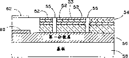
Fig. 4 and 5 is depicted as another embodiment of this new light-emitting diode 51, and this new light-emitting diode is an insulating barrier that separates first dispersion layer and second dispersion layer not.Little light-emitting diode 52 is that the conductive path by an interconnect grid 54 is connected with adjacent little light-emitting diode, wherein this path below semi-conducting material is arranged.Opening 55 in each grid 54 is a zone, the semi-conducting material at its place when making this light-emitting diode 51, from this light emitting diode construction by eating away.The residue of this structure is for 54 times little light-emitting diode 52 at this grid partly, and this slightly the grid path between the light-emitting diode be for 53 times semi-conducting material.Little light-emitting diode and the material under this path comprise an active layer by two opposite doped layers encirclements, and total then forms on one first dispersion layer 56 and a substrate 58.
One first make contact 60 that is deposited on first dispersion layer is applied to the lower floor of little light-emitting diode with electric current, and one be included in electric current and disperse second contact point 62 on the grid electric current to be distributed to the upper strata of little light-emitting diode.When applying one when being biased into this contact point 60 and 62, electric current be applied to this little light-emitting diode and under conductive path semi-conducting material, make them all luminous.Overflowing in the side of the little light LED material of light under those paths, has avoided total internal reflection.Therefore present technique can be common to any light emitting diode construction on any substrate and can realize with standard process techniques.
Make light-emitting diode 51 and at first will deposit first dispersion layer 56 on substrate 58, and then form a continuous light emitting diode construction, it covers electric current dispersion layer 56.Grid 54 is deposited on this light emitting diode construction, and the part that this light emitting diode construction can be seen in this grill openings can be come ablation by diverse ways, and for example wet chemical etch, reactive ion etching (RIE), ion grind or any other is used to remove the technology of semi-conducting material.Light emitting diode construction partly is also etched to provide a contact point 60 zones, and contact point 60 and 62 is deposited thereon.Grid 54 can be made by any electric conducting material, includes but not limited to metal, semimetal, semiconductor or its combination.Little light-emitting diode is preferably based on GaN, and the upper strata 55 of each little light-emitting diode is a p-type AlGaInN or its any alloy, and grid 54 is preferably made for example Ni, Pd, Au, Pt or its any combination with a thin metal.
Be shown in dotted line zone around little light-emitting diode one of them and this little light-emitting diode among Fig. 4, can comprise LEEs at its place and emit, below will narrate fully further to add high light.
Fig. 6 and 7 is depicted as two extra embodiment 70 and 80 of this new light-emitting diode, and it has different little light-emitting diodes and lattice structure 72 and 82, although also available many different structures.Each embodiment has one and else disperses contact point 73 and 83 down.In Fig. 6, little light-emitting diode 74 of this interconnection is distributed to each little light-emitting diode by different paths with the electric current intersection.Under every path, semi-conducting material is arranged so that itself and first dispersion layer are isolated.Grid 72 provides the opening that is the square array structure to interact with light.
In Fig. 7, little light-emitting diode is that randomness ground is shaped and has at random interconnection vias.In addition, under those paths, semi-conducting material is arranged.This random structure can reduce for the path number that TIR light is propagated before making wherein little light-emitting diode of TIR light in running into a grill openings wherein.As mentioned above, in Fig. 6 and 7,, below will narrate fully around the little light-emitting diode 76 of being shown in dotted line of little light-emitting diode and 86 and be looped around its peripheral LEEs.
Distance between opening size and the opening is preferably between 1 to the 30 μ m, but can be bigger or less.This opening can be aperiodic or periodic structure because the interaction of light and little light-emitting diodes tube edges does not need above arbitrary condition in itself.In preferred embodiment, the width of the grill openings on a p-type AlGaInN layer is between 1 micron to 20 microns, and the width of little light-emitting diode is then between 1 micron to 30 microns.
Three previous embodiment can combine with the LEEs between little light-emitting diode all further increases the light emission.This LEEs both can be on the side of little light-emitting diode, can form on the surface of first dispersion layer again, perhaps, then can not form on electrically-conductive backing plate in those do not have the embodiment of first dispersion layer.
Although can use other LEEs shape and the shape of protection scope of the present invention shown in also being not limited to, Fig. 8 still shows some alternative LEEs shapes, and those shapes comprise in an embodiment of the present invention.LEEs82,84,86 has curved surface, and LEEs 88,90,92,94 then has the linear surface of segmentation.In addition, this LEE can be an exasperate layer at random, and it can be as a light dispersion device.
LEEs available standards etching technique forms, wet chemical etch for example, and RIE, or ion grinds.In this preferred embodiment, LEEs is (for example a ultraviolet ray or the electron beam sensitive photoresistance) that forms by the polymer as an ablation etching mask that uses a commercialization.This polymer at first is deposited, and forms the structure on similar side limit.This polymer can be heated to a temperature, and forms a linear gradually or crooked shape as the edge of remelting as the glass so that this polymer.This polymer thickness, planform, heating-up temperature and heating time will determine this edge shape.This structure can be transformed into little light-emitting diode based on AlGaInN with RIE.Can make linear and curved LEEs easily with the method, and by using a plurality of etching masks linear LEEs of structural segmentation formula easily.
The second kind of technology that is used for forming LEEs is to use the negative polarity UV photoresistance that can expose.At first, make this photoresistance continue to expose a specific time for exposure, and it is processed to produce a negative polarity.This photoresistance is developed cut the bending or the linearity configuration at the end to produce one in its cross section.This structure can be transformed into semi-conducting material via a dry-etching technology then.For these two embodiment, the environment of dry-etching also can influence the net shape of lens in the semi-conducting material.
Fig. 9-15 is depicted as the embodiment of new light-emitting diode, and wherein LEEs combines to add high light with little light emitting diode matrix in various modes and emits.These embodiment explanation is according to some feasible occupation modes of LEEs of the present invention, and protection scope of the present invention and be not limited to described embodiment.
Figure 9 shows that one is similar to the new light-emitting diode 100 of the light-emitting diode 51 in Fig. 4 and 5, but it has LEEs 101,102,103 between little light-emitting diode 104.Those LEEs 101,102,103 can reflect away the light that is directed to the side of passing a little light-emitting diode from this LEEs, and light is directed to the shell again from this substrate.The light transmission TIR that interface between the substrate 108 and first dispersion layer 106 reflects away can also interact with LEEs 101,102,103 and escape into this shell so that the light output of the last one to be provided.Can be deposited on the new light-emitting diode at the LEEs described in Fig. 8, or be worked in the new light-emitting diode.As mentioned above, the thickness of LEE also can change, preferable thickness at 0.5 μ m in the scope of 10 μ m.
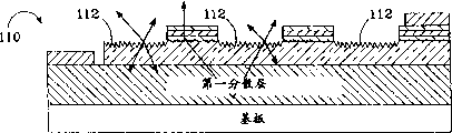
Figure 10 shows that a new light-emitting diode 110, it is similar to the light-emitting diode 100 of Fig. 9, but it has the disperse LEE 112 of exasperate at random between this little light-emitting diode 113.The interaction of light and rough layer makes TIR luminous energy with less than arriving at the surface under its critical angle, and overflows before being absorbed.In this preferred embodiment, form this matsurface in the semiconductor by using polystyrene or silica microsphere micro-roughness to be forwarded to as an etching mask.The thickness of random rough degree and width can be less than 20nm, or arrive 500nm more, and preferable size is approximately the light wavelength that light-emitting diode produces.
Figure 11 shows that a new light-emitting diode 120, it is similar to the light-emitting diode 110 of Figure 10, but it comprises a current blocked layer in this little light-emitting diode.This barrier layer 122 directs electric current under the disperse LEE 124, has increased the chance that light and LEE interact and overflow.
Selection as form LEEs between little light-emitting diode can make LEEs directly be formed on the side of little light-emitting diode.Figure 12 shows that a new light-emitting diode 130, it is similar to Fig. 9,10 and 11 light-emitting diode, but it has the different LEEs 131-133 on the side that directly is formed at each little light-emitting diode.This LEEs can utilize aforesaid identical method to form.The light of propagating to little led sides is altered course so that light is overflowed by first dispersion layer 135 or little light-emitting diode 132 from the wherein one side of substrate 134.Because those LEEs on little light-emitting diodes tube edge also make the effusion chance of the light that reflects from substrate 134 increase.
Figure 13 shows that a new light-emitting diode 140, it has the LEEs 142 of the curved surface on the side that is formed at little light-emitting diode 144.This curved surface LEE 142 has extra benefit, and it makes the light of light-emitting diode focus on a clearer and more definite direction.The thickness of LEEs 142 and width can change along with the preferred thickness of any one LEE, and this preferred thickness is that 0.1 μ m is to 50 μ m.
Figure 14 and 15 is depicted as two extra embodiment.Figure 14 shows that a new light-emitting diode 150, it is at LEEs 152 that a composite surface is arranged on the side of little light-emitting diode 154 and LEEs 156 that complete curved surface is arranged between this little light-emitting diode 154.Those LEEs actings in conjunction make light refraction and reflection pass the overflow shell of this light-emitting diode of substrate and add high light and emit.
Figure 15 shows that new light-emitting diode 160, its use is similar to the concrete flip-over type of embodiment shown in Figure 3 and installs.It has curved surface LEEs 162 on the side of little light-emitting diode 164.This second dispersion layer 164 is reflective and this substrate 166 is main emitting surface.The part acting in conjunction of the LEEs 162 and second dispersion layer 164, the shell that makes light refraction and reflection pass substrate effusion light-emitting diode adds high light and emits.
Though the present invention has made quite detailed narration according to its some preferable configurations, other modification also is possible.For instance, the lower floor of the little light-emitting diode in little light emitting diode matrix can connect.Employed smooth discharging structure also can be done many different combinations and many different shapes and size are arranged.Simultaneously, described light emitting diode construction can have the active layer that is clipped between the opposite doped layer more than.Therefore, spirit of claims of the present invention and protection range are not limited to its described preferred embodiment.
Claims (10)
1. one kind has and adds the light-emitting diode that high light is emitted, and it is characterized in that it comprises:
First dispersion layer (20) of one conduction;
A plurality of little light-emitting diodes (12) are deposited on the surface of described first dispersion layer (20) respectively, and each described little light-emitting diode all comprises:
One p-type layer (16);
One n-type layer (18);
One active layer (14), it is clipped between described p-type and the n-type layer (16,18), and wherein said p-type or n-type layer are a upper strata, and in addition one deck then is a lower floor, is distributed to described lower floor from the electric current of described first dispersion layer (20);
One second dispersion layer (24), it is on described little light-emitting diode (12), electric current from described second dispersion layer (24) is distributed to described upper strata, applies a bias voltage to described first and second dispersion layer (20,24) and can make described little light-emitting diode (12) luminous.
2. light-emitting diode according to claim 1 is characterized in that it further comprises a substrate (28), this substrate and described first dispersion layer (20) with described little light-emitting diode (12) opposite surfaces adjacency.
3. light-emitting diode according to claim 1, it is characterized in that it further comprises an insulating barrier (23), the surface that this insulating barrier covers described little light-emitting diode (12) and is positioned at described first dispersion layer (20) between described little light-emitting diode (12), described insulating barrier (23) are deposited between described second dispersion layer (24) and the described little light-emitting diode (12).
4. light-emitting diode according to claim 3 is characterized in that described insulating barrier (23) is equipped with the hole on each described little light-emitting diode (12), and described second dispersion layer (24) contacts by the described little light-emitting diode of this hole and each (12).
5. light-emitting diode according to claim 4, it is characterized in that described second dispersion layer (24) is the electric current dispersion grid of an interconnection, it has the conductive path of a plurality of interconnection, each described little light-emitting diode (12) all has one or more conductive paths on it, and sees through described hole and contact with described upper strata.
6. light-emitting diode according to claim 1, it is characterized in that it further comprises light and emits assembly (82,84,86,88,90,92,94), it combines with described little light-emitting diode (12) interacting with the light of overflowing from little light-emitting diode (12), thereby further strengthens the light of emitting from described light-emitting diode.
7. light-emitting diode according to claim 6 is characterized in that it is to be deposited on the surface of described first dispersion layer (106) and between described little light-emitting diode (104) that described light is emitted assembly (101,102,103).
8. light-emitting diode according to claim 4, it is characterized in that described second dispersion layer (42) is a reflective metal layer, it is deposited on this little light-emitting diode (32), described light-emitting diode further comprises substrate (36), this substrate and described first dispersion layer (34) with described little light-emitting diode (32) opposite surfaces adjacency, and one with the affixed inferior fixed bed (46) of described metal level (42), the described substrate (36) of described light-emitting diode becomes main light-emitting area.
9. light-emitting diode according to claim 8, it is characterized in that it further comprises a conduction finger (49), this finger is positioned between described fixed bed (46) and described first dispersion layer (34), one first make contact (50) on described fixed bed (46) is connected with described conduction finger (49), and one second contact point (44) on described fixed bed (46) be connected with described metal level (48), described little light-emitting diode (32) is applied in described contact point (44 at a bias voltage, 50) time, promptly luminous.
10. light-emitting diode is characterized in that it comprises:
One first dispersion layer (56);
One little light-emitting diode (52) array, it is deposited on described first dispersion layer (56), and an electric current that puts on described first dispersion layer (56) is distributed to described little light-emitting diode (52);
The electric current of one interconnection disperses grid (54) to be deposited on described little light-emitting diode (52), described grid is provided with conductive path (53) between described little light-emitting diode (52), an electric current that puts on described grid (54) is distributed to described little light-emitting diode (52);
Semi-conducting material, it is positioned under the described conductive path (53) between little light-emitting diode (52), and described semi-conducting material makes described first dispersion layer (56) and described conductive path (53) electric insulation;
Lay respectively at first and second contact point (60,62) on described first and second dispersion layer (56,54), apply a bias voltage to described contact point (60,62) and can make described little light-emitting diode (52) array light-emitting.
Applications Claiming Priority (4)
| Application Number | Priority Date | Filing Date | Title |
|---|---|---|---|
| US16881799P | 1999-12-03 | 1999-12-03 | |
| US60/168,817 | 1999-12-03 | ||
| US09/713,576 | 2000-11-14 | ||
| US09/713,576 US6410942B1 (en) | 1999-12-03 | 2000-11-14 | Enhanced light extraction through the use of micro-LED arrays |
Publications (2)
| Publication Number | Publication Date |
|---|---|
| CN1402880A CN1402880A (en) | 2003-03-12 |
| CN1229871C true CN1229871C (en) | 2005-11-30 |
Family
ID=26864480
Family Applications (1)
| Application Number | Title | Priority Date | Filing Date |
|---|---|---|---|
| CNB008166013A Expired - Lifetime CN1229871C (en) | 1999-12-03 | 2000-11-20 | Micro-LED arrays with enhanced light extraction |
Country Status (9)
| Country | Link |
|---|---|
| US (1) | US6410942B1 (en) |
| EP (3) | EP1234334B1 (en) |
| JP (1) | JP5511114B2 (en) |
| KR (1) | KR100731673B1 (en) |
| CN (1) | CN1229871C (en) |
| AU (1) | AU1790501A (en) |
| CA (1) | CA2393007C (en) |
| HK (1) | HK1048707A1 (en) |
| WO (1) | WO2001041219A1 (en) |
Cited By (1)
| Publication number | Priority date | Publication date | Assignee | Title |
|---|---|---|---|---|
| CN103312412A (en) * | 2012-03-06 | 2013-09-18 | 财团法人工业技术研究院 | Visible light communication transceiver and system |
Families Citing this family (355)
| Publication number | Priority date | Publication date | Assignee | Title |
|---|---|---|---|---|
| US6657236B1 (en) | 1999-12-03 | 2003-12-02 | Cree Lighting Company | Enhanced light extraction in LEDs through the use of internal and external optical elements |
| US20020017652A1 (en) * | 2000-08-08 | 2002-02-14 | Stefan Illek | Semiconductor chip for optoelectronics |
| US7547921B2 (en) * | 2000-08-08 | 2009-06-16 | Osram Opto Semiconductors Gmbh | Semiconductor chip for optoelectronics |
| US7053419B1 (en) | 2000-09-12 | 2006-05-30 | Lumileds Lighting U.S., Llc | Light emitting diodes with improved light extraction efficiency |
| JP2002141556A (en) | 2000-09-12 | 2002-05-17 | Lumileds Lighting Us Llc | Light emitting diode with improved light extraction efficiency |
| US7064355B2 (en) | 2000-09-12 | 2006-06-20 | Lumileds Lighting U.S., Llc | Light emitting diodes with improved light extraction efficiency |
| JP2002198560A (en) * | 2000-12-26 | 2002-07-12 | Sharp Corp | Semiconductor light emitting element and its manufacturing method |
| US6791119B2 (en) * | 2001-02-01 | 2004-09-14 | Cree, Inc. | Light emitting diodes including modifications for light extraction |
| JP4724924B2 (en) * | 2001-02-08 | 2011-07-13 | ソニー株式会社 | Manufacturing method of display device |
| US6746889B1 (en) * | 2001-03-27 | 2004-06-08 | Emcore Corporation | Optoelectronic device with improved light extraction |
| JP2002344011A (en) * | 2001-05-15 | 2002-11-29 | Sony Corp | Display element and display unit using the same |
| US6897704B2 (en) * | 2001-05-25 | 2005-05-24 | Thunder Creative Technologies, Inc. | Electronic isolator |
| TW583348B (en) * | 2001-06-19 | 2004-04-11 | Phoenix Prec Technology Corp | A method for electroplating Ni/Au layer substrate without using electroplating wire |
| JP4055503B2 (en) | 2001-07-24 | 2008-03-05 | 日亜化学工業株式会社 | Semiconductor light emitting device |
| WO2003026355A2 (en) * | 2001-08-30 | 2003-03-27 | Osram Opto Semiconductors Gmbh | Electroluminescent body |
| TW523939B (en) * | 2001-11-07 | 2003-03-11 | Nat Univ Chung Hsing | High-efficient light emitting diode and its manufacturing method |
| US6881983B2 (en) * | 2002-02-25 | 2005-04-19 | Kopin Corporation | Efficient light emitting diodes and lasers |
| JP3776824B2 (en) | 2002-04-05 | 2006-05-17 | 株式会社東芝 | Semiconductor light emitting device and manufacturing method thereof |
| US20030189215A1 (en) | 2002-04-09 | 2003-10-09 | Jong-Lam Lee | Method of fabricating vertical structure leds |
| JP4585014B2 (en) * | 2002-04-12 | 2010-11-24 | ソウル セミコンダクター カンパニー リミテッド | Light emitting device |
| US20060175625A1 (en) * | 2002-05-28 | 2006-08-10 | Ryoji Yokotani | Light emitting element, lighting device and surface emission illuminating device using it |
| US6841802B2 (en) * | 2002-06-26 | 2005-01-11 | Oriol, Inc. | Thin film light emitting diode |
| US6955985B2 (en) * | 2002-06-28 | 2005-10-18 | Kopin Corporation | Domain epitaxy for thin film growth |
| DE10234977A1 (en) * | 2002-07-31 | 2004-02-12 | Osram Opto Semiconductors Gmbh | Radiation-emitting thin layer semiconductor component comprises a multiple layer structure based on gallium nitride containing an active radiation-producing layer and having a first main surface and a second main surface |
| KR101052139B1 (en) * | 2002-08-01 | 2011-07-26 | 니치아 카가쿠 고교 가부시키가이샤 | Semiconductor light-emitting device, method for manufacturing same and light-emitting apparatus using same |
| KR20040013998A (en) * | 2002-08-09 | 2004-02-14 | 엘지전자 주식회사 | Fabrication method for led of limit exterior |
| EP1892764B1 (en) | 2002-08-29 | 2016-03-09 | Seoul Semiconductor Co., Ltd. | Light-emitting device having light-emitting diodes |
| JP3956918B2 (en) | 2002-10-03 | 2007-08-08 | 日亜化学工業株式会社 | Light emitting diode |
| US7071494B2 (en) * | 2002-12-11 | 2006-07-04 | Lumileds Lighting U.S. Llc | Light emitting device with enhanced optical scattering |
| JP2006512781A (en) * | 2002-12-30 | 2006-04-13 | オスラム オプト セミコンダクターズ ゲゼルシャフト ミット ベシュレンクテル ハフツング | Method for roughening surface of body and optoelectronic device |
| US7042020B2 (en) * | 2003-02-14 | 2006-05-09 | Cree, Inc. | Light emitting device incorporating a luminescent material |
| KR100964399B1 (en) * | 2003-03-08 | 2010-06-17 | 삼성전자주식회사 | Semiconductor laser diode and semiconductor laser diode assembly adopting the same |
| US7083993B2 (en) * | 2003-04-15 | 2006-08-01 | Luminus Devices, Inc. | Methods of making multi-layer light emitting devices |
| US7105861B2 (en) * | 2003-04-15 | 2006-09-12 | Luminus Devices, Inc. | Electronic device contact structures |
| US7262550B2 (en) * | 2003-04-15 | 2007-08-28 | Luminus Devices, Inc. | Light emitting diode utilizing a physical pattern |
| US7166871B2 (en) * | 2003-04-15 | 2007-01-23 | Luminus Devices, Inc. | Light emitting systems |
| US7667238B2 (en) * | 2003-04-15 | 2010-02-23 | Luminus Devices, Inc. | Light emitting devices for liquid crystal displays |
| US7074631B2 (en) * | 2003-04-15 | 2006-07-11 | Luminus Devices, Inc. | Light emitting device methods |
| US7521854B2 (en) * | 2003-04-15 | 2009-04-21 | Luminus Devices, Inc. | Patterned light emitting devices and extraction efficiencies related to the same |
| US6831302B2 (en) | 2003-04-15 | 2004-12-14 | Luminus Devices, Inc. | Light emitting devices with improved extraction efficiency |
| US7084434B2 (en) * | 2003-04-15 | 2006-08-01 | Luminus Devices, Inc. | Uniform color phosphor-coated light-emitting diode |
| US7098589B2 (en) * | 2003-04-15 | 2006-08-29 | Luminus Devices, Inc. | Light emitting devices with high light collimation |
| US7211831B2 (en) * | 2003-04-15 | 2007-05-01 | Luminus Devices, Inc. | Light emitting device with patterned surfaces |
| US20040259279A1 (en) * | 2003-04-15 | 2004-12-23 | Erchak Alexei A. | Light emitting device methods |
| US7274043B2 (en) * | 2003-04-15 | 2007-09-25 | Luminus Devices, Inc. | Light emitting diode systems |
| KR101148332B1 (en) * | 2003-04-30 | 2012-05-25 | 크리, 인코포레이티드 | High powered light emitter packages with compact optics |
| US7005679B2 (en) | 2003-05-01 | 2006-02-28 | Cree, Inc. | Multiple component solid state white light |
| ATE474332T1 (en) * | 2003-05-02 | 2010-07-15 | Univ College Cork Nat Univ Ie | LIGHT-EMITTING MEASUREMENT STRUCTURES WITH HIGH HEIGHT-TO-WIDTH RATIO AND QUASI-PARABOLIC SIDEWALLS AND PRODUCTION THEREOF |
| US6885034B1 (en) | 2003-05-09 | 2005-04-26 | Winston Vaughan Schoenfeld | Light emitting diode having multiple pits |
| US7122841B2 (en) | 2003-06-04 | 2006-10-17 | Kopin Corporation | Bonding pad for gallium nitride-based light-emitting devices |
| US20050000913A1 (en) * | 2003-07-03 | 2005-01-06 | Mark Betterly | Fluid treatment system |
| US7009213B2 (en) | 2003-07-31 | 2006-03-07 | Lumileds Lighting U.S., Llc | Light emitting devices with improved light extraction efficiency |
| EP1652238B1 (en) * | 2003-08-08 | 2010-10-27 | Kang, Sang-kyu | Nitride micro light emitting diode with high brightness and method of manufacturing the same |
| EP3699963A1 (en) * | 2003-08-19 | 2020-08-26 | Nichia Corporation | Semiconductor light emitting diode and method of manufacturing its substrate |
| US7344903B2 (en) * | 2003-09-17 | 2008-03-18 | Luminus Devices, Inc. | Light emitting device processes |
| US7341880B2 (en) * | 2003-09-17 | 2008-03-11 | Luminus Devices, Inc. | Light emitting device processes |
| US7915085B2 (en) | 2003-09-18 | 2011-03-29 | Cree, Inc. | Molded chip fabrication method |
| JP4881003B2 (en) * | 2003-09-26 | 2012-02-22 | オスラム オプト セミコンダクターズ ゲゼルシャフト ミット ベシュレンクテル ハフツング | Thin film semiconductor chip that emits radiation |
| EP1697983B1 (en) | 2003-12-09 | 2012-06-13 | The Regents of The University of California | Highly efficient gallium nitride based light emitting diodes having surface roughening |
| US7450311B2 (en) | 2003-12-12 | 2008-11-11 | Luminus Devices, Inc. | Optical display systems and methods |
| JP2005191099A (en) * | 2003-12-24 | 2005-07-14 | ▲さん▼圓光電股▲ふん▼有限公司 | Light-emitting diode device |
| US20050179046A1 (en) * | 2004-02-13 | 2005-08-18 | Kopin Corporation | P-type electrodes in gallium nitride-based light-emitting devices |
| US20050179042A1 (en) * | 2004-02-13 | 2005-08-18 | Kopin Corporation | Monolithic integration and enhanced light extraction in gallium nitride-based light-emitting devices |
| TWM271252U (en) * | 2004-12-14 | 2005-07-21 | Niching Ind Corp | Package structure of light-emitting device |
| JP2005259891A (en) * | 2004-03-10 | 2005-09-22 | Toyoda Gosei Co Ltd | Light emitting device |
| US7202141B2 (en) * | 2004-03-29 | 2007-04-10 | J.P. Sercel Associates, Inc. | Method of separating layers of material |
| US7419912B2 (en) * | 2004-04-01 | 2008-09-02 | Cree, Inc. | Laser patterning of light emitting devices |
| US7064356B2 (en) * | 2004-04-16 | 2006-06-20 | Gelcore, Llc | Flip chip light emitting diode with micromesas and a conductive mesh |
| US7795623B2 (en) * | 2004-06-30 | 2010-09-14 | Cree, Inc. | Light emitting devices having current reducing structures and methods of forming light emitting devices having current reducing structures |
| US7534633B2 (en) * | 2004-07-02 | 2009-05-19 | Cree, Inc. | LED with substrate modifications for enhanced light extraction and method of making same |
| US20090023239A1 (en) * | 2004-07-22 | 2009-01-22 | Luminus Devices, Inc. | Light emitting device processes |
| US20060038188A1 (en) | 2004-08-20 | 2006-02-23 | Erchak Alexei A | Light emitting diode systems |
| US20060049418A1 (en) * | 2004-09-03 | 2006-03-09 | Tzi-Chi Wen | Epitaxial structure and fabrication method of nitride semiconductor device |
| US7737459B2 (en) * | 2004-09-22 | 2010-06-15 | Cree, Inc. | High output group III nitride light emitting diodes |
| US7259402B2 (en) * | 2004-09-22 | 2007-08-21 | Cree, Inc. | High efficiency group III nitride-silicon carbide light emitting diode |
| US8513686B2 (en) * | 2004-09-22 | 2013-08-20 | Cree, Inc. | High output small area group III nitride LEDs |
| US8174037B2 (en) | 2004-09-22 | 2012-05-08 | Cree, Inc. | High efficiency group III nitride LED with lenticular surface |
| US7352006B2 (en) * | 2004-09-28 | 2008-04-01 | Goldeneye, Inc. | Light emitting diodes exhibiting both high reflectivity and high light extraction |
| US7404756B2 (en) | 2004-10-29 | 2008-07-29 | 3M Innovative Properties Company | Process for manufacturing optical and semiconductor elements |
| US20060091411A1 (en) | 2004-10-29 | 2006-05-04 | Ouderkirk Andrew J | High brightness LED package |
| US7329982B2 (en) | 2004-10-29 | 2008-02-12 | 3M Innovative Properties Company | LED package with non-bonded optical element |
| US7462502B2 (en) | 2004-11-12 | 2008-12-09 | Philips Lumileds Lighting Company, Llc | Color control by alteration of wavelength converting element |
| US7419839B2 (en) | 2004-11-12 | 2008-09-02 | Philips Lumileds Lighting Company, Llc | Bonding an optical element to a light emitting device |
| JP2006147679A (en) * | 2004-11-17 | 2006-06-08 | Sony Corp | Integrated light emitting diode, manufacturing method thereof, display and lighting apparatus for light emitting diode |
| US7304363B1 (en) | 2004-11-26 | 2007-12-04 | United States Of America As Represented By The Secretary Of The Army | Interacting current spreader and junction extender to increase the voltage blocked in the off state of a high power semiconductor device |
| US20060124943A1 (en) * | 2004-12-14 | 2006-06-15 | Elite Optoelectronics Inc. | Large-sized light-emitting diodes with improved light extraction efficiency |
| US8288942B2 (en) | 2004-12-28 | 2012-10-16 | Cree, Inc. | High efficacy white LED |
| KR101138974B1 (en) * | 2005-01-07 | 2012-04-25 | 서울옵토디바이스주식회사 | Luminous element and method of manufacturing thereof |
| JP4687109B2 (en) * | 2005-01-07 | 2011-05-25 | ソニー株式会社 | Manufacturing method of integrated light emitting diode |
| US7524686B2 (en) * | 2005-01-11 | 2009-04-28 | Semileds Corporation | Method of making light emitting diodes (LEDs) with improved light extraction by roughening |
| US7186580B2 (en) * | 2005-01-11 | 2007-03-06 | Semileds Corporation | Light emitting diodes (LEDs) with improved light extraction by roughening |
| US20060154393A1 (en) * | 2005-01-11 | 2006-07-13 | Doan Trung T | Systems and methods for removing operating heat from a light emitting diode |
| US20060151801A1 (en) * | 2005-01-11 | 2006-07-13 | Doan Trung T | Light emitting diode with thermo-electric cooler |
| US7692207B2 (en) * | 2005-01-21 | 2010-04-06 | Luminus Devices, Inc. | Packaging designs for LEDs |
| US7170100B2 (en) | 2005-01-21 | 2007-01-30 | Luminus Devices, Inc. | Packaging designs for LEDs |
| US7335920B2 (en) | 2005-01-24 | 2008-02-26 | Cree, Inc. | LED with current confinement structure and surface roughening |
| KR101138944B1 (en) * | 2005-01-26 | 2012-04-25 | 서울옵토디바이스주식회사 | Light emitting device having a plurality of light emitting cells connected in series and method of fabricating the same |
| US7535028B2 (en) * | 2005-02-03 | 2009-05-19 | Ac Led Lighting, L.Lc. | Micro-LED based high voltage AC/DC indicator lamp |
| JP2006261659A (en) * | 2005-02-18 | 2006-09-28 | Sumitomo Chemical Co Ltd | Manufacturing method for semiconductor light emitting device |
| US7932111B2 (en) | 2005-02-23 | 2011-04-26 | Cree, Inc. | Substrate removal process for high light extraction LEDs |
| US20060204865A1 (en) * | 2005-03-08 | 2006-09-14 | Luminus Devices, Inc. | Patterned light-emitting devices |
| US20070045640A1 (en) * | 2005-08-23 | 2007-03-01 | Erchak Alexei A | Light emitting devices for liquid crystal displays |
| US8163575B2 (en) * | 2005-06-17 | 2012-04-24 | Philips Lumileds Lighting Company Llc | Grown photonic crystals in semiconductor light emitting devices |
| KR100599012B1 (en) | 2005-06-29 | 2006-07-12 | 서울옵토디바이스주식회사 | Light emitting diode having a thermal conductive substrate and method of fabricating the same |
| US20090179211A1 (en) * | 2005-07-14 | 2009-07-16 | Tae-Kyung Yoo | Light emitting device |
| US20070018182A1 (en) * | 2005-07-20 | 2007-01-25 | Goldeneye, Inc. | Light emitting diodes with improved light extraction and reflectivity |
| US8674375B2 (en) * | 2005-07-21 | 2014-03-18 | Cree, Inc. | Roughened high refractive index layer/LED for high light extraction |
| US7391059B2 (en) * | 2005-10-17 | 2008-06-24 | Luminus Devices, Inc. | Isotropic collimation devices and related methods |
| US20070085098A1 (en) * | 2005-10-17 | 2007-04-19 | Luminus Devices, Inc. | Patterned devices and related methods |
| US7348603B2 (en) * | 2005-10-17 | 2008-03-25 | Luminus Devices, Inc. | Anisotropic collimation devices and related methods |
| US7388233B2 (en) * | 2005-10-17 | 2008-06-17 | Luminus Devices, Inc. | Patchwork patterned devices and related methods |
| US20080099777A1 (en) * | 2005-10-19 | 2008-05-01 | Luminus Devices, Inc. | Light-emitting devices and related systems |
| KR100779078B1 (en) * | 2005-12-09 | 2007-11-27 | 한국전자통신연구원 | Silicon-based light emitting diode for enhancing light extraction efficiency and fabrication method thereof |
| JP4908837B2 (en) * | 2005-12-13 | 2012-04-04 | キヤノン株式会社 | Light emitting element array and image forming apparatus |
| EP1969633B1 (en) | 2005-12-22 | 2018-08-29 | Cree, Inc. | Lighting device |
| US7772604B2 (en) | 2006-01-05 | 2010-08-10 | Illumitex | Separate optical device for directing light from an LED |
| JP2007214260A (en) * | 2006-02-08 | 2007-08-23 | Matsushita Electric Ind Co Ltd | Semiconductor light emitting element and its process for fabrication |
| KR20070088145A (en) * | 2006-02-24 | 2007-08-29 | 엘지전자 주식회사 | Light emitting diode and fabricating method thereof |
| US8008676B2 (en) | 2006-05-26 | 2011-08-30 | Cree, Inc. | Solid state light emitting device and method of making same |
| KR20140116536A (en) | 2006-05-31 | 2014-10-02 | 크리, 인코포레이티드 | Lighting device and method of lighting |
| KR100759896B1 (en) * | 2006-06-15 | 2007-09-18 | 삼성전자주식회사 | Backlight module stacked at least one luminescence element and fabrication thereof |
| US7674639B2 (en) * | 2006-08-14 | 2010-03-09 | Bridgelux, Inc | GaN based LED with etched exposed surface for improved light extraction efficiency and method for making the same |
| CN101554089A (en) * | 2006-08-23 | 2009-10-07 | 科锐Led照明科技公司 | Lighting device and lighting method |
| US20100224890A1 (en) * | 2006-09-18 | 2010-09-09 | Cree, Inc. | Light emitting diode chip with electrical insulation element |
| US8087960B2 (en) | 2006-10-02 | 2012-01-03 | Illumitex, Inc. | LED system and method |
| US20090275157A1 (en) * | 2006-10-02 | 2009-11-05 | Illumitex, Inc. | Optical device shaping |
| US20080087875A1 (en) * | 2006-10-11 | 2008-04-17 | Feng-Hsu Fan | Protection for the epitaxial structure of metal devices |
| US9318327B2 (en) | 2006-11-28 | 2016-04-19 | Cree, Inc. | Semiconductor devices having low threading dislocations and improved light extraction and methods of making the same |
| EP2095011A1 (en) | 2006-12-04 | 2009-09-02 | Cree Led Lighting Solutions, Inc. | Lighting assembly and lighting method |
| CN101622493A (en) * | 2006-12-04 | 2010-01-06 | 科锐Led照明科技公司 | Lighting device and lighting method |
| US8110838B2 (en) * | 2006-12-08 | 2012-02-07 | Luminus Devices, Inc. | Spatial localization of light-generating portions in LEDs |
| EP3848970A1 (en) * | 2007-01-22 | 2021-07-14 | Cree, Inc. | Multiple light emitting diode emitter |
| TW200837943A (en) * | 2007-01-22 | 2008-09-16 | Led Lighting Fixtures Inc | Fault tolerant light emitters, systems incorporating fault tolerant light emitters and methods of fabricating fault tolerant light emitters |
| US8110425B2 (en) | 2007-03-20 | 2012-02-07 | Luminus Devices, Inc. | Laser liftoff structure and related methods |
| KR100849826B1 (en) | 2007-03-29 | 2008-07-31 | 삼성전기주식회사 | Light emitting device and package including the same |
| WO2009012287A1 (en) * | 2007-07-17 | 2009-01-22 | Cree Led Lighting Solutions, Inc. | Optical elements with internal optical features and methods of fabricating same |
| US8617997B2 (en) * | 2007-08-21 | 2013-12-31 | Cree, Inc. | Selective wet etching of gold-tin based solder |
| US11114594B2 (en) * | 2007-08-24 | 2021-09-07 | Creeled, Inc. | Light emitting device packages using light scattering particles of different size |
| US8368100B2 (en) * | 2007-11-14 | 2013-02-05 | Cree, Inc. | Semiconductor light emitting diodes having reflective structures and methods of fabricating same |
| US9431589B2 (en) * | 2007-12-14 | 2016-08-30 | Cree, Inc. | Textured encapsulant surface in LED packages |
| DE102008019902A1 (en) * | 2007-12-21 | 2009-06-25 | Osram Opto Semiconductors Gmbh | Optoelectronic component and production method for an optoelectronic component |
| DE102008003182A1 (en) * | 2008-01-04 | 2009-07-09 | Osram Opto Semiconductors Gmbh | Optoelectronic component |
| JP2011512037A (en) | 2008-02-08 | 2011-04-14 | イルミテックス, インコーポレイテッド | System and method for emitter layer shaping |
| JP5094535B2 (en) * | 2008-05-07 | 2012-12-12 | 富士フイルム株式会社 | Recess formation method, uneven product manufacturing method, light emitting element manufacturing method, and optical element manufacturing method |
| WO2009152237A1 (en) * | 2008-06-11 | 2009-12-17 | Susanne Gardner | Beverages composed of wine components |
| US7939839B2 (en) * | 2008-09-11 | 2011-05-10 | Bridgelux, Inc. | Series connected segmented LED |
| US7825427B2 (en) * | 2008-09-12 | 2010-11-02 | Bridgelux, Inc. | Method and apparatus for generating phosphor film with textured surface |
| US9051177B2 (en) * | 2008-10-27 | 2015-06-09 | The United States Of America As Represented By The Secretary Of The Army | Active optical limiting semiconductor device and method with active region transparent to light becoming opaque when not biased |
| TWI375338B (en) * | 2008-11-27 | 2012-10-21 | Epistar Corp | Opto-electronic device |
| TW201034256A (en) | 2008-12-11 | 2010-09-16 | Illumitex Inc | Systems and methods for packaging light-emitting diode devices |
| TWI418060B (en) * | 2008-12-26 | 2013-12-01 | Lextar Electronics Corp | Method for fabricating light emitting diode chip |
| US7982409B2 (en) | 2009-02-26 | 2011-07-19 | Bridgelux, Inc. | Light sources utilizing segmented LEDs to compensate for manufacturing variations in the light output of individual segmented LEDs |
| KR101134810B1 (en) * | 2009-03-03 | 2012-04-13 | 엘지이노텍 주식회사 | Light emitting device and method for fabricating the same |
| JP5196403B2 (en) * | 2009-03-23 | 2013-05-15 | 国立大学法人山口大学 | Method for manufacturing sapphire substrate and semiconductor device |
| US8585253B2 (en) | 2009-08-20 | 2013-11-19 | Illumitex, Inc. | System and method for color mixing lens array |
| US8449128B2 (en) | 2009-08-20 | 2013-05-28 | Illumitex, Inc. | System and method for a lens and phosphor layer |
| KR20110043282A (en) * | 2009-10-21 | 2011-04-27 | 엘지이노텍 주식회사 | Light emitting device and method for fabricating the same |
| KR101039931B1 (en) * | 2009-10-21 | 2011-06-09 | 엘지이노텍 주식회사 | Light emitting device and method for fabricating the same |
| US8783915B2 (en) | 2010-02-11 | 2014-07-22 | Bridgelux, Inc. | Surface-textured encapsulations for use with light emitting diodes |
| US8338317B2 (en) | 2011-04-06 | 2012-12-25 | Infineon Technologies Ag | Method for processing a semiconductor wafer or die, and particle deposition device |
| KR100999733B1 (en) * | 2010-02-18 | 2010-12-08 | 엘지이노텍 주식회사 | Light emitting device, method for fabricating the light emitting device and light emitting device package |
| KR101601624B1 (en) * | 2010-02-19 | 2016-03-09 | 삼성전자주식회사 | Semiconductor light emitting device having a multi-cell array, light emitting module and illumination apparatus |
| TWI485884B (en) * | 2010-03-30 | 2015-05-21 | Advanced Optoelectronic Tech | Light-emitting diode and method for manufacturing the same |
| US8329482B2 (en) | 2010-04-30 | 2012-12-11 | Cree, Inc. | White-emitting LED chips and method for making same |
| KR20110132136A (en) * | 2010-06-01 | 2011-12-07 | 삼성전자주식회사 | Light emitting device using connection structure and manufacturing method of the same |
| US8193546B2 (en) * | 2010-06-04 | 2012-06-05 | Pinecone Energies, Inc. | Light-emitting-diode array with polymer between light emitting devices |
| WO2012014758A1 (en) * | 2010-07-26 | 2012-02-02 | Semiconductor Energy Laboratory Co., Ltd. | Light-emitting device and lighting device |
| US9070851B2 (en) | 2010-09-24 | 2015-06-30 | Seoul Semiconductor Co., Ltd. | Wafer-level light emitting diode package and method of fabricating the same |
| US9899329B2 (en) | 2010-11-23 | 2018-02-20 | X-Celeprint Limited | Interconnection structures and methods for transfer-printed integrated circuit elements with improved interconnection alignment tolerance |
| JP5589812B2 (en) | 2010-12-06 | 2014-09-17 | 豊田合成株式会社 | Semiconductor light emitting device |
| US9166126B2 (en) | 2011-01-31 | 2015-10-20 | Cree, Inc. | Conformally coated light emitting devices and methods for providing the same |
| TWI467805B (en) * | 2011-03-08 | 2015-01-01 | Opto Tech Corp | Light emitting diode having large viewing angle and method of fabricating thereof |
| KR101106139B1 (en) * | 2011-04-04 | 2012-01-20 | 서울옵토디바이스주식회사 | Light emitting diode with a metal reflection layer expanded and method for manufacturing the same |
| KR101115538B1 (en) * | 2011-04-04 | 2012-02-28 | 서울옵토디바이스주식회사 | Luminous device and the method therefor |
| US20120261686A1 (en) * | 2011-04-12 | 2012-10-18 | Lu Chi Wei | Light-emitting element and the manufacturing method thereof |
| KR101737981B1 (en) | 2011-05-17 | 2017-05-22 | 한국전자통신연구원 | GAlIUM-NITRIDE LIGHT EMITTING DEVICE OF MICROARRAY TYPE STRUCTURE AND MANUFACTURING THEREOF |
| US8934259B2 (en) | 2011-06-08 | 2015-01-13 | Semprius, Inc. | Substrates with transferable chiplets |
| KR101221336B1 (en) * | 2011-07-12 | 2013-01-21 | 서울옵토디바이스주식회사 | Light emitting device and method of fabricating the same |
| US8957440B2 (en) | 2011-10-04 | 2015-02-17 | Cree, Inc. | Light emitting devices with low packaging factor |
| KR101901589B1 (en) * | 2011-11-14 | 2018-09-27 | 엘지이노텍 주식회사 | Light emitting device |
| US8794501B2 (en) | 2011-11-18 | 2014-08-05 | LuxVue Technology Corporation | Method of transferring a light emitting diode |
| US8349116B1 (en) | 2011-11-18 | 2013-01-08 | LuxVue Technology Corporation | Micro device transfer head heater assembly and method of transferring a micro device |
| US8573469B2 (en) | 2011-11-18 | 2013-11-05 | LuxVue Technology Corporation | Method of forming a micro LED structure and array of micro LED structures with an electrically insulating layer |
| US9620478B2 (en) | 2011-11-18 | 2017-04-11 | Apple Inc. | Method of fabricating a micro device transfer head |
| KR101337613B1 (en) * | 2011-12-06 | 2013-12-06 | 서울바이오시스 주식회사 | Luminous device and the method therefor |
| JP2015507370A (en) | 2012-02-02 | 2015-03-05 | ザ プロクター アンド ギャンブルカンパニー | Luminescent laminate and method for producing the same |
| WO2013117760A1 (en) * | 2012-02-10 | 2013-08-15 | University College Cork, National University Of Ireland, Cork | Light emitting diode chip |
| GB201215632D0 (en) | 2012-09-03 | 2012-10-17 | Infiniled Ltd | Optical device |
| JP5462333B1 (en) | 2012-09-21 | 2014-04-02 | 株式会社東芝 | Semiconductor light emitting device and manufacturing method thereof |
| DE102012109460B4 (en) * | 2012-10-04 | 2024-03-07 | OSRAM Opto Semiconductors Gesellschaft mit beschränkter Haftung | Method for producing a light-emitting diode display and light-emitting diode display |
| JP2016503516A (en) * | 2012-11-15 | 2016-02-04 | 4233999 カナダ インコーポレイテッド | Method and apparatus for high speed short range optical communication using micro light emitting diodes |
| US8558254B1 (en) | 2012-11-29 | 2013-10-15 | Hong Kong Applied Science and Technology Research Institute Company Limited | High reliability high voltage vertical LED arrays |
| US9166114B2 (en) * | 2012-12-11 | 2015-10-20 | LuxVue Technology Corporation | Stabilization structure including sacrificial release layer and staging cavity |
| US9105714B2 (en) * | 2012-12-11 | 2015-08-11 | LuxVue Technology Corporation | Stabilization structure including sacrificial release layer and staging bollards |
| US9306138B2 (en) * | 2013-04-08 | 2016-04-05 | Xiamen Sanan Optoelectronics Technology Co., Ltd. | Light emitting diode packaging structure |
| CN105683872B (en) | 2013-06-12 | 2020-05-12 | 罗茵尼公司 | Keyboard backlighting with light generating source |
| CN104241262B (en) | 2013-06-14 | 2020-11-06 | 惠州科锐半导体照明有限公司 | Light emitting device and display device |
| DE102013107967B4 (en) * | 2013-07-25 | 2021-05-06 | OSRAM Opto Semiconductors Gesellschaft mit beschränkter Haftung | Optoelectronic semiconductor chip, optoelectronic component and method for producing a plurality of optoelectronic semiconductor chips |
| JP2014064012A (en) * | 2013-10-28 | 2014-04-10 | Toshiba Corp | Semiconductor light-emitting element and method of manufacturing the same |
| JP6684541B2 (en) * | 2014-01-20 | 2020-04-22 | ローム株式会社 | Light emitting element |
| DE102014009677A1 (en) * | 2014-02-19 | 2015-08-20 | Pierre-Alain Cotte | Display device with improved contrast |
| US9105813B1 (en) * | 2014-05-30 | 2015-08-11 | Mikro Mesa Technology Co., Ltd. | Micro-light-emitting diode |
| US9231153B2 (en) * | 2014-05-30 | 2016-01-05 | Mikro Mesa Technology Co., Ltd. | Micro-light-emitting diode |
| US9520537B2 (en) | 2014-06-18 | 2016-12-13 | X-Celeprint Limited | Micro assembled LED displays and lighting elements |
| US9716082B2 (en) | 2014-08-26 | 2017-07-25 | X-Celeprint Limited | Micro assembled hybrid displays and lighting elements |
| US9799261B2 (en) | 2014-09-25 | 2017-10-24 | X-Celeprint Limited | Self-compensating circuit for faulty display pixels |
| US9799719B2 (en) | 2014-09-25 | 2017-10-24 | X-Celeprint Limited | Active-matrix touchscreen |
| US9818725B2 (en) | 2015-06-01 | 2017-11-14 | X-Celeprint Limited | Inorganic-light-emitter display with integrated black matrix |
| US9991163B2 (en) | 2014-09-25 | 2018-06-05 | X-Celeprint Limited | Small-aperture-ratio display with electrical component |
| US9433050B2 (en) * | 2014-10-08 | 2016-08-30 | Mikro Mesa Technology Co., Ltd. | Micro-light-emitting diode |
| US10516084B2 (en) | 2014-10-31 | 2019-12-24 | eLux, Inc. | Encapsulated fluid assembly emissive elements |
| US20230261153A9 (en) * | 2014-10-31 | 2023-08-17 | eLux Inc. | Encapsulated Light Emitting Diodes for Selective Fluidic Assembly |
| GB201420452D0 (en) * | 2014-11-18 | 2014-12-31 | Mled Ltd | Integrated colour led micro-display |
| USD826871S1 (en) | 2014-12-11 | 2018-08-28 | Cree, Inc. | Light emitting diode device |
| KR102347533B1 (en) * | 2014-12-26 | 2022-01-05 | 삼성디스플레이 주식회사 | Display apparatus and manufacturing method thereof |
| KR102175991B1 (en) * | 2014-12-26 | 2020-11-09 | 삼성디스플레이 주식회사 | Display apparatus and manufacturing method thereof |
| TWI610459B (en) * | 2015-05-13 | 2018-01-01 | 友達光電股份有限公司 | Micro-light-emitting diode device and method for manufacturing the same |
| US9871345B2 (en) | 2015-06-09 | 2018-01-16 | X-Celeprint Limited | Crystalline color-conversion device |
| CN106299095A (en) * | 2015-06-12 | 2017-01-04 | 映瑞光电科技(上海)有限公司 | A kind of high pressure flip LED chips and preparation method thereof |
| US10133426B2 (en) | 2015-06-18 | 2018-11-20 | X-Celeprint Limited | Display with micro-LED front light |
| US11061276B2 (en) | 2015-06-18 | 2021-07-13 | X Display Company Technology Limited | Laser array display |
| US10255834B2 (en) | 2015-07-23 | 2019-04-09 | X-Celeprint Limited | Parallel redundant chiplet system for controlling display pixels |
| US10380930B2 (en) | 2015-08-24 | 2019-08-13 | X-Celeprint Limited | Heterogeneous light emitter display system |
| KR102424975B1 (en) * | 2015-08-31 | 2022-07-26 | 삼성디스플레이 주식회사 | Light emitting diode structure and display apparatus |
| KR102393374B1 (en) | 2015-08-31 | 2022-05-03 | 삼성디스플레이 주식회사 | Display apparatus and method of manufacturing the same |
| USD803472S1 (en) | 2015-09-03 | 2017-11-21 | Svv Technology Innovations, Inc. | Light emitting sheet with surface pattern |
| USD777972S1 (en) | 2015-09-03 | 2017-01-31 | Svv Technology Innovations, Inc. | Light emitting sheet with surface pattern |
| USD829969S1 (en) | 2015-09-03 | 2018-10-02 | Svv Technology Innovations, Inc. | Light emitting sheet with surface pattern |
| USD799738S1 (en) | 2015-09-03 | 2017-10-10 | Svv Technology Innovations, Inc. | LED lighting sheet with surface pattern |
| US10230048B2 (en) | 2015-09-29 | 2019-03-12 | X-Celeprint Limited | OLEDs for micro transfer printing |
| TWI576007B (en) | 2015-11-23 | 2017-03-21 | 財團法人工業技術研究院 | Driving method of light emitting device and light emitting device |
| US10066819B2 (en) | 2015-12-09 | 2018-09-04 | X-Celeprint Limited | Micro-light-emitting diode backlight system |
| CN108474929B (en) | 2015-12-30 | 2022-06-21 | 艾伦神火公司 | Optical narrowcast |
| WO2017124109A1 (en) | 2016-01-15 | 2017-07-20 | Rohinni, LLC | Apparatus and method of backlighting through a cover on the apparatus |
| TWI681508B (en) | 2016-02-25 | 2020-01-01 | 愛爾蘭商艾克斯瑟樂普林特有限公司 | Efficiently micro-transfer printing micro-scale devices onto large-format substrates |
| US10193025B2 (en) | 2016-02-29 | 2019-01-29 | X-Celeprint Limited | Inorganic LED pixel structure |
| US10153257B2 (en) | 2016-03-03 | 2018-12-11 | X-Celeprint Limited | Micro-printed display |
| US10153256B2 (en) | 2016-03-03 | 2018-12-11 | X-Celeprint Limited | Micro-transfer printable electronic component |
| CN205944139U (en) | 2016-03-30 | 2017-02-08 | 首尔伟傲世有限公司 | Ultraviolet ray light -emitting diode spare and contain this emitting diode module |
| US10199546B2 (en) | 2016-04-05 | 2019-02-05 | X-Celeprint Limited | Color-filter device |
| US10008483B2 (en) | 2016-04-05 | 2018-06-26 | X-Celeprint Limited | Micro-transfer printed LED and color filter structure |
| NL2016716B1 (en) | 2016-05-02 | 2017-11-10 | Nts Systems Dev B V | Exposure system, printing system, method for additive manufacturing, a composition, and the use thereof. |
| US9997501B2 (en) | 2016-06-01 | 2018-06-12 | X-Celeprint Limited | Micro-transfer-printed light-emitting diode device |
| US11137641B2 (en) | 2016-06-10 | 2021-10-05 | X Display Company Technology Limited | LED structure with polarized light emission |
| KR102608419B1 (en) * | 2016-07-12 | 2023-12-01 | 삼성디스플레이 주식회사 | Display Apparatus and Method for manufacturing the same |
| DE102016112972A1 (en) * | 2016-07-14 | 2018-01-18 | Osram Opto Semiconductors Gmbh | Optoelectronic semiconductor chip |
| US9980341B2 (en) | 2016-09-22 | 2018-05-22 | X-Celeprint Limited | Multi-LED components |
| US10782002B2 (en) | 2016-10-28 | 2020-09-22 | X Display Company Technology Limited | LED optical components |
| US10347168B2 (en) | 2016-11-10 | 2019-07-09 | X-Celeprint Limited | Spatially dithered high-resolution |
| US10395966B2 (en) | 2016-11-15 | 2019-08-27 | X-Celeprint Limited | Micro-transfer-printable flip-chip structures and methods |
| US10600671B2 (en) | 2016-11-15 | 2020-03-24 | X-Celeprint Limited | Micro-transfer-printable flip-chip structures and methods |
| US10224231B2 (en) | 2016-11-15 | 2019-03-05 | X-Celeprint Limited | Micro-transfer-printable flip-chip structures and methods |
| US10193018B2 (en) * | 2016-12-29 | 2019-01-29 | Intel Corporation | Compact low power head-mounted display with light emitting diodes that exhibit a desired beam angle |
| TWI678411B (en) | 2017-01-26 | 2019-12-01 | 南韓商Lg化學股份有限公司 | Micro led and display device including the same |
| CN106935608B (en) * | 2017-02-27 | 2019-10-25 | 深圳市华星光电技术有限公司 | Micro- LED array substrate and display panel |
| US11024608B2 (en) | 2017-03-28 | 2021-06-01 | X Display Company Technology Limited | Structures and methods for electrical connection of micro-devices and substrates |
| US9853740B1 (en) | 2017-06-06 | 2017-12-26 | Surefire Llc | Adaptive communications focal plane array |
| DE102017114369A1 (en) * | 2017-06-28 | 2019-01-03 | Osram Opto Semiconductors Gmbh | Optoelectronic component |
| CN109923683B (en) * | 2017-09-15 | 2022-04-05 | 厦门市三安光电科技有限公司 | Micro light-emitting diode and manufacturing method thereof |
| EP3462489B1 (en) * | 2017-09-29 | 2021-05-26 | Facebook Technologies, LLC | Mesa shaped micro light emitting diode with bottom n-contact |
| US10020422B1 (en) * | 2017-09-29 | 2018-07-10 | Oculus Vr, Llc | Mesa shaped micro light emitting diode with bottom N-contact |
| TWI641778B (en) * | 2017-12-19 | 2018-11-21 | 宏碁股份有限公司 | Micro lighting device |
| KR102428029B1 (en) | 2017-12-20 | 2022-08-02 | (주)포인트엔지니어링 | Trnasfer head for micro led |
| US11749790B2 (en) | 2017-12-20 | 2023-09-05 | Lumileds Llc | Segmented LED with embedded transistors |
| US11355548B2 (en) | 2017-12-20 | 2022-06-07 | Lumileds Llc | Monolithic segmented LED array architecture |
| US10957820B2 (en) | 2017-12-21 | 2021-03-23 | Lumileds Llc | Monolithic, segmented light emitting diode array |
| US11296262B2 (en) * | 2017-12-21 | 2022-04-05 | Lumileds Llc | Monolithic segmented LED array architecture with reduced area phosphor emission surface |
| US10418510B1 (en) | 2017-12-22 | 2019-09-17 | Facebook Technologies, Llc | Mesa shaped micro light emitting diode with electroless plated N-contact |
| US10879431B2 (en) | 2017-12-22 | 2020-12-29 | Lumileds Llc | Wavelength converting layer patterning for LED arrays |
| US10250948B1 (en) | 2018-01-05 | 2019-04-02 | Aron Surefire, Llc | Social media with optical narrowcasting |
| US10236986B1 (en) | 2018-01-05 | 2019-03-19 | Aron Surefire, Llc | Systems and methods for tiling free space optical transmissions |
| KR102536305B1 (en) | 2018-01-05 | 2023-05-24 | (주)포인트엔지니어링 | Micro led structure and manufactureing method of the same |
| US10473439B2 (en) | 2018-01-05 | 2019-11-12 | Aron Surefire, Llc | Gaming systems and methods using optical narrowcasting |
| CN110323248B (en) * | 2018-03-28 | 2021-09-14 | 英属开曼群岛商镎创科技股份有限公司 | Light emitting diode display panel and manufacturing method thereof |
| KR20190114330A (en) | 2018-03-29 | 2019-10-10 | (주)포인트엔지니어링 | Transfer head for micro led |
| KR20190114333A (en) | 2018-03-29 | 2019-10-10 | (주)포인트엔지니어링 | Inspection method for micro led |
| KR20190114334A (en) | 2018-03-29 | 2019-10-10 | (주)포인트엔지니어링 | Inspection and repair method for micro led |
| KR102424246B1 (en) | 2018-03-30 | 2022-07-25 | (주)포인트엔지니어링 | Transfer system for micro led with transfer head |
| KR102481434B1 (en) | 2018-03-30 | 2022-12-26 | (주)포인트엔지니어링 | Transfer head and adsorbing method for micro led using the same |
| KR20190114368A (en) | 2018-03-30 | 2019-10-10 | (주)포인트엔지니어링 | Micro led semi-product module |
| KR20190114372A (en) | 2018-03-30 | 2019-10-10 | (주)포인트엔지니어링 | Transfer system for micro led |
| CN110349899A (en) | 2018-04-06 | 2019-10-18 | 普因特工程有限公司 | Micro- light emitting diode adsorbent |
| KR102498037B1 (en) | 2018-04-20 | 2023-02-10 | (주)포인트엔지니어링 | Micro led adsorption body |
| KR102471585B1 (en) | 2018-04-06 | 2022-11-28 | (주)포인트엔지니어링 | Micro led adsorption body and micro led inspection system using the same |
| KR20190117180A (en) | 2018-04-06 | 2019-10-16 | (주)포인트엔지니어링 | Micro led adsorption body and micro led inspection system using the same |
| KR20190120598A (en) | 2018-04-16 | 2019-10-24 | (주)포인트엔지니어링 | Micro led transfer system including micro led adsorption body |
| KR102471583B1 (en) | 2018-04-16 | 2022-11-28 | (주)포인트엔지니어링 | Micro led transfer system including micro led adsorption body |
| KR102498109B1 (en) | 2018-04-20 | 2023-02-09 | (주)포인트엔지니어링 | Micro led transfer system |
| KR102498112B1 (en) | 2018-04-27 | 2023-02-09 | (주)포인트엔지니어링 | Micro led transfer head |
| KR20190124920A (en) | 2018-04-27 | 2019-11-06 | (주)포인트엔지니어링 | Device transfer head |
| KR102457191B1 (en) | 2018-05-16 | 2022-10-20 | (주)포인트엔지니어링 | Micro led transfer system |
| KR20190131311A (en) | 2018-05-16 | 2019-11-26 | (주)포인트엔지니어링 | Micro led adsorption body |
| KR102517784B1 (en) | 2018-05-16 | 2023-04-04 | (주)포인트엔지니어링 | Micro led adsorption body |
| KR102527138B1 (en) | 2018-05-16 | 2023-04-28 | (주)포인트엔지니어링 | Micro led transfer system |
| KR20190135862A (en) | 2018-05-29 | 2019-12-09 | (주)포인트엔지니어링 | Micro led transfer system |
| KR102540859B1 (en) | 2018-05-29 | 2023-06-07 | (주)포인트엔지니어링 | Transfer head for micro led and micro led transfer system using the same |
| KR102457193B1 (en) | 2018-05-29 | 2022-10-20 | (주)포인트엔지니어링 | Micro led adsorption body |
| CN110544661A (en) * | 2018-05-29 | 2019-12-06 | 普因特工程有限公司 | Micro LED transfer printing head and micro LED transfer printing system using same |
| KR102540860B1 (en) | 2018-05-29 | 2023-06-07 | (주)포인트엔지니어링 | Transfer head for micro led and micro led transfer system using the same |
| KR20190136562A (en) | 2018-05-31 | 2019-12-10 | (주)포인트엔지니어링 | Transfer head for micro led |
| KR102527139B1 (en) | 2018-06-15 | 2023-04-28 | (주)포인트엔지니어링 | Transfer head for micro led and transfer stage for micro led |
| KR102643764B1 (en) | 2018-06-27 | 2024-03-06 | (주)포인트엔지니어링 | Transfer head for micro led |
| KR102541195B1 (en) | 2018-06-27 | 2023-06-09 | (주)포인트엔지니어링 | Transfer head for micro led |
| CN110648956A (en) | 2018-06-27 | 2020-01-03 | 普因特工程有限公司 | Micro light emitting diode transfer head |
| KR20200005235A (en) | 2018-07-06 | 2020-01-15 | (주)포인트엔지니어링 | Transfer head for micro led |
| KR20200005234A (en) | 2018-07-06 | 2020-01-15 | (주)포인트엔지니어링 | Transfer head for micro led |
| KR20200005237A (en) | 2018-07-06 | 2020-01-15 | (주)포인트엔지니어링 | Micro led transfer head and micro led transfer system using the same |
| KR20200015071A (en) | 2018-08-02 | 2020-02-12 | (주)포인트엔지니어링 | Transfer head for micro led |
| KR20200015076A (en) | 2018-08-02 | 2020-02-12 | (주)포인트엔지니어링 | Hot air supplying head for transfering micro led and micro led transfer system using the same |
| KR20200015073A (en) | 2018-08-02 | 2020-02-12 | (주)포인트엔지니어링 | Micro led transfer system |
| KR20200015082A (en) | 2018-08-02 | 2020-02-12 | (주)포인트엔지니어링 | Micro led structure and manufacturing method of the same |
| KR20200015081A (en) | 2018-08-02 | 2020-02-12 | (주)포인트엔지니어링 | Micro led transfer head |
| CN115775852A (en) | 2018-08-10 | 2023-03-10 | 林宏诚 | Fluid transfer system, light-emitting diode device, manufacturing method of light-emitting diode device, light-emitting device and display device |
| KR20200020208A (en) | 2018-08-16 | 2020-02-26 | (주)포인트엔지니어링 | Micro led transfer system |
| KR20200020207A (en) | 2018-08-16 | 2020-02-26 | (주)포인트엔지니어링 | Transfer head for micro led |
| KR20200025079A (en) | 2018-08-29 | 2020-03-10 | (주)포인트엔지니어링 | Transfer head |
| US10811460B2 (en) | 2018-09-27 | 2020-10-20 | Lumileds Holding B.V. | Micrometer scale light emitting diode displays on patterned templates and substrates |
| US11271033B2 (en) | 2018-09-27 | 2022-03-08 | Lumileds Llc | Micro light emitting devices |
| US10923628B2 (en) | 2018-09-27 | 2021-02-16 | Lumileds Llc | Micrometer scale light emitting diode displays on patterned templates and substrates |
| US10964845B2 (en) | 2018-09-27 | 2021-03-30 | Lumileds Llc | Micro light emitting devices |
| KR20200053841A (en) | 2018-11-09 | 2020-05-19 | (주)포인트엔지니어링 | Micro led carrier for correcting position error and micro led transfer system |
| KR20200085507A (en) | 2019-01-07 | 2020-07-15 | (주)포인트엔지니어링 | Transfer head for micro led |
| KR20200095909A (en) | 2019-02-01 | 2020-08-11 | (주)포인트엔지니어링 | Transfer head for micro led |
| KR20200099019A (en) | 2019-02-13 | 2020-08-21 | (주)포인트엔지니어링 | Micro led adsorption body |
| KR20200129751A (en) | 2019-05-10 | 2020-11-18 | (주)포인트엔지니어링 | Micro led adsorption body and manufacturing method of micro led display using the same and micro led display |
| KR20200135069A (en) | 2019-05-24 | 2020-12-02 | (주)포인트엔지니어링 | Micro led display manufacturing and micro led display using the same |
| KR20200137059A (en) * | 2019-05-28 | 2020-12-09 | 삼성디스플레이 주식회사 | Display device and manufacturing method for display device |
| KR20190077254A (en) * | 2019-06-13 | 2019-07-03 | 엘지전자 주식회사 | Lighting device using micro-led and manufacturing method thereof |
| KR20210006241A (en) | 2019-07-08 | 2021-01-18 | (주)포인트엔지니어링 | Micro led group plate and manufacturing method thereof and micro led display panel and manufacturing method thereof |
| US11152534B2 (en) | 2019-08-07 | 2021-10-19 | Point Engineering Co., Ltd. | Transfer head and method of manufacturing micro LED display using same |
| KR20210020433A (en) | 2019-08-14 | 2021-02-24 | (주)포인트엔지니어링 | Micro led display manufacturing |
| KR20210020421A (en) | 2019-08-14 | 2021-02-24 | (주)포인트엔지니어링 | Manufacturing method of micro device display |
| KR20210020425A (en) | 2019-08-14 | 2021-02-24 | (주)포인트엔지니어링 | Transfer head for micro led |
| KR20210025217A (en) | 2019-08-27 | 2021-03-09 | (주)포인트엔지니어링 | Micro led transfer head and manufacturing method of micro led display using the same |
| KR20210025216A (en) | 2019-08-27 | 2021-03-09 | (주)포인트엔지니어링 | Micro led repair device and manufacturing of micor led display using the same |
| US20220384682A1 (en) * | 2019-10-28 | 2022-12-01 | The Regents Of The University Of California | Formation of microled mesa structures with atomic layer deposition passivated sidewalls, a self-aligned dielectric via to the top electrical contact, and a plasma-damage-free top contact |
| KR20210063671A (en) | 2019-11-25 | 2021-06-02 | (주)포인트엔지니어링 | Micro led display manufacturing |
| WO2021108909A1 (en) * | 2019-12-03 | 2021-06-10 | Vuereal Inc. | High efficient micro devices |
| US11674795B2 (en) | 2019-12-18 | 2023-06-13 | Lumileds Llc | Miniature pattern projector using microLEDs and micro-optics |
| US11923398B2 (en) | 2019-12-23 | 2024-03-05 | Lumileds Llc | III-nitride multi-wavelength LED arrays |
| US11404473B2 (en) | 2019-12-23 | 2022-08-02 | Lumileds Llc | III-nitride multi-wavelength LED arrays |
| KR102168570B1 (en) | 2020-03-03 | 2020-10-21 | 오재열 | Micro LED Transfer Board |
| US11735695B2 (en) | 2020-03-11 | 2023-08-22 | Lumileds Llc | Light emitting diode devices with current spreading layer |
| US11942507B2 (en) | 2020-03-11 | 2024-03-26 | Lumileds Llc | Light emitting diode devices |
| US11569415B2 (en) | 2020-03-11 | 2023-01-31 | Lumileds Llc | Light emitting diode devices with defined hard mask opening |
| US11848402B2 (en) | 2020-03-11 | 2023-12-19 | Lumileds Llc | Light emitting diode devices with multilayer composite film including current spreading layer |
| KR20220014750A (en) | 2020-07-29 | 2022-02-07 | (주)포인트엔지니어링 | A apparatus for transfering micro device and alignment method using it) |
| KR20220021173A (en) | 2020-08-13 | 2022-02-22 | (주)포인트엔지니어링 | Micro device transfer apparatus and micro device transfer system comprising the same and manufacturing method for micro device mounted on electronic products |
| US11901491B2 (en) | 2020-10-29 | 2024-02-13 | Lumileds Llc | Light emitting diode devices |
| US11626538B2 (en) | 2020-10-29 | 2023-04-11 | Lumileds Llc | Light emitting diode device with tunable emission |
| US11631786B2 (en) | 2020-11-12 | 2023-04-18 | Lumileds Llc | III-nitride multi-wavelength LED arrays with etch stop layer |
| US11705534B2 (en) | 2020-12-01 | 2023-07-18 | Lumileds Llc | Methods of making flip chip micro light emitting diodes |
| US11955583B2 (en) | 2020-12-01 | 2024-04-09 | Lumileds Llc | Flip chip micro light emitting diodes |
| US11600656B2 (en) | 2020-12-14 | 2023-03-07 | Lumileds Llc | Light emitting diode device |
| US11935987B2 (en) | 2021-11-03 | 2024-03-19 | Lumileds Llc | Light emitting diode arrays with a light-emitting pixel area |
Family Cites Families (36)
| Publication number | Priority date | Publication date | Assignee | Title |
|---|---|---|---|---|
| JPS5310840B2 (en) * | 1972-05-04 | 1978-04-17 | ||
| JPS50105286A (en) * | 1974-01-24 | 1975-08-19 | ||
| US3954534A (en) | 1974-10-29 | 1976-05-04 | Xerox Corporation | Method of forming light emitting diode array with dome geometry |
| DE2926803A1 (en) | 1979-07-03 | 1981-02-12 | Licentia Gmbh | ELECTROLUMINESCENCE ARRANGEMENT |
| FR2531814B1 (en) * | 1982-08-10 | 1986-04-11 | Thomson Csf | MONOLITHIC COMBINATION OF LIGHT EMITTING DIODES AND LENSES |
| JPS62123785A (en) | 1985-11-22 | 1987-06-05 | Fumio Inaba | Semiconductor light emitting device |
| JP2579931B2 (en) | 1987-03-27 | 1997-02-12 | キヤノン株式会社 | Light emitting display |
| US4866005A (en) | 1987-10-26 | 1989-09-12 | North Carolina State University | Sublimation of silicon carbide to produce large, device quality single crystals of silicon carbide |
| US5153889A (en) * | 1989-05-31 | 1992-10-06 | Kabushiki Kaisha Toshiba | Semiconductor light emitting device |
| US4946547A (en) | 1989-10-13 | 1990-08-07 | Cree Research, Inc. | Method of preparing silicon carbide surfaces for crystal growth |
| US5200022A (en) | 1990-10-03 | 1993-04-06 | Cree Research, Inc. | Method of improving mechanically prepared substrate surfaces of alpha silicon carbide for deposition of beta silicon carbide thereon and resulting product |
| US5332910A (en) * | 1991-03-22 | 1994-07-26 | Hitachi, Ltd. | Semiconductor optical device with nanowhiskers |
| US5309001A (en) | 1991-11-25 | 1994-05-03 | Sharp Kabushiki Kaisha | Light-emitting diode having a surface electrode of a tree-like form |
| JP2786375B2 (en) * | 1992-06-18 | 1998-08-13 | シャープ株式会社 | Light emitting diode |
| JP3312049B2 (en) * | 1993-03-12 | 2002-08-05 | シャープ株式会社 | Semiconductor light emitting device |
| JP2778405B2 (en) * | 1993-03-12 | 1998-07-23 | 日亜化学工業株式会社 | Gallium nitride based compound semiconductor light emitting device |
| JP3452982B2 (en) * | 1994-08-24 | 2003-10-06 | ローム株式会社 | LED print head, LED array chip, and method of manufacturing the LED array chip |
| JPH08139366A (en) | 1994-11-11 | 1996-05-31 | Ricoh Co Ltd | Light emitting device, array-type light source, its manufacture and light signal transmitting apparatus |
| US5614734A (en) * | 1995-03-15 | 1997-03-25 | Yale University | High efficency LED structure |
| DE19629920B4 (en) | 1995-08-10 | 2006-02-02 | LumiLeds Lighting, U.S., LLC, San Jose | Light-emitting diode with a non-absorbing distributed Bragg reflector |
| DE19603444C2 (en) | 1996-01-31 | 2003-04-24 | Siemens Ag | LED device with at least two LEDs |
| US5779924A (en) | 1996-03-22 | 1998-07-14 | Hewlett-Packard Company | Ordered interface texturing for a light emitting device |
| US5977566A (en) * | 1996-06-05 | 1999-11-02 | Kabushiki Kaisha Toshiba | Compound semiconductor light emitter |
| JPH11510968A (en) | 1996-06-11 | 1999-09-21 | フィリップス エレクトロニクス ネムローゼ フェンノートシャップ | Visible light emitting display including ultraviolet light emitting diode and ultraviolet excited visible light emitting phosphor and method of manufacturing the device |
| US5708280A (en) * | 1996-06-21 | 1998-01-13 | Motorola | Integrated electro-optical package and method of fabrication |
| US5955749A (en) * | 1996-12-02 | 1999-09-21 | Massachusetts Institute Of Technology | Light emitting device utilizing a periodic dielectric structure |
| US5898185A (en) | 1997-01-24 | 1999-04-27 | International Business Machines Corporation | Hybrid organic-inorganic semiconductor light emitting diodes |
| JP3752339B2 (en) * | 1997-02-04 | 2006-03-08 | ローム株式会社 | Semiconductor light emitting device |
| JP3257455B2 (en) * | 1997-07-17 | 2002-02-18 | 松下電器産業株式会社 | Light emitting device |
| JP3505374B2 (en) * | 1997-11-14 | 2004-03-08 | 三洋電機株式会社 | Light emitting components |
| US6346771B1 (en) * | 1997-11-19 | 2002-02-12 | Unisplay S.A. | High power led lamp |
| EP0966766A2 (en) * | 1997-12-16 | 1999-12-29 | Koninklijke Philips Electronics N.V. | A?iii -nitride channeled led |
| JP3691951B2 (en) * | 1998-01-14 | 2005-09-07 | 東芝電子エンジニアリング株式会社 | Gallium nitride compound semiconductor light emitting device |
| JPH11220168A (en) * | 1998-02-02 | 1999-08-10 | Toyoda Gosei Co Ltd | Gallium nitride compound semiconductor device and manufacture thereof |
| US6410940B1 (en) * | 2000-06-15 | 2002-06-25 | Kansas State University Research Foundation | Micro-size LED and detector arrays for minidisplay, hyper-bright light emitting diodes, lighting, and UV detector and imaging sensor applications |
| US20020017652A1 (en) * | 2000-08-08 | 2002-02-14 | Stefan Illek | Semiconductor chip for optoelectronics |
-
2000
- 2000-11-14 US US09/713,576 patent/US6410942B1/en not_active Expired - Lifetime
- 2000-11-20 WO PCT/US2000/032084 patent/WO2001041219A1/en active Application Filing
- 2000-11-20 EP EP00980675.3A patent/EP1234334B1/en not_active Expired - Lifetime
- 2000-11-20 JP JP2001542391A patent/JP5511114B2/en not_active Expired - Lifetime
- 2000-11-20 CA CA2393007A patent/CA2393007C/en not_active Expired - Lifetime
- 2000-11-20 AU AU17905/01A patent/AU1790501A/en not_active Abandoned
- 2000-11-20 EP EP10189721.3A patent/EP2325904B1/en not_active Expired - Lifetime
- 2000-11-20 EP EP10189711.4A patent/EP2325903B1/en not_active Expired - Lifetime
- 2000-11-20 CN CNB008166013A patent/CN1229871C/en not_active Expired - Lifetime
- 2000-11-20 KR KR1020027007122A patent/KR100731673B1/en not_active IP Right Cessation
-
2003
- 2003-01-28 HK HK03100708.0A patent/HK1048707A1/en unknown
Cited By (2)
| Publication number | Priority date | Publication date | Assignee | Title |
|---|---|---|---|---|
| CN103312412A (en) * | 2012-03-06 | 2013-09-18 | 财团法人工业技术研究院 | Visible light communication transceiver and system |
| CN103312412B (en) * | 2012-03-06 | 2016-11-09 | 财团法人工业技术研究院 | Visible light communication transceiver |
Also Published As
| Publication number | Publication date |
|---|---|
| CA2393007A1 (en) | 2001-06-07 |
| WO2001041219A1 (en) | 2001-06-07 |
| EP1234334B1 (en) | 2019-11-13 |
| CN1402880A (en) | 2003-03-12 |
| JP2004505434A (en) | 2004-02-19 |
| EP2325903B1 (en) | 2020-01-08 |
| JP5511114B2 (en) | 2014-06-04 |
| EP2325904A3 (en) | 2011-06-01 |
| KR100731673B1 (en) | 2007-06-25 |
| KR20020069357A (en) | 2002-08-30 |
| US6410942B1 (en) | 2002-06-25 |
| EP2325903A1 (en) | 2011-05-25 |
| EP2325904B1 (en) | 2018-08-01 |
| EP2325904A2 (en) | 2011-05-25 |
| AU1790501A (en) | 2001-06-12 |
| HK1048707A1 (en) | 2003-04-11 |
| CA2393007C (en) | 2012-05-29 |
| EP1234334A1 (en) | 2002-08-28 |
Similar Documents
| Publication | Publication Date | Title |
|---|---|---|
| CN1229871C (en) | Micro-LED arrays with enhanced light extraction | |
| CN1292493C (en) | Enhanced light extration in LEDs through the use of internal and external optical elements | |
| US8008678B2 (en) | Light-emitting diode with increased light extraction | |
| CN101523623B (en) | Light emitting device including arrayed emitters defined by a photonic crystal | |
| KR20080099868A (en) | Light-emitting device | |
| WO2008083562A1 (en) | A kind of light emitting diodes with the window layer structure of current spreading and light anti-reflecting | |
| WO2008092378A1 (en) | A light emitting diode | |
| US7741134B2 (en) | Inverted LED structure with improved light extraction | |
| US20060124943A1 (en) | Large-sized light-emitting diodes with improved light extraction efficiency | |
| CN1295350A (en) | Light emitting semiconductor device and its manufacture | |
| TWI290775B (en) | Lighting system with high and improved extraction efficiency | |
| CN117691018A (en) | Light emitting diode, display unit and display device | |
| CN1797797A (en) | LED component |
Legal Events
| Date | Code | Title | Description |
|---|---|---|---|
| C06 | Publication | ||
| PB01 | Publication | ||
| C14 | Grant of patent or utility model | ||
| GR01 | Patent grant | ||
| C56 | Change in the name or address of the patentee | ||
| CP02 | Change in the address of a patent holder |
Address after: North Carolina Patentee after: Cree Lighting Company Address before: california Patentee before: Cree Lighting Company |
|
| CX01 | Expiry of patent term | ||
| CX01 | Expiry of patent term |
Granted publication date: 20051130 |