CN1226144C - Ink container with semiconductor device, ink jet recorder and device, use and manufacture thereof - Google Patents
Ink container with semiconductor device, ink jet recorder and device, use and manufacture thereof Download PDFInfo
- Publication number
- CN1226144C CN1226144C CNB011228903A CN01122890A CN1226144C CN 1226144 C CN1226144 C CN 1226144C CN B011228903 A CNB011228903 A CN B011228903A CN 01122890 A CN01122890 A CN 01122890A CN 1226144 C CN1226144 C CN 1226144C
- Authority
- CN
- China
- Prior art keywords
- pressure
- ink
- information
- ink tank
- container
- Prior art date
- Legal status (The legal status is an assumption and is not a legal conclusion. Google has not performed a legal analysis and makes no representation as to the accuracy of the status listed.)
- Expired - Fee Related
Links
- 239000004065 semiconductor Substances 0.000 title claims abstract description 257
- 238000004519 manufacturing process Methods 0.000 title description 22
- 239000007787 solid Substances 0.000 claims abstract description 231
- 238000006243 chemical reaction Methods 0.000 claims description 110
- 238000000034 method Methods 0.000 claims description 69
- 229910052710 silicon Inorganic materials 0.000 claims description 58
- 239000010703 silicon Substances 0.000 claims description 58
- 238000003860 storage Methods 0.000 claims description 36
- 230000008859 change Effects 0.000 claims description 31
- 229910021420 polycrystalline silicon Inorganic materials 0.000 claims description 26
- 229920005591 polysilicon Polymers 0.000 claims description 26
- 238000001514 detection method Methods 0.000 claims description 19
- 230000033228 biological regulation Effects 0.000 claims description 18
- 230000001105 regulatory effect Effects 0.000 claims description 17
- 238000012360 testing method Methods 0.000 claims description 17
- 238000005516 engineering process Methods 0.000 claims description 12
- 230000005674 electromagnetic induction Effects 0.000 claims description 10
- 238000004891 communication Methods 0.000 claims description 9
- 230000007246 mechanism Effects 0.000 claims description 9
- 238000006073 displacement reaction Methods 0.000 claims description 7
- 230000005284 excitation Effects 0.000 claims description 6
- 239000000758 substrate Substances 0.000 claims description 6
- 239000012528 membrane Substances 0.000 claims description 3
- 230000002093 peripheral effect Effects 0.000 claims description 3
- 239000000976 ink Substances 0.000 description 578
- 239000010408 film Substances 0.000 description 48
- 230000006870 function Effects 0.000 description 48
- XUIMIQQOPSSXEZ-UHFFFAOYSA-N Silicon Chemical compound [Si] XUIMIQQOPSSXEZ-UHFFFAOYSA-N 0.000 description 45
- 238000010586 diagram Methods 0.000 description 44
- 238000007639 printing Methods 0.000 description 40
- 230000005540 biological transmission Effects 0.000 description 39
- 239000000463 material Substances 0.000 description 36
- 239000007788 liquid Substances 0.000 description 34
- 238000012546 transfer Methods 0.000 description 25
- 239000010410 layer Substances 0.000 description 24
- 238000009825 accumulation Methods 0.000 description 15
- 239000004020 conductor Substances 0.000 description 13
- 230000008569 process Effects 0.000 description 12
- 239000010949 copper Substances 0.000 description 11
- 230000005484 gravity Effects 0.000 description 11
- 239000000203 mixture Substances 0.000 description 11
- 238000005268 plasma chemical vapour deposition Methods 0.000 description 11
- 230000007613 environmental effect Effects 0.000 description 10
- 238000012545 processing Methods 0.000 description 10
- 238000007664 blowing Methods 0.000 description 9
- 230000000694 effects Effects 0.000 description 9
- 230000015572 biosynthetic process Effects 0.000 description 8
- 239000003990 capacitor Substances 0.000 description 8
- 238000005755 formation reaction Methods 0.000 description 8
- 238000007641 inkjet printing Methods 0.000 description 7
- 238000011084 recovery Methods 0.000 description 7
- 238000005229 chemical vapour deposition Methods 0.000 description 6
- 238000004140 cleaning Methods 0.000 description 6
- 239000011888 foil Substances 0.000 description 6
- 210000003128 head Anatomy 0.000 description 6
- 230000006698 induction Effects 0.000 description 6
- 230000008901 benefit Effects 0.000 description 5
- 230000002457 bidirectional effect Effects 0.000 description 5
- 238000010276 construction Methods 0.000 description 5
- 229910052802 copper Inorganic materials 0.000 description 5
- 239000012530 fluid Substances 0.000 description 5
- 230000004907 flux Effects 0.000 description 5
- 239000012535 impurity Substances 0.000 description 5
- 229910052751 metal Inorganic materials 0.000 description 5
- 239000002184 metal Substances 0.000 description 5
- 238000003825 pressing Methods 0.000 description 5
- 238000007789 sealing Methods 0.000 description 5
- 239000010409 thin film Substances 0.000 description 5
- 241000736199 Paeonia Species 0.000 description 4
- 235000006484 Paeonia officinalis Nutrition 0.000 description 4
- 210000005252 bulbus oculi Anatomy 0.000 description 4
- 230000001413 cellular effect Effects 0.000 description 4
- 238000013500 data storage Methods 0.000 description 4
- 238000009792 diffusion process Methods 0.000 description 4
- 238000001259 photo etching Methods 0.000 description 4
- 230000000717 retained effect Effects 0.000 description 4
- 230000001052 transient effect Effects 0.000 description 4
- RYGMFSIKBFXOCR-UHFFFAOYSA-N Copper Chemical compound [Cu] RYGMFSIKBFXOCR-UHFFFAOYSA-N 0.000 description 3
- 238000004458 analytical method Methods 0.000 description 3
- 238000007599 discharging Methods 0.000 description 3
- 230000004438 eyesight Effects 0.000 description 3
- 239000007789 gas Substances 0.000 description 3
- 238000010438 heat treatment Methods 0.000 description 3
- 239000011796 hollow space material Substances 0.000 description 3
- 238000012544 monitoring process Methods 0.000 description 3
- 230000003287 optical effect Effects 0.000 description 3
- 239000005360 phosphosilicate glass Substances 0.000 description 3
- XLYOFNOQVPJJNP-UHFFFAOYSA-N water Substances O XLYOFNOQVPJJNP-UHFFFAOYSA-N 0.000 description 3
- XKRFYHLGVUSROY-UHFFFAOYSA-N Argon Chemical compound [Ar] XKRFYHLGVUSROY-UHFFFAOYSA-N 0.000 description 2
- VYPSYNLAJGMNEJ-UHFFFAOYSA-N Silicium dioxide Chemical compound O=[Si]=O VYPSYNLAJGMNEJ-UHFFFAOYSA-N 0.000 description 2
- 230000004913 activation Effects 0.000 description 2
- 230000003321 amplification Effects 0.000 description 2
- 229910052454 barium strontium titanate Inorganic materials 0.000 description 2
- 230000000052 comparative effect Effects 0.000 description 2
- 238000000151 deposition Methods 0.000 description 2
- 230000008021 deposition Effects 0.000 description 2
- 238000011161 development Methods 0.000 description 2
- 238000005187 foaming Methods 0.000 description 2
- 238000009434 installation Methods 0.000 description 2
- 239000011229 interlayer Substances 0.000 description 2
- 229910052746 lanthanum Inorganic materials 0.000 description 2
- 230000014759 maintenance of location Effects 0.000 description 2
- 238000003199 nucleic acid amplification method Methods 0.000 description 2
- 230000010355 oscillation Effects 0.000 description 2
- 230000035699 permeability Effects 0.000 description 2
- 230000000704 physical effect Effects 0.000 description 2
- 230000011664 signaling Effects 0.000 description 2
- 239000006104 solid solution Substances 0.000 description 2
- 239000002904 solvent Substances 0.000 description 2
- 229910052721 tungsten Inorganic materials 0.000 description 2
- HQOWCDPFDSRYRO-CDKVKFQUSA-N CCCCCCc1ccc(cc1)C1(c2cc3-c4sc5cc(\C=C6/C(=O)c7ccccc7C6=C(C#N)C#N)sc5c4C(c3cc2-c2sc3cc(C=C4C(=O)c5ccccc5C4=C(C#N)C#N)sc3c12)(c1ccc(CCCCCC)cc1)c1ccc(CCCCCC)cc1)c1ccc(CCCCCC)cc1 Chemical compound CCCCCCc1ccc(cc1)C1(c2cc3-c4sc5cc(\C=C6/C(=O)c7ccccc7C6=C(C#N)C#N)sc5c4C(c3cc2-c2sc3cc(C=C4C(=O)c5ccccc5C4=C(C#N)C#N)sc3c12)(c1ccc(CCCCCC)cc1)c1ccc(CCCCCC)cc1)c1ccc(CCCCCC)cc1 HQOWCDPFDSRYRO-CDKVKFQUSA-N 0.000 description 1
- 235000016936 Dendrocalamus strictus Nutrition 0.000 description 1
- 229910001218 Gallium arsenide Inorganic materials 0.000 description 1
- 241001124569 Lycaenidae Species 0.000 description 1
- 244000273256 Phragmites communis Species 0.000 description 1
- 235000014676 Phragmites communis Nutrition 0.000 description 1
- 229910002367 SrTiO Inorganic materials 0.000 description 1
- RTAQQCXQSZGOHL-UHFFFAOYSA-N Titanium Chemical compound [Ti] RTAQQCXQSZGOHL-UHFFFAOYSA-N 0.000 description 1
- 206010044565 Tremor Diseases 0.000 description 1
- VNSWULZVUKFJHK-UHFFFAOYSA-N [Sr].[Bi] Chemical compound [Sr].[Bi] VNSWULZVUKFJHK-UHFFFAOYSA-N 0.000 description 1
- 238000010521 absorption reaction Methods 0.000 description 1
- 238000000862 absorption spectrum Methods 0.000 description 1
- 230000001133 acceleration Effects 0.000 description 1
- 230000009471 action Effects 0.000 description 1
- -1 acyl methyl barium Chemical compound 0.000 description 1
- 229910052786 argon Inorganic materials 0.000 description 1
- 230000003190 augmentative effect Effects 0.000 description 1
- JRPBQTZRNDNNOP-UHFFFAOYSA-N barium titanate Chemical compound [Ba+2].[Ba+2].[O-][Ti]([O-])([O-])[O-] JRPBQTZRNDNNOP-UHFFFAOYSA-N 0.000 description 1
- 229910002113 barium titanate Inorganic materials 0.000 description 1
- 229910002056 binary alloy Inorganic materials 0.000 description 1
- 230000015556 catabolic process Effects 0.000 description 1
- 239000003054 catalyst Substances 0.000 description 1
- 229910052681 coesite Inorganic materials 0.000 description 1
- 239000003086 colorant Substances 0.000 description 1
- 238000001816 cooling Methods 0.000 description 1
- 239000007799 cork Substances 0.000 description 1
- 229910052906 cristobalite Inorganic materials 0.000 description 1
- 238000005520 cutting process Methods 0.000 description 1
- 230000002950 deficient Effects 0.000 description 1
- 238000006731 degradation reaction Methods 0.000 description 1
- 238000010018 discharge printing Methods 0.000 description 1
- 238000009826 distribution Methods 0.000 description 1
- 230000009977 dual effect Effects 0.000 description 1
- 239000000428 dust Substances 0.000 description 1
- 230000005684 electric field Effects 0.000 description 1
- 238000005868 electrolysis reaction Methods 0.000 description 1
- 238000000605 extraction Methods 0.000 description 1
- 239000002657 fibrous material Substances 0.000 description 1
- 238000007667 floating Methods 0.000 description 1
- 238000011065 in-situ storage Methods 0.000 description 1
- WPYVAWXEWQSOGY-UHFFFAOYSA-N indium antimonide Chemical compound [Sb]#[In] WPYVAWXEWQSOGY-UHFFFAOYSA-N 0.000 description 1
- 230000010365 information processing Effects 0.000 description 1
- 238000002347 injection Methods 0.000 description 1
- 239000007924 injection Substances 0.000 description 1
- 238000007689 inspection Methods 0.000 description 1
- 150000002500 ions Chemical class 0.000 description 1
- FZLIPJUXYLNCLC-UHFFFAOYSA-N lanthanum atom Chemical compound [La] FZLIPJUXYLNCLC-UHFFFAOYSA-N 0.000 description 1
- 210000000867 larynx Anatomy 0.000 description 1
- 229910052745 lead Inorganic materials 0.000 description 1
- 238000004518 low pressure chemical vapour deposition Methods 0.000 description 1
- 230000005415 magnetization Effects 0.000 description 1
- 238000012423 maintenance Methods 0.000 description 1
- 230000006386 memory function Effects 0.000 description 1
- 230000005499 meniscus Effects 0.000 description 1
- 229910021645 metal ion Inorganic materials 0.000 description 1
- 229910044991 metal oxide Inorganic materials 0.000 description 1
- 150000004706 metal oxides Chemical class 0.000 description 1
- 238000002156 mixing Methods 0.000 description 1
- 239000000178 monomer Substances 0.000 description 1
- 230000001590 oxidative effect Effects 0.000 description 1
- 238000012856 packing Methods 0.000 description 1
- 238000000623 plasma-assisted chemical vapour deposition Methods 0.000 description 1
- 239000011148 porous material Substances 0.000 description 1
- 230000005855 radiation Effects 0.000 description 1
- 239000000700 radioactive tracer Substances 0.000 description 1
- 230000009711 regulatory function Effects 0.000 description 1
- 238000011160 research Methods 0.000 description 1
- 238000012827 research and development Methods 0.000 description 1
- 239000011347 resin Substances 0.000 description 1
- 229920005989 resin Polymers 0.000 description 1
- 230000004044 response Effects 0.000 description 1
- 239000011435 rock Substances 0.000 description 1
- 238000009738 saturating Methods 0.000 description 1
- 230000035945 sensitivity Effects 0.000 description 1
- 239000000377 silicon dioxide Substances 0.000 description 1
- 235000012239 silicon dioxide Nutrition 0.000 description 1
- 239000000243 solution Substances 0.000 description 1
- 230000005236 sound signal Effects 0.000 description 1
- 238000004544 sputter deposition Methods 0.000 description 1
- 229910052682 stishovite Inorganic materials 0.000 description 1
- 229910052712 strontium Inorganic materials 0.000 description 1
- CIOAGBVUUVVLOB-UHFFFAOYSA-N strontium atom Chemical compound [Sr] CIOAGBVUUVVLOB-UHFFFAOYSA-N 0.000 description 1
- 239000000126 substance Substances 0.000 description 1
- 229910002058 ternary alloy Inorganic materials 0.000 description 1
- 230000009466 transformation Effects 0.000 description 1
- 229910052905 tridymite Inorganic materials 0.000 description 1
- 238000009966 trimming Methods 0.000 description 1
- 229910052726 zirconium Inorganic materials 0.000 description 1
Images


Classifications
-
- H—ELECTRICITY
- H01—ELECTRIC ELEMENTS
- H01L—SEMICONDUCTOR DEVICES NOT COVERED BY CLASS H10
- H01L21/00—Processes or apparatus adapted for the manufacture or treatment of semiconductor or solid state devices or of parts thereof
-
- B—PERFORMING OPERATIONS; TRANSPORTING
- B41—PRINTING; LINING MACHINES; TYPEWRITERS; STAMPS
- B41J—TYPEWRITERS; SELECTIVE PRINTING MECHANISMS, i.e. MECHANISMS PRINTING OTHERWISE THAN FROM A FORME; CORRECTION OF TYPOGRAPHICAL ERRORS
- B41J2/00—Typewriters or selective printing mechanisms characterised by the printing or marking process for which they are designed
- B41J2/005—Typewriters or selective printing mechanisms characterised by the printing or marking process for which they are designed characterised by bringing liquid or particles selectively into contact with a printing material
- B41J2/01—Ink jet
- B41J2/17—Ink jet characterised by ink handling
- B41J2/175—Ink supply systems ; Circuit parts therefor
- B41J2/17503—Ink cartridges
- B41J2/17556—Means for regulating the pressure in the cartridge
-
- B—PERFORMING OPERATIONS; TRANSPORTING
- B41—PRINTING; LINING MACHINES; TYPEWRITERS; STAMPS
- B41J—TYPEWRITERS; SELECTIVE PRINTING MECHANISMS, i.e. MECHANISMS PRINTING OTHERWISE THAN FROM A FORME; CORRECTION OF TYPOGRAPHICAL ERRORS
- B41J19/00—Character- or line-spacing mechanisms
- B41J19/18—Character-spacing or back-spacing mechanisms; Carriage return or release devices therefor
- B41J19/20—Positive-feed character-spacing mechanisms
- B41J19/202—Drive control means for carriage movement
-
- B—PERFORMING OPERATIONS; TRANSPORTING
- B41—PRINTING; LINING MACHINES; TYPEWRITERS; STAMPS
- B41J—TYPEWRITERS; SELECTIVE PRINTING MECHANISMS, i.e. MECHANISMS PRINTING OTHERWISE THAN FROM A FORME; CORRECTION OF TYPOGRAPHICAL ERRORS
- B41J2/00—Typewriters or selective printing mechanisms characterised by the printing or marking process for which they are designed
- B41J2/005—Typewriters or selective printing mechanisms characterised by the printing or marking process for which they are designed characterised by bringing liquid or particles selectively into contact with a printing material
- B41J2/01—Ink jet
- B41J2/17—Ink jet characterised by ink handling
- B41J2/175—Ink supply systems ; Circuit parts therefor
- B41J2/17503—Ink cartridges
- B41J2/17513—Inner structure
-
- B—PERFORMING OPERATIONS; TRANSPORTING
- B41—PRINTING; LINING MACHINES; TYPEWRITERS; STAMPS
- B41J—TYPEWRITERS; SELECTIVE PRINTING MECHANISMS, i.e. MECHANISMS PRINTING OTHERWISE THAN FROM A FORME; CORRECTION OF TYPOGRAPHICAL ERRORS
- B41J2/00—Typewriters or selective printing mechanisms characterised by the printing or marking process for which they are designed
- B41J2/005—Typewriters or selective printing mechanisms characterised by the printing or marking process for which they are designed characterised by bringing liquid or particles selectively into contact with a printing material
- B41J2/01—Ink jet
- B41J2/17—Ink jet characterised by ink handling
- B41J2/175—Ink supply systems ; Circuit parts therefor
- B41J2/17566—Ink level or ink residue control
-
- B—PERFORMING OPERATIONS; TRANSPORTING
- B41—PRINTING; LINING MACHINES; TYPEWRITERS; STAMPS
- B41J—TYPEWRITERS; SELECTIVE PRINTING MECHANISMS, i.e. MECHANISMS PRINTING OTHERWISE THAN FROM A FORME; CORRECTION OF TYPOGRAPHICAL ERRORS
- B41J2/00—Typewriters or selective printing mechanisms characterised by the printing or marking process for which they are designed
- B41J2/005—Typewriters or selective printing mechanisms characterised by the printing or marking process for which they are designed characterised by bringing liquid or particles selectively into contact with a printing material
- B41J2/01—Ink jet
- B41J2/17—Ink jet characterised by ink handling
- B41J2/175—Ink supply systems ; Circuit parts therefor
- B41J2/17596—Ink pumps, ink valves
-
- B—PERFORMING OPERATIONS; TRANSPORTING
- B41—PRINTING; LINING MACHINES; TYPEWRITERS; STAMPS
- B41J—TYPEWRITERS; SELECTIVE PRINTING MECHANISMS, i.e. MECHANISMS PRINTING OTHERWISE THAN FROM A FORME; CORRECTION OF TYPOGRAPHICAL ERRORS
- B41J2/00—Typewriters or selective printing mechanisms characterised by the printing or marking process for which they are designed
- B41J2/005—Typewriters or selective printing mechanisms characterised by the printing or marking process for which they are designed characterised by bringing liquid or particles selectively into contact with a printing material
- B41J2/01—Ink jet
- B41J2/17—Ink jet characterised by ink handling
- B41J2/195—Ink jet characterised by ink handling for monitoring ink quality
-
- B—PERFORMING OPERATIONS; TRANSPORTING
- B41—PRINTING; LINING MACHINES; TYPEWRITERS; STAMPS
- B41J—TYPEWRITERS; SELECTIVE PRINTING MECHANISMS, i.e. MECHANISMS PRINTING OTHERWISE THAN FROM A FORME; CORRECTION OF TYPOGRAPHICAL ERRORS
- B41J29/00—Details of, or accessories for, typewriters or selective printing mechanisms not otherwise provided for
- B41J29/38—Drives, motors, controls or automatic cut-off devices for the entire printing mechanism
- B41J29/393—Devices for controlling or analysing the entire machine ; Controlling or analysing mechanical parameters involving printing of test patterns
-
- B—PERFORMING OPERATIONS; TRANSPORTING
- B41—PRINTING; LINING MACHINES; TYPEWRITERS; STAMPS
- B41J—TYPEWRITERS; SELECTIVE PRINTING MECHANISMS, i.e. MECHANISMS PRINTING OTHERWISE THAN FROM A FORME; CORRECTION OF TYPOGRAPHICAL ERRORS
- B41J2/00—Typewriters or selective printing mechanisms characterised by the printing or marking process for which they are designed
- B41J2/005—Typewriters or selective printing mechanisms characterised by the printing or marking process for which they are designed characterised by bringing liquid or particles selectively into contact with a printing material
- B41J2/01—Ink jet
- B41J2/17—Ink jet characterised by ink handling
- B41J2/175—Ink supply systems ; Circuit parts therefor
- B41J2/17566—Ink level or ink residue control
- B41J2002/17583—Ink level or ink residue control using vibration or ultra-sons for ink level indication
-
- B—PERFORMING OPERATIONS; TRANSPORTING
- B41—PRINTING; LINING MACHINES; TYPEWRITERS; STAMPS
- B41J—TYPEWRITERS; SELECTIVE PRINTING MECHANISMS, i.e. MECHANISMS PRINTING OTHERWISE THAN FROM A FORME; CORRECTION OF TYPOGRAPHICAL ERRORS
- B41J2202/00—Embodiments of or processes related to ink-jet or thermal heads
- B41J2202/01—Embodiments of or processes related to ink-jet heads
- B41J2202/17—Readable information on the head
-
- H—ELECTRICITY
- H01—ELECTRIC ELEMENTS
- H01L—SEMICONDUCTOR DEVICES NOT COVERED BY CLASS H10
- H01L2924/00—Indexing scheme for arrangements or methods for connecting or disconnecting semiconductor or solid-state bodies as covered by H01L24/00
- H01L2924/0001—Technical content checked by a classifier
- H01L2924/0002—Not covered by any one of groups H01L24/00, H01L24/00 and H01L2224/00
Abstract
A solid type semiconductor device comprises energy converting means for converting energy from outside and operating means operated by energy converted by the energy converting means. The energy converting means converts the electromotive force supplied from the outside to the device in non-contact into electric power. The operating means comprises information acquiring means actuated by electric power obtained by energy converting means; discriminating means; information accumulating means; and information communicating means.
Description
Technical field
The present invention relates to a kind of this device of partly leading, it has the energy of the outside input of conversion and exchanges the performance of relevant assigned operation or the function of information with the outside, also has the function that shows exchanging contents.The invention still further relates to the ink tank that is provided with this semiconductor devices, Inkjet Cartridge and ink jet recording device.
The invention still further relates to the method for making this semiconductor devices, this semiconductor devices has the energy of the outside input of conversion and exchanges the performance of relevant assigned operation or the function of information with the outside, also has the function that shows exchanging contents.The invention still further relates to the communication system of utilizing described semiconductor devices, regulate method, secrecy system and the memory element of pressure.
Background technology
Many equipment and device are arranged in testing environment information under the environment around us, then, judge these testing results and operation.
For example, detect current environment temperature, and detected temperature and the temperature of being scheduled to are compared with condenser.Afterwards, when temperature is lower than predetermined temperature, or opposite, when detected temperature was higher than predetermined temperature, wherein the device that is comprised carried out heating operation or cooling down operation.With the equipment of routine, element waits and constructs this device is to be relatively easy to.
But, can't guarantee to obtain enough spaces owing to the restriction of the device space, and the environmental information that will consider is not a temperature, also have other aspects.To judge immediately according to environmental information, and carry out the operation of appointment, at this moment want construction elements just too difficult.A lot of requirements are arranged in this respect, and still, present situation is to have the various restrictions that comprise foregoing, also can't satisfy these requirements at present.
In recent years, even the microdevice of being used widely at a lot of industrial circles also also has a large amount of research and development projects not finish as yet, want to make its practical stage that enters also will carry out a large amount of research.
Now, with regard to instantiation required in the field that utilizes microdevice, can relate to the record field.
Current, print various images with various print systems.For example, use data processing equipment to be connected, constitute this print system with printing equipment such as personal computer.Afterwards, printing equipment is exported the printed data of having been handled by data processing equipment on the recorded matter of for example printing paper.
When printing equipment is used for this print system, the various device of useful various recording methods on the market.In the recording method of these types, so-called ink-jet printing process is the most useful.Because this recording method is non-impact type, produce noise during record hardly, do not need special any fixedly processing just can high-speed record on common paper.
Inkjet printing is that the Inkjet Cartridge that record head is installed on it moves by print direction, and simultaneously, ink discharges from a plurality of nozzles that are installed in (following in order to simplify, as just to be called printhead sometimes) on the ink jet-print head.Like this, on record sheet, print off image with the point diagram mode.The ink of the release that is used for writing down is contained in ink tank, and ink offers printhead through ink-feed channel.Want ink supplied if no longer be equipped with in the ink tank, not only can not form image, and, also can damage printhead in some cases.Therefore, in order to detect remaining ink in the ink tank, the ink remaining amount checkout gear of the ink remaining amount in the various detection ink tanks has been proposed.
For example, shown in Figure 1, in the structure that the open 6-143607 of Japan's special permission discloses, adorn on the inner surface of bottom side of ink tank 701 of nonconducting ink, be provided with two (a pair of) electrodes 702, afterwards, the float 703 in the ink that floats in the ink tank 701 is set, float 703 has the electrode 704 that is oppositely arranged with electrode 702.Two electrodes are connected respectively on the test section (not having picture) of the conduction situation that detects two electrodes.Afterwards, when detecting the conduction situation of two electrodes, announce ink in the indication ink tank 701 few the ink remaining amount error, and suspend the operation of ink jet print head 705.
And, by the specification of Japan special permission communique ND-2947245.Disclosed the Inkjet Cartridge 805 that ink-jet printer is used, the structure of Inkjet Cartridge 805 is, its bottom constitutes the infundibulate towards the bottom surface, and simultaneously, the bottom surface is provided with two conductors 801 and 802, as shown in Figure 2.Afterwards, be provided with the Metal Ball 804 of its proportion in its inside less than the proportion of ink 803.With the structure of such setting, the liquid level of ink 803 is consumed along with ink 803 and descends.In addition, the position that floats over the Metal Ball 804 on the ink level also reduces gradually.When the liquid level of ink 803 was reduced to the basal surface position of Inkjet Cartridge shell, Metal Ball 804 contacted with 802 with two conductors 801.Afterwards, conductor 801 and conductor 802 become conduction, flow between two conductors to allow electric current.By detection to this electric current, just can detect the state that ink uses up, the information that this ink of indication is used up state is notified the user.
Every kind of known structure is described with the detection about the ink remaining amount in the ink tank that discloses in the above-mentioned open source literature.But every kind of structure in them all requires to be provided for the electrode that detects in ink tank, simultaneously, constitute and outside connector, to send detection signal.And, detect the surplus of ink by the conduction state between the detecting electrode, make ink composition without metal ion etc., therefore, can not cause the electrolysis in the ink, therefore, to ink will with equipment have structural restriction.
And, by the disclosed structure of above-mentioned disclosed document, can only detect residual ink amount, can not obtain the out of Memory the ink tank from the outside.For example, the pressure information in the ink tank, the physical property change informations of ink etc. are the stable important parameters that discharges ink operation ink jet print head in All Time.Therefore, require China ink jar interior variation constantly to be notified the ink-jet printer of outside, and the physical property of ink is changed and external communication along with the consumption of jar ink inside.
Also require ink tank, it not only provides the information of unidirectional outside detected ink tank internal state, and can also two-way flow of message, to provide internal information according to external inquiry.
And, to constitute the structure of the color inkjet printer of coloured image with multiple ink, advise that every kind of color forms an ink tank, only change the few ink tank of ink separately.This color ink water pot must be contained in each ink tank on every kind of color appointed positions.Ink tank is positioned on the unsuitable position when preventing the user with this ink-jet printer.Common way is, the configuration difference of the ink tank of every kind of color, thereby avoided installing dislocation from structure, the different configurations of ink tank can cause the ink tank price to raise.Therefore, requiring provides a kind of ink tank, and the installation capability that it can improve keeps the configuration of ink tank identical simultaneously.
On the other hand, the ink-jet printer ink that has a plurality of nozzles (blowing part) of discharging ink to utilize capillarity and capillary balanced action to make ink tank be added to printhead can be stayed in each nozzle.As a result, when printhead and ink tank are contained on the Inkjet Cartridge, when the internal pressure of ink tank is higher than atmospheric pressure, can cause that ink spills from nozzle.The internal pressure that must make ink tank is a negative pressure.And when ink tank was airtight container, the negative pressure in the ink tank can become higher with the consumption of its ink inside.Afterwards, make the ink in the nozzle be drawn onto ink tank on one side, when driving printhead, can cause the defective of can not putting ink from nozzle release ink along with the negative pressure that becomes very high.
Therefore, ink tank routinely, jar inner wall section or the porous material of blotting all is housed, fibrous material etc., simultaneously, the chamber that the blotting material is housed is communicated with extraneous air usually, and therefore, the blotting material can absorb and keep ink.In this way, under normal condition, be negative pressure in the ink tank.
But, keeping ink with the blotting material that absorbs ink here, the result will inevitably reduce the black efficient of storage.And under the normal condition, the inside of ink tank is communicated with extraneous air, the quantity of ink that keeps in the blotting material becomes more after a little while, and it is higher that negative pressure can become, and, external pressure relation according to being added on the ink tank still has to be difficult to emit ink from printhead.Therefore,, regulate the internal pressure of ink tank if can other function be set to ink tank, just without any need for the blotting material, and, can improve the storage China ink efficient of ink tank.Here, require to provide the ink tank of this function.And, in order to regulate the ink tank pressure inside, need understand the internal pressure situation of ink tank with all direct or indirect modes.
Simultaneously, the development of inkjet technology in recent years is surprising, and it is high that printing precision becomes.Therefore, can think, can make classified document and official document etc. with inkjet technology.The print system that produces these official documents will have function of keeping secret, and except owner with through the donor of approval, other people can not use ink-jet printer.
And, authorize copyright to those document that the people produced and images with dedicated personal computer.Do not obtain these people's permission, any third party does not allow to print these documents and image.In this case, as mentioned above, printer will have function of keeping secret.
With regard to the development records system satisfied above-mentioned various requirement, the inventor had noticed the semiconductor spheres of being produced by Ball semiconductor company.Wherein, on being about the sphere of silicon ball of 1mm, diameter forms semiconductor integrated circuit.Because this semiconductor spheres is spherical, when it is placed in the ink tank, the environmental information around it can not only detect, it can also be to carry out two-way communication with the outside than the better state of mean pole shape semiconductor devices effectively.But,, find to the Study on Technology result of this class function is provided, specification as United States Patent (USP) 5877943 is disclosed, has only that to connect these functions ability of semiconductor spheres itself with electric wire useful, and, for above-mentioned this function is provided, must develop spherical semiconductor device self earlier.And, before being used for ink tank effectively, the spherical semiconductor device solve more problem.
One of problem is, store the device that the information on this device of spherical semiconductor device is used in order to constitute, then to provide new device, and, at first to make new unit itself do minimumly, afterwards, can come driving element, and keep the information that is not interfered and rewrite information on demand by the energy hunting of supplying with from energy supplying system with minimum amount of power consumption.
Another problem is, a kind of ink tank is provided, and it can carry out the two-way exchange of information, for example, receive inquiry from the outside and return internal information, and the information single channel of not only carrying out detected ink inside sends to the outside.
Also have a problem to be, add the device that low electrical power drives gathering information, will provide simultaneously to drive the electric power system that is contained in the device in the ink tank.If constitute the electric power system that driving element is used in ink, so, it is bigger that ink tank will inevitably become.Even power supply source is located at outside the jar, still need to be provided with the jockey that connects power supply and device.This just will inevitably strengthen the cost of ink tank.Therefore, the ink tank Inkjet Cartridge becomes very expensive.Therefore, device will come from external drive with contact device not.
Also have the problem that will solve to be, device will float on the ink level in the ink tank, maybe can remain on the ink of the designated depth of calculating from liquid level.For example, in order to monitor the variable quantity of negative pressure in chronological order along with the consumption of the ink in the ink tank, require device to be on the ink level position, still the device made from the proportion silicon bigger than water will float on the ink and be difficult to.
Summary of the invention
The objective of the invention is, provide the solid semiconductor device of function of keeping secret, it can drive from the outside with the not way of contact, so that the environmental information around the energy detection means, and, can carry out effectively and outside bi-directional by the utmost point, can detect the internal state of ink tank, as be contained in the kind of the ink in the ink tank, internal pressure, temperature, pH value, the surplus of ink etc.And, can with not with the mode regulating tank of jar outer contacting in pressure.
Another object of the present invention is, the manufacture method of this semiconductor devices is provided, and is provided with the ink tank of the semiconductor devices of making like this, Inkjet Cartridge, and ink-jet printer.
A further object of the invention is, the control method that provides the internal pressure of regulating tank to use.Simultaneously, transmission system is provided, the contactless driving of its energy can detect ambient condition information and carry out extremely effectively bi-directional with the outside, and the solid semiconductor device that provides function of keeping secret, make it can be from external calibration, and can also carry out User Recognition, therefore secrecy system is set, therefore to printing equipment, make except that the donor of owner and approval anyone can not print with printing equipment other, and the memory element that is used for this system.
Comprise by solid of the present invention (three-dimensional) semiconductor devices: energy conversion device is used to change the energy from outside input; And operating means, it is by the energy operation of changing through energy conversion device.
And, comprise by the transmission system with solid semiconductor device of the present invention: the liquid container that is provided with solid semiconductor device; Be provided with the oscillating circuit of conductive coil, the information-storing device that the storage container internal information is used; Be used to receive the receiving system of external signal; And information transfer device, information is delivered to the outside solid semiconductor device that forms; The external resonant circuit, it is located at the solid semiconductor device outside, and it produces electrical power with the magnetic induction between the oscillating circuit of circuit and solid semiconductor device; With outside transfer device, it carries out the information bidirectional transmission through the information transfer device of receiving system and solid semiconductor device.
And, may further comprise the steps by the method for manufacturing solid semiconductor device of the present invention: form diaphragm A on the whole surface of Si; Part diaphragm A goes up and forms opening; Only remove the top of Si; Form diaphragm B on the inner surface of the workpiece that Si and diaphragm A constitute and the outer surface; Under air-proof condition, constitute hollow space with conductive material; Form the conductor coils that conductive material is made.
And, also comprise step by the method for manufacturing solid semiconductor device of the present invention: form diaphragm A on the whole surface of silicon (Si); Part diaphragm A goes up and forms opening; Only remove Si top; Form diaphragm B on the inner surface of the workpiece that Si and diaphragm A constitute and the outer surface; Under air-proof condition, constitute hollow space and on its whole surface, form conducting film with conductive material; With the conductor coils that the conducting film composition is made with conductive material with formation.
And, by the present invention, the secrecy system of printing equipment is provided with the printhead Inkjet Cartridge that is removably mounted on above it, wherein, the printing Inkjet Cartridge comprises: the data store branch of discerning, be used to store the data after the identification of the personal information that the identification division of identification personal information was discerned, key A storage area is used to store key A; The code conversion part is used for key A the data through discerning is encoded; The coded data storage area is used to preserve the data after encoded data conversion portion is encoded; Information input and output part, be used to receive key A from printing equipment, and the data of discerning and coded data send to printing equipment, the power conversion part, be used for the electromotive force of being supplied with by printing equipment is not contacted the electrical power that converts each member of driving to, so printing equipment comprises energy supply part, is used for by the not way of contact electromotive force energize conversion portion; Key K is provided with part, supplies the owner of printing equipment that key K usefulness is set; Key A storage area and key B storage area are used for preserving respectively key A and the key B that is set up by key K; Information input and output part is used for that key A sent to solid semiconductor device and receives from the data of the identification of solid semiconductor device one side and encoded data; The data store branch of discerning is used to store the data of discerning; Data store branch after encoded is used to store coded data; The decoding conversion portion, it uses key B to coded data decoding; The decoded data storage area is convenient to storage by the decoded data of decoding converting means; Data comparator, the data that are used for relatively discerning and as a reference through decoded data, the judgment processing part, it determines to allow or do not allow to use printing equipment according to the comparative result of data comparator.
Feature by ink tank of the present invention is, a solid semiconductor device is set at least, and it comprises the energy conversion device that the external energy of conversion is used; With operating means by the operation of energy conversion device energy after conversion.
And, ink tank, it is equipped with the ink that will supply with discharge head, and discharge head is used for discharging ink, and in the inner negative pressure that keeps of ink tank, comprises the regulator that is used for coming according to the negative pressure of ink tank inside the negative pressure of regulating tank inside; And energy conversion device, be used for the power conversion of being supplied with by the outside is become and the diverse energy of energy of operating regulator.
And, by pressure regulation method of the present invention, it makes the pressure of internal tank keep negative pressure with the semiconductor devices that is provided with, it is provided with pressure-regulating device, it regulates the negative pressure of internal tank by the pressure of internal tank, and energy conversion device, it is the diverse energy of energy that becomes from the outside power conversion of supplying with the operation adjusting device, comprises with the detected pressure of checkout gear of detection container internal pressure and container internal pressure recently constantly keeping the step of container internal pressure.
And, comprise by memory element of the present invention that the energy that the outside is supplied with is contactless and convert the energy conversion device that electrical power is used to, wherein, drive through electrical power and to preserve personal information.
" solid " of the term " solid semiconductor device " in the specification of the present invention here is to comprise all 3D shapes, as triangle, and sphere, hemispherical, square column type, rotating ellipsoid, single rotor etc.
As the supply method of external energy, when this method is used for ink-jet printer, supplies with device as the electromotive force of external energy and be located at and recover the position, home position or be located at Inkjet Cartridge, the mode of printhead is enough.In addition, if only with the equipment that the device of supplying with electromotive force is arranged, it might detect the internal state of the ink tank of no ink-jet printer.For example, this method can be used for carrying out check (to guarantee product quality) in factory or workshop.
Description of drawings
Fig. 1 is an instance graph of conventional ink remaining amount checkout gear;
Fig. 2 is another instance graph of conventional ink remaining amount checkout gear;
Fig. 3 is the block diagram of displaying by the internal structure of the solid semiconductor device of first embodiment of the invention; And show it and outside transmission situation;
Fig. 4 is the operational flowchart of device shown in Figure 3;
Fig. 5 is the block diagram of displaying by the internal structure of the solid semiconductor device of second embodiment of the invention; And show it and outside transmission situation;
Fig. 6 is the operational flowchart of device shown in Figure 5;
Fig. 7 is the block diagram of displaying by the internal structure of the solid semiconductor device of third embodiment of the invention; And show it and outside transmission situation;
Fig. 8 A and the 8B location drawing that floats over the device on the ink in the ink tank that to be expression change with one of consumption of ink;
Fig. 9 be confirm structure shown in Figure 5 device the position and determine whether to need to change the flow chart of ink tank;
Figure 10 A to 10C is the concept map of explanation by the using method of the semiconductor devices of the present invention the 4th embodiment;
Figure 11 is that explanation is arranged on the solid semiconductor device in the black ice can and the instance graph of connected ink gun;
Figure 12 is offering the electromotive force of solid semiconductor device in the ink tank and the ink gun that is connected with it and the schematic diagram that information sends to the structure example of another solid semiconductor device continuously;
Figure 13 is the schematic diagram of an example that the ink tank of solid semiconductor device wherein preferably can be set;
Figure 14 is the schematic diagram of another embodiment that the ink of solid semiconductor device wherein preferably can be set;
Figure 15 is the schematic diagram of another embodiment that the ink of solid semiconductor device wherein preferably can be set;
Figure 16 is the schematic diagram of another embodiment that the ink tank of solid semiconductor device wherein preferably can be set;
Figure 17 is the perspective view of an example that the ink-jet printer of ink tank is housed on it;
Figure 18 is the concept map of explanation by the using method of the solid semiconductor device of the present invention the 5th embodiment;
Figure 19 is the structural representation of using by the ink tank of the solid semiconductor device of the present invention the 5th embodiment;
Figure 20 is expression typical yellow (y), peony (M), the curve map of the wavelength attenuation of blue green (C) and black (B) ink;
Figure 21 is the cross-sectional schematic by the ink tank of the present invention the 6th embodiment;
Figure 22 is the block diagram of expression by the internal structure of the solid semiconductor device of the present invention the 6th embodiment, also shows it and outside transmission situation;
Figure 23 is the flow chart of the operation of explanation solid semiconductor device shown in Figure 22;
Figure 24 is the block diagram of displaying by the internal structure of the solid semiconductor device of the present invention the 7th embodiment, also shows it and outside transmission situation;
Figure 25 is the flow chart of the operation of explanation solid semiconductor device shown in Figure 24;
Figure 26 is that explanation is arranged on the schematic diagram by an example of the structure of the regulator of solid semiconductor device of the present invention;
Figure 27 A to 27G is the schematic diagram of the manufacturing process of explanation regulator;
Figure 28 is the plane of solid semiconductor device shown in Figure 27 A to 27G;
Figure 29 is the equivalent circuit diagram of regulator dependency structure shown in Figure 26;
Figure 30 is the time diagram of an example of showing the signal of the valve electrode be added to regulator shown in Figure 26 and base electrode;
Figure 31 is arranged on the schematic diagram by an example of the structure of the pressure-detecting device of solid semiconductor device of the present invention;
Figure 32 A to 32D is the schematic diagram of the manufacturing process of explanation pressure-detecting device shown in Figure 31;
Figure 33 E to 33G is the schematic diagram of the manufacturing process of explanation pressure-detecting device shown in Figure 31 after manufacturing process shown in Figure 32 A to 32D;
Figure 34 is the circuit diagram of supervision from the monitor of the output of polysilicon resistance layer shown in Figure 31;
Figure 35 is can be with the cross-sectional schematic of another example of ink tank of the present invention;
Figure 36 shows the curve map of writing an example of the internal pressure information on the solid semiconductor device with curve form;
Figure 37 is the another example of the internal pressure information on the solid semiconductor device is write in expression with curve form a curve map;
Figure 38 is a perspective diagram of using another example of ink-jet printer of the present invention;
Figure 39 is the block diagram of showing the secrecy system of printer shown in Figure 38, and at the appointed time transmits and receive data;
Figure 40 is the block diagram of the secrecy system of printer shown in Figure 38, and transmits and receive data when differentiating the user;
Figure 41 is a printer secrecy system shown in Figure 38 operational flowchart at the appointed time;
Figure 42 is the operational flowchart of secrecy system when differentiating the user of printer shown in Figure 38;
Figure 43 is the figure of expression by solid semiconductor device Another Application example of the present invention;
Figure 44 is the cross-sectional schematic of the sound input pickup used of the recognition unit of secrecy system;
Figure 45 is the floor map of sound input pickup of usefulness of the recognition unit of secrecy system;
Figure 46 is the floor map of the fingerprint sensor used of the recognition unit of secrecy system;
Figure 47 is the floor map of the fingerprint sensor used of the recognition unit of secrecy system;
Figure 48 is the structural representation of the printing Inkjet Cartridge that can not write down according to the user's identification result in the secrecy system;
Figure 49 is the electrical power occurring principle figure that is used to constitute by solid semiconductor device energy conversion device of the present invention;
Figure 50 A to 50G is the process chart by an example of the manufacture method of solid semiconductor device of the present invention;
Figure 51 is the perpendicular cuts cutaway view that is used for by the N-MOS electric elements of solid semiconductor device of the present invention;
Figure 52 A to 52C is the cutaway view of the cellular construction of explanation ferroelectric memory;
Figure 53 A and 53B are that explanation can use method is made shown in Figure 50 A to 50G solid semiconductor device to keep the schematic diagram of the condition of stable state in liquid;
Figure 54 A and 54B illustrate the schematic diagram that preferably can be provided with by an example of the ink tank of solid semiconductor device of the present invention;
Figure 55 is the curve map that the explanation quantity of ink detects;
Figure 56 is the schematic diagram of ECR plasma CVD equipment of ferroelectric manufacturing usefulness that is used for the EeRAM of solid semiconductor device;
Figure 57 is an explanation solid semiconductor device and by the flow chart of the bi-directional between the printer on the transmission limit of solid semiconductor device of the present invention;
Figure 58 is an explanation solid semiconductor and by the flow chart of the bi-directional between the receiver on the reception limit of solid semiconductor device of the present invention;
The specific embodiment
Below will press embodiments of the invention referring to description of drawings.Specific embodiment when afterwards, the detailed description device being located at ink tank inside.Here, device not only is used for ink tank, also is used for other object, also can obtain same effect.
The 1st embodiment
Fig. 3 is the block diagram of displaying by the internal structure of the solid semiconductor device of the present invention the 1st embodiment, and it and outside transmission situation are shown.Solid semiconductor device 11 shown in Figure 3 comprises: energy conversion device 14, and it converts the electromotive force 12 that outside A supplies with device 11 to electrical power 13 in contactless mode; Information collecting device 15, it is driven by the electrical power that energy conversion device 14 reeds get; Recognition device 16; Information accumulation (storage) device 17; With information transfer device 18; This device is located in the ink tank.Preferably use electromagnetic induction, heat, light, ray electromotive force as operated device.Be preferably on the device surface or near surface forms energy conversion device 14 and information collecting device 15 at least.Although describe in detail, the FeRAM (ferroelectric RAM) that information accumulation (storage) device 17 the most handy ferroelectrics form constitutes.
Information collecting device 15 is used for gathering device 11 ambient condition information in the ink tank.Canned data on the information of the ink tank inside that recognition device 16 comparative information harvesters 15 collect and the information-storing device 17, and determine the information of the ink tank inside of acquisition is gone outside whether will sending to like this.Information-storing device 17 storages will be made the various information and the inner information of jar from being collected by information collecting device 15 of contrast with the information of the ink tank inside that collects.Information transfer device 18 converts electrical power to by the instruction of recognition device 16 will be as jar internal information energy delivered, and shows a jar inner information, and information is delivered to outside B.
Here, be that example describes with the information collecting device that can be used for solid semiconductor device.The solid semiconductor device that is formed on the spherical silicon is set in the ink tank, and the constituted mode of information collecting device is that (1) forms the SiO2 film or the SiN film of ion sensitive membrane, to constitute sensor, is used to detect the pH value of ink; Or the pressure sensor of (2) formation diaphragm structure, change with the pressure that detects in the ink tank; Or (3) provide the current location detecting sensor, with in being included in can light convert to hold can and the photodiode that produces pyroelectric effect detects the surplus of ink; Or (4) sensor, utilize the conductance of the material that sensor uses to detect according to the humidity amount in the ink tank whether ink is arranged.Or the like.
Fig. 4 is the operational flowchart of explanation device shown in Figure 3.Referring to Fig. 3 and Fig. 4, when outside A supplied with electromotive force 12 for device 11, energy conversion device 14 converted electromotive force 12 to electrical power 13.Afterwards, with the electrical power excitation information harvester 15, recognition device 16, information-storing device 17 and the information transfer device 18 that are converted to like this.
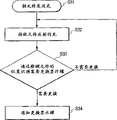
The information collecting device 15 that has driven is like this gathered the environmental information around the device of ink tanks the inside, as ink remaining amount, and ink kind, temperature, (step S11 among Fig. 4) such as pH value and internal pressures.Afterwards, recognition device 16 is read the condition (step S12 Fig. 4) of the internal information contrast of the ink that will obtain with information collecting device from information-storing device 17.Thus, condition of reading and the jar internal information contrast that collects, and whether definite information will transmit (step S13 among Fig. 4).Here, discern according to the predetermined condition of information-storing device 17.Whether to become the pH value that is lower than designated value (for example 2ml), ink by ink remaining amount, whether internal pressure etc. change too big, determine whether to change ink tank.
Among the step S13, recognition device 16 is determined not need the current inner case of ink tank is delivered to the outside, and so, the present case information in the ink tank just accumulation is stored in (step S14 among Fig. 4) on the information-storing device 17.Here, the information of recognition device 16 back that can collect contrast with the information and the information collecting device 15 of this accumulation.
And in the step 13, if recognition device 16 determines that the internal information of ink tank will be delivered to the outside, the electrical power that information transfer device 18 obtains energy conversion device converts to the ink tank internal information is delivered to the energy that usefulness is gone in the outside.Here, can be used as this energy that effectively transmits usefulness and comprise magnetic field, light, shape, color, electric wave, sound etc.Afterwards, find ink remaining amount,, need to change ink tank (step S15 among Fig. 4) with the outside B (for example, ink-jet printer) of sound notification less than specified amount.And, transmit terminal and need not to be ink-jet printer, use up in the practice, shape, color, or during sound, the terminal of transmission also can be people's eyesight or a hearing.And, also can change transfer device, as with the transmission sound device that transmits ink remaining amount, use the light delivery device of transmission ink pH value etc.
When the solid semiconductor device of Gou Chenging is used for ink-jet printer here, can be on the home position of carrying out recovery operation, on the home position that the Inkjet Cartridge of carrying out printing returns, Inkjet Cartridge originally on one's body, or on the printhead, power supply device is installed, and it is to the electromotive force of device supply as external energy; Except that this arrangement,, also can understand the inner case of ink tank without ink-jet printer as long as when the device of the device of supplying with this electromotive force is arranged.So for example, other situation has, effectively check ink tank in factory or workshop available devices, therefore, can sell high-quality ink tank.
Press present embodiment, device is provided with energy conversion device.Therefore, do not need to be provided with and outside direct-connected any electric wire.As a result, this device can be set and be used in any object Anywhere the device of shown in following Figure 13 to 16 that will illustrate, settling in the ink.With the device that is located in the ink, can understand the present case of ink real-time and accurately.
And, with the energy conversion device that offers device, this does not just need to be provided with the storage device (electric power source in the present embodiment) of the electromotive force that the savings operated device uses, therefore, can make device miniaturization, thereby it can be used in any position of object, for example in the very narrow position shown in Figure 13 and 16 or in the ink.Here, in the present embodiment, supply with electromotive force with contact mode not, but also can use the pattern supply electromotive force that temporarily contacts with the outside, subsequently, it becomes with the outside and does not contact.
In this respect, when the FeRAN that makes with ferroelectric material was used as information-storing device 17, it can be as DRAM (dynamic random access memory) high speed read and write data commonly used.And this device becomes the nonvolatile memory that still can remember data when the power supply supply ends.For this reason, FeRAM has higher access probability.Because FeRAM is a nonvolatile memory, unstable even electrical power is supplied with, it can not eliminate data yet, and therefore, solid semiconductor device can be effectively used to ink tank.With the information that the FeRAM storage will accumulate, it is process information exactly, and drives this device under low-voltage, carries out the bidirectional information transmission with external equipment.In this respect, can make the littler semiconductor devices that can under low-voltage, drive with semiconductor technology.As mentioned above, the possible zero access of FeRAM, it is non-volatile simultaneously, so, unstable even electrical power is supplied with, can not eliminate data yet, and, can make power consumption reduce to minimum.Be configured for the extremely effectively information-storing device of solid semiconductor device with the FeRAM that these advantages are arranged.It is effective especially that the solid semiconductor device that these advantages are arranged is used for ink tank, and this is in following meeting explanation.
And, the FeRAM that makes with ferroelectric material makes information-storing device 17, if the ferroelectric material with FeRAM is made capacitor, can make the capacitance of solid semiconductor device bigger, the bigger capacitance of set solid semiconductor device, when solid semiconductor device and external equipment carry out signal when transmitting, the transmission frequency of solid semiconductor device is reduced, this will illustrate afterwards.As a result, the frequency that solid semiconductor device can be lower is carried out the information transmission, transmits the free degree to improve.
The 2nd embodiment
Fig. 5 is the block diagram of explanation by the internal structure of the solid semiconductor device of the present invention the 2nd embodiment, and, also show it and outside transmission situation, the solid semiconductor device of present embodiment shown in Figure 5 comprises: energy conversion device 24 converts electrical power 23 with the not way of contact from the electromotive force 22 that outside A supplies with device 21 with its handle; Information collecting device 25, it is driven by the electrical power that energy conversion device 24 obtains; Recognition device 26; Information transfer device 27; Information-storing device 28; With receiving system 29.These devices are arranged in the ink tank.With the difference of the 1st embodiment is that it has the function of received signal.And can use electromagnetic induction, and heat, light, ray is as the required electromotive force of operated device.And, preferably from the teeth outwards or near surface form energy conversion device 24 at least, information collecting device 25 and receiving system 29.In this respect, as mentioned above, the FeRAM configuration information storage device 27 made of the most handy ferroelectric material also.
Information collecting device 25 is gathered the environment around the device 21 in the ink tank.Information receiver 29 is received from the signal 20 of outside A or outside B input.Recognition device 26 can make information collecting device 25 by the information of gathering ink tank inside from the input signal of receiving system 29, and, whether satisfy the condition of appointment with the information of the jar inside determining to collect the inner information contrast of the jar that is stored in information and collection on the information-storing device 27.Information-storing device 27 storages will be made the various conditions of contrast and the jar internal information that is collected by information collecting device 25 with the information of the jar inside of gathering.Information transfer device 28 converts electrical power to the transmission jar required energy of internal information according to the instruction of self-identifying device 26, and afterwards, externally A shows the recognition result that recognition device 26 provides on outside B or the outside C, and the result is transmitted accordingly.
Fig. 6 is the operational flowchart of explanation device shown in Figure 5.Among Fig. 5 and Fig. 6, by outside A electromotive force 22 is supplied with device 21, afterwards, power conversion is put 24 electromotive force 22 and is converted electrical power 23 to.Electrical power excitation information harvester 25, recognition device 26, information-storing device 27, information transfer device 28 and receiving system 29 with such conversion.
Under this condition, the signal 30 that is used to inquire about the ink tank internal information sends to device 21 with outside A or B.It is this input signal 30 (Fig. 6 step S21) that is used for for example inquiring about the signal that whether also leaves ink in the ink tank that receiving system 29 receives.Afterwards, the information that recognition device 26 can make information collecting device 25 gather in the ink is as residual ink amount, the kind of ink, temperature and pH value (step S22 among Fig. 6), and, condition (step S23 Fig. 6) read from information-storing device 27 as the jar internal information benchmark that collects.Determine thus whether the information that is collected satisfies the condition (step S24 among Fig. 6) that sets.
Can not satisfy the condition that sets if in step S24, send the information that is collected, then unappeasable information be passed to outside A, among B or the C.If the condition that the information conforms that discovery collects is set is then correspondingly transmitted information (step S25 and S26).At this moment, can be delivered to the outside with recognition result with the information that collects.Convert this transmission operation of information transfer device 28 execution that the information of ink tank the inside is delivered to outside institute energy requirement to the electrical power that energy conversion device is obtained.Available magnetic field, light, shape, color, electric wave, sound etc. are as carrying out the energy that this transmits usefulness, and transfer mode can be by the recognition result conversion, also can be the content conversion transfer mode of the problem that will answer, for example, whether (for example, 2ml) to press ink remaining amount less than specified amount, perhaps, whether the pH value of ink changes and waits the conversion transfer mode.
And, also can be electromotive force with supplying with device 21 from the signal 30 of outside A or B input.For example, when being electromagnetic induction as if energy, electromotive force can be used as the signal of inquiring about ink remaining amount; If energy is a light, electromotive force can be used as the signal of the pH value of inquiring about ink.
Press present embodiment, the function that receives external signal is provided.Therefore, except that obtaining the effect from the 1st embodiment, present embodiment also has the function of answering from the problem of the various signallings of outside, so its can performer and outside bi-directional.
In this respect, the preferred device that is arranged in the ink tank has been described, therefore, has supposed that device is provided with information collecting device.But, understand that the basic structure of present embodiment is the solid semiconductor device that does not have information collecting device, still, can respond from the signal of outside input the information on the device of storage is in advance outputed to the outside.
The 3rd embodiment
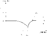
Fig. 7 is the block diagram of displaying by the internal structure of the solid semiconductor device of the present invention the 3rd embodiment, and shows it and outside transmission situation.Solid semiconductor device 31 by present embodiment shown in Figure 7 comprises: energy conversion device 34, and it converts the electromotive force 32 of supplying with device 31 with the not way of contact from outside A to electrical power 33; Buoyancy generating means 35, it produces buoyancy with the electrical power that energy conversion device 34 obtains.These devices are arranged in the ink tank.
Press present embodiment, when outside A supplied with electromotive force 32 for device 31, energy conversion device 34 converted electromotive force 32 to electrical power 33.Buoyancy generating means 35 electric powers 33 produce buoyancy, and device 31 can be floated on the ink level.Device is stayed on the ink level this buoyancy needn't be set, still, ink release occurs in order to prevent the state that no longer includes ink, device can be positioned at the distance of regulation under the liquid level in any case.
For example, Fig. 8 A and 8B demonstrate the position of staying the device 31 in the ink in the ink tank with the variation of consumption of ink.In the ink tank that constitutes with the absorption chamber of the chamber of direct dress ink and interior dress negative pressure generation part, transmit with transmitting portions 39, shown in Fig. 8 A, stay quantity of ink in the negative pressure generation part 37 and equal the used up quantity of ink of drawing through ink guide part 36 from negative pressure generation part 37.Therefore, solid semiconductor device 31 moves along the position that ink level H is descended in the ink 38, and still stays distance specific under the ink level H, shown in Fig. 8 B.
Fig. 9 is the flow chart that confirms the position of device 31, and determines whether need to change ink tank referring to the step S31 to S34 among Fig. 7 and Fig. 9, launches light from outside A or (for example, ink-jet printer) to device 31.Afterwards, outside A, B (for example, ink-jet printer) or C receive light, the position of detection means 31 thus.Afterwards, ink-jet printer determines whether needs replacing ink tank according to detected device position.If finding needs to change ink tank, then make corresponding notice with sound or light.
With regard to this detection of device position, when not allowing light to pass device, be oppositely arranged light-emitting device and light-sensitive unit, to confirm the position of device, perhaps,, also can confirm the position of device when light-sensitive unit detected from the reflection of light light time of light-emitting device emission.And, to illustrate that as following can be provided with solid semiconductor device 31 itself become light-emitting device, and to being located at jar outside luminous structure of light-sensitive unit.
Press present embodiment, even because the liquid specific gravity in the place of use device or the difference of other environmental aspect, when the buoyancy of device or other similar requirement can change, by the electromotive force that comes conversion to supply with energy conversion device by the outside, can make device always be positioned at desired position, therefore, the environment around the tube device and use device not.
At this on the one hand, present embodiment can be in conjunction with the 1st above-mentioned embodiment and the 2nd embodiment.
The 4th embodiment
Figure 10 A to 10C is the concept map of explanation by the using method of the solid semiconductor device of the present invention the 4th embodiment.
Solid semiconductor device by the 1st or the 2nd embodiment is added that the information transfer function that communicates information on a plurality of other devices also is arranged on a plurality of this devices in the object, constitutes present embodiment.
In Figure 10 A institute example, be provided with a plurality of solid semiconductors in the object by the 1st embodiment.When outside A or B supply with each device electromotive force E, each device in these devices is inquired about the environmental information around the device respectively.Afterwards, the Information Monitoring a of device 41 is delivered to device 42.Afterwards, the information a and the b that collect of device 41 and 42 is delivered to next device in succession.Last device 43 is delivered to outside A or B to the information that all collects.
And, in the example shown in Figure 10 B, a plurality of solid semiconductor devices by the 2nd embodiment are set in the object, supply with each device electromotive force E by outside A or B.Afterwards, when the problem Q after the concrete signalization when outside A or B are input into device 53, for example, respond the content of this problem, device 51 or 52 is gathered the information of correspondence problems and is also answered this problem.The answer that device 51 or 52 draws this problem is delivered to other device in succession, draws answer by the device 53 that requires and is delivered to outside A, B or C.
In Figure 10 C institute example, a plurality of solid semiconductor devices by the 2nd embodiment are set in the object, supply with each device electromotive force E by outside A or B.Afterwards, when certain signal was input to device 63 by outside A or B, this signal was delivered to device 62 and 61 in succession, and is presented at outside A from device 63, on B or the C.
Here, in Figure 10 A to 10C example, the solid semiconductor device by the 3rd embodiment that is provided with the buoyancy generating means can be used as one of a plurality of solid semiconductor devices.
Be provided with respectively the solid semiconductor device that forms through appropriate combination by the the 1st, the 2 or the 3rd those devices of implementing in ink tank and printhead in the structure example shown in Figure 11.Among Figure 11, reference symbol W marks the direction of printing (printing) scanning and the direction that E marks electromotive force.In this example, solid semiconductor device 71 adds on the 1st embodiment device and has the buoyancy generating means, and having the 3rd embodiment that transmits the information transfer function of information to other device 79 to constitute, solid semiconductor device 71 is located at the assigned address in the ink 73 in the ink tank 72.On the other hand, printhead 78 discharges fluid path 75 and the liquid chamber ink supplied that is connected with the providing ink part 74 of black flow container 72 by blowing part 77, and printhead also is provided with ID function (recognition function) and is added to the solid semiconductor device 79 that constitutes by the solid semiconductor device of the 2nd embodiment.The electrode part that is located on the device surface is contacted with the lip-deep contact portion that is located at the electric base plate that drives printhead 78, supply with electrical power for device 79.
Afterwards, supply with electromotive force for from the outside each device 71 and 79, the device 71 in the ink is gathered the ink remaining amount signal, and for example, the device of printing on the first side 79 determines to change the required id information of ink tank for device 71 transmission.Then, ink remaining amount information and id information that device 71 relatively obtains, if consistent between them, the outside ink tank of changing of the indication of just communicating by letter with device 79.When receiving the instruction of such transmission, device 79 is given the outside signal of changing ink tank that sends, and corresponding sound or light are exported in the perhaps attracting eyesight or the sense of hearing.
As mentioned above, a plurality of devices are arranged in the object, just can determine complicated information status.
The structure of Figure 10 A to 10C and example shown in Figure 11 is give each solid semiconductor device power supply kinetic potential, but the structure setting to be not limited thereto.Electromotive force and the desired information of also can bar structure being arranged to supply with certain device send to another device together in succession.For example, shown in Figure 12, give the buoyancy generating means that adds the 3rd embodiment by the solid semiconductor device of the 1st embodiment, the function of transmitting information for other device, and the function of supplying with electromotive force constitute solid semiconductor device 81; Give the buoyancy generating means that adds the 3rd embodiment by the solid semiconductor device of the 2nd embodiment, the function of transmitting information for other device, and the function of supplying with electromotive force constitute solid semiconductor device 82; Respectively solid semiconductor device 81 and 82 is arranged in the ink 73 in the ink tank 72 by method shown in Figure 11.On the other hand, printhead 78 is connected with ink tank 72, and printhead 78 is provided with the solid semiconductor device 83 by the 2nd embodiment of band ID function (recognition function).Make electrode part on the device surface contact to device 83 and supply with electrical power with contact portion on being located at the electric base plate that drives printhead 78.Among Figure 12, reference symbol E indicates electromotive force, W indication printing scanning direction.
When supplying with electrical power for device 81 from the outside, the device of staying in the ink 81 is gathered ink remaining amount information, for example, the interior condition of this information and regulation is contrasted, if find and to exchange with other device, then the information of the ink remaining amount that collects and electromotive force are passed to device 82 together and come operated device 82.The device 82 of having received the electromotive force of supply receives the information of transmitting the ink remaining amount that comes from device 81, simultaneously, gathers the information of ink pH value, and for example, afterwards, electromotive force sends to the device of printing on the first side 83, with operated device 83.The device 83 printing on the first side that receives the electromotive force of supplying with like this is delivered to device 82 to id information, to determine to change required ink remaining amount or the current pH value of definite ink of ink tank.Afterwards, device 82 is the contrast of the id information of the signal of the ink remaining amount that collects and pH value signal and transmission, if their unanimity, the instruction of communicating by letter and transmitting the replacing ink tank to outside with device 83.Receive this instruction, device 83 is given the outside signal of changing ink tank that sends, or exports corresponding sound or light for people's the vision or the sense of hearing.In this way, can imagine and supply with the method that electromotive force is supplied with information needed simultaneously for other device by certain device.
In this respect, printhead 78 can be used known blowing pattern in the inkjet printing field, wherein, with the heat that the heater of for example electricity-heat converter produces, the ink in the heating liquid flow passage, make the ink foaming, thus, make ink from each thin opening that each liquid communication path is communicated with emit, perhaps, adopt the structure that discharges ink with the driving piezo-electric device.
Figure 13 to 16 is the structure charts with the ink tank of the solid semiconductor device of the foregoing description.Ink tank 501 shown in Figure 13 has the soft China ink bag 502 that is arranged on interior dress ink in the shell 503, and black bagmouths open 502a seals with the rubber stopper 504 that is fixed on the shell 503.When the saturating rubber stopper 504 of hollow needle 505 thorns that are used to draw ink, ink is added to ink jet-print head (not having picture).Can be by this method being arranged in the China ink bag 502 of this ink tank 501 by solid semiconductor device 506 of the present invention.
And, ink tank 511 shown in Figure 14 have the shell 512 that is located at dress ink 513 ink guide part 514 with the ink jet-print head 515 on printing paper S, printed of release ink.It is possible solid semiconductor device 516 of the present invention being located in the ink 513 of ink tank 511.
And, the porous member 532 that keeps ink is housed in the ink tank 531 shown in Figure 16.So, the ink printed that dress ink jet-print head 533 usefulness thereon keep like this.The ink tank 531 that constitutes by this mode.Solid semiconductor device 534 and 535 be separately positioned in ink tank one side and the first side of inkjet printing in.Its advantage is that the ink in each member spaced apart from each other can circulate mutually.
Figure 17 is equipped with the structural representation of setting by the ink-jet printer of the ink tank of solid semiconductor device of the present invention on it.The printhead Inkjet Cartridge of installing on the ink jet recording device 600 shown in Figure 17 601 comprises: the release head that discharges the liquid of the ink that is used to print; With the ink tank shown in Figure 13 to 16, to keep the liquid of wanting feed fluid to discharge head.And, in the recording equipment 600, be provided with to being located at solid semiconductor device in the ink tank and supply with power supply device 622 and information transfer device (not shown) as the electromotive force of external energy, be used for carrying out the information bidirectional transmission with these devices.
As shown in figure 17, printhead Inkjet Cartridge 601 is installed on the travelling carriage 607, thread groove 606 engagements of travelling carriage 607 and screw mandrel 605, screw mandrel 605 through driving power transmission gear 603 and 604 with CD-ROM drive motor 602 rotate and reverse and the rotation of interlocking.With CD-ROM drive motor 602 drivings printhead Inkjet Cartridge 601 and travelling carriage 607 are moved back and forth together along the direction of guide rod 608 by arrow a and b indication.Ink jet recording device 600 is provided with recording medium loading attachment (not having picture), be used for the printing paper P of recording medium that device can be used as the liquid of the black liquid that receives as discharge from Inkjet Cartridge 601, if pressing plate 610 is pressed on the platen 609 on the moving direction of travelling carriage 607 be contained in printing paper P on the platen 609 with the recording medium loading attachment with its.
Near screw mandrel 605 1 ends, photo-coupler 611 and 612 are set.Photo-coupler 611 and 612 constitutes the in situ detection devices, with the control lever 607a of its identification travelling carriage 607 whether in photo-coupler 611 and 612 zones that constitute, to switch the rotation direction of CD-ROM drive motor 602.Near one end of platen 609, supporting member 613 is set, covers the lid 614 of the blowing front end partly of printhead Inkjet Cartridge 601 with supporting.Also be provided with blotter 615, remain in the ink in the lid 614 when not putting ink because of printhead Inkjet Cartridge 601 with its sucking-off.Make printhead Inkjet Cartridge 601 can recover the blotting function with this blotter 615 through the opening of lid 614.
Ink jet recording device 600 is provided with body abutment part 619, makes this body abutment part 619 by advancing and Return-ing direction, promptly perpendicular to the direction of the moving direction of travelling carriage 607, supports displaceable member 618 movably.On the displaceable member 618, cleaning foil 617 is housed.The pattern of cleaning foil 617 is not limited thereto.The cleaning foil of any existing pattern can both be used.And, when carrying out the blotting recovery operation, the control lever 620 as the beginning blotting is set with blotter 615.Control lever 620 is along with moving with the moving of cam 621 of travelling carriage 607 engagement, and detects moving of it with known transfer mode, for example cuts off the driving electrical power of electric drive motor 602 supplies and controls the mobile of it.On printer main body one side, ink jet printing controller is set, it sends to signal and is used for the set heater element of printhead Inkjet Cartridge 601, and each above-mentioned mechanism is driven control.Do not have picture among this controller Figure 17.
The ink jet recording device 600 of Gou Chenging can make printhead Inkjet Cartridge 601 move back and forth on the whole width of printing paper like this.Loading attachment with above-mentioned loaded recording medium is loaded in printing paper P on the platen 609.When driving signal supply device (not having picture) driving signal supply printhead Inkjet Cartridge 601 when the printhead Inkjet Cartridge moves, black liquid (record liquid) is discharged into from the liquid delivery head unit on the recording medium so that print by these signals.
The 5th embodiment
Figure 18 is the block diagram of displaying by the internal structure of the solid semiconductor device of the present invention the 5th embodiment.It and external communications.Solid semiconductor device 91 shown in Figure 180 comprises; Energy conversion device 94, it is converting electrical power 93 to from the outside by the electromotive force 92 as external energy of not way of contact supply device 91; With light-emitting device 95, it uses the electrical power that is obtained by energy conversion device 94 luminous.Device is arranged in the ink in the ink tank.With formation light-emitting devices 95 such as photodiodes.
In this respect, electromagnetic induction, heat, light, ray etc. can be used as the electromotive force that operated device is supplied with.And, require near device surface or device surface, to constitute energy conversion device 94 and light-emitting device 95.
In the present embodiment, when outside A supplied with electromotive force 92 for device 91, energy conversion device 94 converted electromotive force 92 to electrical power 93.Afterwards, light-emitting device 95 electric powers 93 luminous 96.Detect from the light intensity of light-emitting device 95 emissions with outside B.
Figure 19 is the structural representation of having used by the ink tank of the solid semiconductor device of the 5th embodiment.Solid semiconductor device 91 shown in Figure 19 floats near the liquid level of original ink 522 of ink tank 521, is located at the electromagnetic induction that the external resonant circuit (not having picture) of ink tank 521 outsides supplies with and induces electromotive force.So the photodiode that drives the near surface that is located at solid semiconductor device 91 is luminous.The optical sensor 97 of ink tank 521 outsides receives the light that sees through ink 522.
Figure 20 is the wavelength attenuation curve map (absorption spectra) of exemplary ink (yellow (Y), dark red (M), blue green (C) and black (B)).From curve shown in Figure 20 as can be seen, yellow, peony, blue green and black ink separately the peak Distribution of the attenuation rate of wavelength in 300 to 700nm wavelength period.The wavelength attenuation rate peak value of yellow ink is about 390nm, and wine-colored wavelength attenuation rate peak value is about 500nm, and the wavelength attenuation rate peak value of black is about 590nm, and blue green wavelength attenuation rate peak value is about 620nm.Therefore, at 300 to 700nm light, afterwards, receive this light that sees through ink, from the solid semiconductor device emission wavelength ranges to detect maximum absorbing wavelength with the optical sensor (seeing Figure 19) that is located at the ink tank outside.Can discern the color of ink with the light that sees through above-mentioned ink color by this mode.
Can see that from Figure 20 yellow, peony, blue green and black ink are different fully in the wavelength attenuation rate of 500nm.Attenuation rate at the ink of every kind of color of 500nm wavelength is that peony is about 80%, and black is about 50%, and yellow is about 20%, and blue green is about 5%.Therefore, detect the color that just can identify the ink that permission light sees through about the luminous intensity that sees through ink of 500nm wavelength and ratio (transmissivity) from the ink of above-mentioned those colors by the luminous intensity of solid semiconductor device emission.
Here, in any case above-mentioned, a kind of solid semiconductor device is set respectively in different ink tanks just can discerns multiple color.
And, ink-jet printer is constituted, in a plurality of ink tanks each is put on each assigned address according to the ink kind of adorning in them, if warning device, when the optical sensor 97 with the light that receive to see through the ink in the ink tank detects ink tank and correctly is not placed on the assigned address, the user is given the alarm.Warning device in this case can be with the light-emitting device as lamp, as the sound-producing device of buzzer.The alarm of sending with these devices makes the user know that ink tank is placed on inappropriate position, correctly is installed in ink tank on the assigned address so again.
Perhaps, control device is set for this ink-jet printer, when being installed on the unsuitable position to ink tank, can control printhead according to the ink kind that will be added on this printhead from dress ink tank thereon with the light sensors that receives the light that sees through the ink in the ink tank.Use this control, even also can automatically carry out recovery operation when the user is placed on the unsuitable position to ink tank, therefore, and as long as replenish ink in the printhead, print image suitably just.And the user is no longer too responsive to the installation position of ink tank.
As mentioned above, by the present invention, be provided with energy conversion device, with it external energy converted to different types of energy, light-emitting device is luminous with the such energy after conversion of energy conversion device.Therefore, by the intensity of the transmission light wavelength behind the light transmission ink that detects the solid semiconductor device emission, just can discern the kind of ink.
Solid semiconductor device by the 5th embodiment is provided with light-emitting device, except know the ink kind in other ink tank in ink tank with it, also following use can be arranged.
For example, with the structure of this device, can test the variation of the fluid continuous-flow of Reynolds (Reynolds) liquid.In other words, the solid semiconductor device that is provided with light-emitting device is imbedded on the side of the pipe that liquid flow is wherein arranged, and device is exposed in the pipe, afterwards, light-sensitive device (this device also can constitute with solid semiconductor device itself) is set on its opposite face.Here, for example, when gasoline that is used for car engine and air mixing, but regulator solution stream, perhaps, but the blockage of tracer liquid pipeline such as city water pipe.
Also have, for example, when the running status by model configuration obtained desired data, device was useful.In this case, for example, the assigned address that requires at element correctly is provided with the solid semiconductor device of the light-emitting device of specified wavelength, so that carry out concrete operation, afterwards, drives this structure and operates, and the running status by detection means obtains data.Here, available solid semiconductor device obtains the result with the function of carrying out appointment with the discontiguous mode in outside.More particularly, can detect the running status of driving element, this driving element operation is emitted the ink that is contained in the ink jet-print head.For example, the correct setting of each actuator has the device that wavelength is respectively the light-emitting device of 300nm, 400nm, 500nm and 600nm, afterwards, detect light, can test the moving of each actuator of the running state information that is used to gather each actuator from blowing part one side.
The 6th embodiment
Figure 21 is the cross-sectional schematic of ink tank, and this ink tank can be used the solid semiconductor device by the present invention the 6th embodiment.Figure 22 is the block diagram of showing the internal structure of solid semiconductor device shown in Figure 21, and shows it and outside transmission situation.
As shown in figure 21, ink tank 101 comprises the chamber 102 and the ink guide part 103 of device ink, and the ink that is contained in the black chamber 102 is supplied with ink jet-print head 104 through ink guide part 103.Printhead 104 is detachably connected to ink tank 101 or is fixedly attached to ink guide part 103.Emit from a plurality of China inks mouthful (not having picture) of putting by ink tank 101 ink supplied according to print signal, on recording medium, print.The ink of being supplied with printhead 104 by ink tank 101 makes ink stay each with capillarity and capillary balance and puts in (China ink) material mouth.In order to prevent in the operation that ink spills when not printing from printhead 104, the inside of adorning black chamber 102 keeps negative pressure.
With regard to ink tank 101, solid semiconductor device (being designated hereinafter simply as " device ") 111 fixed by the state that its part is exposed at ink tank 101 outsides, and another part of device is exposed at the inside of adorning black chamber 102.Although the fixed position of device 111 needn't be limited, but, ink tank 101 in use, at least be exposed at the device portions of adorning in the black chamber 102 should be placed on can not with the ink position contacting, perhaps, when using ink tank, be exposed at the device portions of adorning in the black chamber 102 and preferably be placed on the upper wall portion of ink tank 101.
The functional structure of device 111 is described referring to Figure 22 now.
Among Figure 22, device 111 comprises: energy conversion device 114, and it converts the electromotive force 112 that the outside A from ink tank 101 supplies with device 111 by the not way of contact to electrical power 113; Pressure-detecting device 115, the electrical power 113 after it is changed with energy conversion device 114 drives; Recognition device 116; Information storage (accumulation) device 117; With regulator 118.The operated device 111 and electromotive force supplied with can be used electromagnetic induction, heat, light, ray etc.And, on the surface of device 111 or near surface to form energy conversion device 114 at least.In this respect, preferably use above-mentioned FeRAM configuration information accumulation device 117.
Pressure-detecting device 115 detects the internal pressure as the ink tank of device 111 environmental information on every side, and this information is outputed to recognition device 116.The available pressure sensor is made pressure-detecting device 115, and it has the device of being positioned at 111 lip-deep diaphragms, and for example, the displacement that changes the film that produces according to pressure comes detected pressures.
Figure 23 is the operational flowchart of explanation device shown in Figure 22.Now, referring to Figure 21 to 23, when the outside A from ink tank 101 supplied with electromotive force 112 for device 111, energy conversion device 114 converted electromotive force 112 to electrical power 113.Electronic rate 113 activation pressure checkout gears 115, recognition device 116, information transfer device 117 and regulator 118 with such supply.
Driven pressure-detecting device 115 detects the internal pressure (step S111 among Figure 23) of ink tank 101.Afterwards, recognition device 116 is read from the information (step S wants 112 Figure 23) of information-storing device 117 accumulation, and the internal pressure information contrast of condition of reading like this and detected jar, the internal pressure (step S113 among Figure 23) that determines whether to need to regulate ink tank 101 thus.In this respect, when the ink of filling from factory will transport, set initial pressure (step S116 among Figure 23) in the ink tank 101 with special inspecting equipment, and this information is gone up (step S117 among Figure 23) as the ROM that the raw information of this batch product (scope of application of appointment (R) among Figure 36) writes on device 111.Among Figure 36, reference symbol S is meant the halted state of printing, and VO and VC refer to the Kai Heguan of valve respectively.
Among the step S113, if the internal pressure of detected ink tank 101 is in the internal pressure scope of information-storing device 117 accumulation, so, recognition device 116 definite internal pressures that do not need to regulate ink tank 101, do not drive regulator 118, and ink tank 101 current internal informations are accumulated in (step S114 among Figure 23) on the information-storing device 117.Here, Figure 36 illustrates the example of storage internal pressure.In this way, can understand the transient change of negative pressure with the consumption of ink in the ink tank 101, and the transient change of negative pressure in the continuous sweep process of printhead.This information sends to the control circuit of printhead, makes the recovery operation performance best and set the drive condition of printhead.
And, in step S113, if the negative pressure of detected ink tank 101 is lower than the higher limit that the interior pressure of the ink tank 101 that is stored on the information-storing device 117 is provided with, the recognition device 116 definite internal pressures that will regulate ink tank 101 drive regulators 118 with the electrical power 113 after energy conversion device 115 conversions.Here, if regulator 118 is valve mechanisms, (step S115 among Figure 23) regulates the internal pressure of ink tank 101 then as stated above.
When device 111 was used for ink-jet printer, the optimum position of supplying with as the device of the electromotive force of external energy was the position of printhead and travelling carriage, the recovery position of printhead, or the answer position of printhead, or the like be used for various types of ink-jet printers.In addition, if use the device that is provided with the electromotive force feedway, also can understand the internal state of ink tank even without ink-jet printer.Therefore, practically ink tank is not installed to the internal pressure that yet can regulate ink tank on the ink-jet printer in factory or workshop.
As mentioned above, with the device 111 that is located in the ink tank 101, also can detect the internal pressure of ink tank 101 and it is adjusted to the pressure of regulation if supply with electromotive force 112 only for device 111.As a result, to make the inside of ink tank 101 remain on the quantity of ink of no matter staying in the ink tank 101 be what also can make under the best condition of negative pressure that ink emits from printhead 104.Therefore, stably supply with ink can for printhead 104.Thereby do not need ink to be stayed in the ink tank to keep the condition of negative pressure of ink tank 101 inside as absorbing ink with the blotting material in the prior art.Thereby, can improve the black efficient of storage.
And, by the present invention,, just no longer need to establish any and outside direct-connected electric wire because device 111 is provided with energy conversion device 115, therefore, even all can use device 111 in any position that can not be connected with the outside.And with the device 111 that is provided with energy conversion device 115, device 111 is not provided with the storage device (for example, in this example being electric power source) of the electromotive force of storing driver device 111.Therefore, can do device 111 forr a short time, and can use device 111 in any position in object.In other words, device 111 can be arranged on the optimum position in the ink tank 101.Here, with regard to present embodiment, supply with electromotive force for device 111, still, also can use with the of short duration mode that contacts in outside and supply with electromotive force, afterwards, make it again and do not contact outward to device by the not way of contact.
The 7th embodiment
Figure 24 is the block diagram of internal structure of the solid semiconductor device of explanation the 7th embodiment, and it and outside transmission situation are shown.Solid semiconductor device shown in Figure 24 (hereinafter to be referred as " device ") 121 is fixed to ink tank (not having picture) by the mode identical with device shown in Figure 21 111.Device 121 comprises: energy conversion device 124, and it converts the electromotive force 122 that the outside A of ink tank supplies with device 121 by the not way of contact to electrical power 123; Pressure-detecting device 125; Recognition device 126; Information storage (accumulation) device 127; Regulator 128; With receiving system 129, these devices are all with the electrical power excitation after energy conversion device 124 conversions.The difference of present embodiment and the 6th embodiment is, it has the function of received signal, that is, it has receiving system 129.Available electromagnetic induction, the electromotive force 122 that heat, light and ray etc. are supplied with as exciter component 121.And, at the surface or the near surface of device 121 energy conversion device 124 and receiving system 129 are set at least.
The internal pressure of the ink tank of pressure-detecting device 125 detection means 121 ambient condition information, and this information outputed to recognition device 126.Receiving system 129 receives the outside A of the supply source of electromotive force 122 naturally or from the input signal 130 of the outside B different with outside A.Recognition device 126 can make the internal pressure of pressure-detecting device 125 bases from the input signal detection ink tank of receiving system 129, and, determine thus whether the internal pressure information of detected ink tank satisfies the condition that makes the printhead (not having picture) that is contained on the ink tank discharge ink the internal information of detected like this ink tank and the information contrast that is stored on the information-storing device 127.The information of information-storing device 127 these conditions of storage and the ink itself that obtains by pressure-detecting device 125.Drive regulator 128 with energy conversion device 124 electrical power supplied, regulate the internal pressure of ink tank with the instruction of sending by recognition device 126.Can be by the described method working pressure of the 6th embodiment checkout gear 125 and regulator 128.
Figure 25 is the flow chart of the operation of explanation device shown in Figure 24.Referring to Figure 24 and Figure 25, when when outside A supplies with device 121 electromotive force 122, energy conversion device 124 converts electromotive force 122 to electrical power 123, electric power activation pressure checkout gear 125, recognition device 126, information-storing device 127, regulator 128 and receiving system 129.
Under this state, receiving system 129 receives the input signal 130 (step S121 Figure 25) that sends to device 121 from outside A or B.The internal pressure of 130 pairs of devices of this input signal, 121 inquiry ink tanks.This input signal 130 can be supplied with device 121 with electromotive force 122.
When receiving input signal 130, recognition device 126 makes pressure-detecting device 125 detect the internal pressure (step S122 among Figure 25) of ink tank, and read canned data (step S123 Figure 25) from information-storing device 127, determine thus whether detected internal pressure information satisfies above-mentioned condition (step S124 among Figure 25).In this respect, set initial pressure (step S126 among Figure 25) in the ink tank with special-purpose checkout facility when in factory, filling ink and will transport, and the ROM that the information of this batch product writes on device 121 is gone up (scope of application of pointing out among Figure 37 (R)) as initial information (Figure 25 step S127).
Among the step S124,, then drive the internal pressure (step S125 among Figure 25) that regulator 128 is regulated ink tank if find that detected internal pressure can not satisfy condition.On the other hand, if detected internal pressure satisfies condition, then the current internal pressure information of ink tank is stored in (step S128 among Figure 25) on the information-storing device 127.In this respect, Figure 37 illustrates the example of the stored information of internal pressure.Among Figure 37, reference symbol VO and VC indicate the opening and closing of valve respectively, and S indication printing suspends.In this way, can understand the transient change of negative pressure with the consumption of ink in the ink tank, and in printhead continuous sweep process the transient change of negative pressure.The control circuit that this information sends to printhead can make the recovery operation performance reach best and set the drive condition of printhead.
Press present embodiment, the function of the signal that reception comes from the outside is arranged, except the effect that the 6th embodiment is obtained, it can also respond the problem from the various signallings of outside, and between device and outside bi-directional information.
Here with a device 121 that is provided with pressure-detecting device 125 and regulator 128 present embodiment has been described.But, pressure-detecting device and regulator are set also can for each different devices separately.Afterwards, bar structure is arranged to detect the internal pressure of ink tank to determine whether to need to regulate the internal pressure of ink tank with a device, if find to need regulate its internal pressure, just notice is provided with the internal pressure that another device of regulator is regulated ink tank.
Now the concrete structure example of regulator and its manufacturing step are explained together.
Figure 26 is provided in a side of the structure example schematic diagram by the regulator on the solid semiconductor device of the present invention, and shows device and be formed on the situation on the spherical silicon of described semiconductor spheres.Figure 27 A to 27G is the schematic diagram of the manufacturing process of explanation regulator shown in Figure 26.In this respect, Figure 26 and Figure 27 A to 27G are the cutaway views of cutting open from the center of spherical silicon.
As shown in figure 26, form a base stage 201 respectively in two positions respect to one another of spherical silicon 200.And, around spherical silicon 200, form SiN film 206.SiN film 206 forms the cantilevered moveable part 210 and 211 on the area that is bearing in each base stage 201 respect to one another that the surface with spherical silicon 200 separates.Each displaceable member 210 and 211 is respectively equipped with the valve electrode 205 in the face of base stage 201.And SiN film 206 has the gap that separates with spherical silicon 200 parts respectively each area from a base stage 201 to another base stage 201.Each part in these parts all becomes can make the passage 212 that is filled with air between variable moving part 210 1 sides and another displaceable member 211 1 sides.
The manufacture method of regulator shown in Figure 26 is described referring to Figure 27 A to 27G now.
At first, on the whole surface of the spherical silicon 201 shown in Figure 27 A, form PSG (phosphosilicate glass) film 202 shown in Figure 27 B.Here, form before the psg film 202, on spherical silicon 202, be pre-formed each base stage 201 with its centrosymmetric two positions.Afterwards, shown in Figure 27 C, give psg film 202 compositions,, base stage 201 is exposed, and the meeting that will illustrate after making becomes the part of passage and intactly stays so that on psg film 202, form opening 203 with photoetching process.
Afterwards, as Figure 27 1) shown in, form copper (Cu) film 204 that covers base stage 201 and psg film 202 with metal CVD method.Copper film 204 makes base stage 201 and the complete reservation of peripheral part, and other remove.Then, shown in Figure 27 E, on the part that will become the moveable part that the back will illustrate of copper film 204, form valve electrode 205.And, on the entire circumference of spherical silicon 200, form covering psg film 202, the SiN film 206 of Cu film 204 and valve electrode 205 with the PECVD method.
Shown in Figure 27 F,, form the displaceable member shape to SiN film 206 compositions.Figure 28 is the device plane schematic diagram in this step.As shown in figure 28, to SiN film 206 compositions, on the Cu of SiN film 206 membrane portions 204, form radial slot 206a.Afterwards, remove Cu film 204 and psg film 202 with the appropriate solvent dissolving.By this mode, shown in Figure 27 G, obtain with the moveable part 210 and 211 solid semiconductor devices that constitute that lay respectively on the both sides, upper and lower, the function of the valve of the gap supporting that its useful and spherical silicon 200 separates, so the gap between gap between top displaceable member 210 and the spherical silicon 200 and bottom displaceable member 211 and the spherical silicon 200 interconnects with passage 212.
When this solid semiconductor device was installed on the ink tank, a displaceable member 210 was positioned at the outside of ink tank, and another displaceable member 211 is positioned at the inside of ink tank.
Now, referring to Figure 26, Figure 29 and Figure 30 illustrate the pressure regulating method in the ink tank that the solid semiconductor device with regulator is set.
Figure 29 is the equivalent circuit diagram of the electric structure of regulator shown in Figure 26.From Figure 29, see, constitute capacitor C between valve electrode VE respect to one another and the base stage BE.Figure 30 is that signal is added to the valve electrode of regulator shown in Figure 26 and the sequential chart on the base stage.In this respect, reference symbol C indicates the pass, and 0 indication is opened.
At first, base stage 201 and valve electrode 205 are made as the GND level, afterwards, add high level signal for base stage 201, add high level signal also for valve electrode 205.Therefore, electrostatic attraction occurs between valve electrode 205 and the base stage 201, and valve electrode 205 is pushed to base stage 201.As a result, displaceable member 210 and 211 is shifted to spherical silicon 2,000 one sides and is contacted with spherical silicon 200, thus, and the two ends of closing passage 212.Commutation is talked about, and the outside of ink tank and the inside enter not circulation status.
This state is defined as original state, and consumes the ink in the ink tank.Afterwards, use pressure-detecting device (not having picture) to detect the internal pressure of ink tank on request.Negative pressure raises along with the consumption of ink tank ink inside, becomes the negative pressure that is higher than regulation if detect negative pressure, adds low level signal then for valve electrode 205.Thus, make moveable part 210 and 211 separable spherical silicon 200 that passage 212 is unclamped.As a result, air enters ink tank the inside through passage 212 from the outside, and the negative pressure in the ink tank is reduced.Afterwards, when the negative pressure in the ink becomes designated value, add high level signal for again valve electrode 205, make moveable part 210 and 211 move closing passage 212.
By detect poor between the result with pressure-detecting device, or repeatedly repeat to unclamp passage 212 by specific period, or by the testing result that detects the internal pressure of ink tank with pressure-detecting device in real time, can determine whether the negative pressure in the ink tank becomes designated value, simultaneously, control channel 212 unclamps the time.
The structure of example shown in Figure 26 is arranged to make moveable part 210 and 211 to lay respectively at outside and the inside of ink tank, still, if the inside of ink tank and outside can disconnect, so only need one of them be set just.
An example of the concrete structure of pressure-detecting device below will be described.
Figure 31 is provided in a side of the structural representation by the pressure-detecting device on the solid semiconductor device of the present invention, and pressure-detecting device is formed on the part of the device with dashed lines encirclement among Figure 26, that is, be formed in the passage that constitutes regulator.Figure 32 A to 32D and Figure 33 E to 33H are the schematic diagrames of the manufacturing process of explanation pressure-detecting device shown in Figure 31.Here, among Figure 31 to Figure 33 E to 33H with Figure 26 in same section with the indication of identical symbol.And, in the example shown in Figure 31, there is not to be provided with the moveable part on the side corresponding with the inside of ink tank, so that can detect the internal pressure of ink tank, the while valve-off is because pressure-detecting device is located in the passage 212.
Pressure-detecting device shown in Figure 31 is semiconductor strain rule of utilizing the piezoresistance effect of polysilicon film, and it is formed in the passage 212 of above-mentioned pressure control device.The lip-deep polysilicon resistance layer 221 that is formed on spherical silicon 200 is as the diaphragm that has part by the floaty part of hollow parts 225.The wire 220 that useful Cu or W make on two marginal portions of floating face of polysilicon resistance layer 221.Afterwards, the diaphragm 223 that constitutes with SiN covers polysilicon resistance layer 221 and wire 222.Constitute pressure-detecting device with the method.
Below, the manufacture method of pressure-detecting device shown in Figure 31 will be described referring to Figure 32 A to 32D and 33E to 33H.Here, in the following description, suppose that pressure-detecting device is to make with the step behind the state shown in Figure 27 D.
Shown in Figure 32 A, on the surface of spherical silicon 200, form psg film 202.Now, shown in Figure 32 B, to psg film 202 compositions, form the shape (seeing Figure 31) of hollow parts 225 with photoetching process.Afterwards, shown in Figure 32 C, form polysilicon resistance layer 221 with plasma CVD method, covering the psg film 202 and the spherical silicon 200 of composition, and composition forms the designated shape that will become diaphragm.Below, shown in Figure 32 D, on polysilicon resistance layer 221, form the metal film made from Cu or W, and, on the position at two edges of corresponding diaphragm, form wire 222 this metal film composition with metal CVD method.
When forming wire 222 on polysilicon resistance layer 221, shown in Figure 33 E, the SiN film that forms with plasma CVD method constitutes these diaphragms 223 wiry of covering.And, shown in Figure 33 F, on diaphragm 223, form psg film 224, and shown in Figure 33 G, on psg film 224, form SiN film 206 with plasma CVD method.State shown in the 27E of state corresponding diagram shown in Figure 33 G.
After this, give SiN film 206 compositions (Figure 27 F), form moveable part 210 and 211, shown in Figure 27 G.At last, remove psg film 202 and 224, in passage 212, constitute pressure-detecting device, shown in Figure 33 H.
Referring now to Figure 31 and Figure 34, the pressure detecting principle of pressure-detecting device is described, Figure 34 is the circuit diagram of monitoring from the monitor circuit of polysilicon resistance layer output shown in Figure 31.
Among Figure 34, the resistance value of establishing the polysilicon resistance layer is r, the current i=VDD/{RO+R that flows through on the ammeter 230 * r (R+r) }.Polysilicon has the characteristic of its resistance value with its displacement increase in direct ratio.Therefore, when polysilicon resistance layer 221 changes when mobile with the pressure of passage 212, the resistance value r of polysilicon resistance layer 221 also changes.As a result, can also change with the current i that galvanometer 230 measures.In other words, available current changes the displacement learn polysilicon resistance layer 221, and therefore, the pressure that its can sense channel 212 can detect the internal pressure of ink tank.
In order to be described in more detail, the length of polysilicon resistance layer 221 is made as L, cross-sectional area is made as S, and its total resistance value R is expressed as: R=ρ L/S, in the formula, ρ is a resistivity.Here, suppose polysilicon resistance layer 221 with change in pressure, its length becomes L+ Δ L, and resistance value increases.On the other hand, cross-sectional area becomes S-Δ S, and ρ becomes ρ ', and the relation table of the increase part Δ L of the augmenting portion Δ R of resistance value and length is shown as:
And it can become following formula:
Kg is the ratio coefficient of variation with the deformation of resistance value in the formula.
Afterwards, with the changing unit Δ R of detection resistance value such as bridge circuit, change to obtain pressure.
The tangible power transformation resistance of polysilicon varies with temperature and the characteristic that changes.Therefore, requiring is had the pressure-detecting device of polysilicon resistance layer 221 that temperature sensor is set, with the temperature of monitoring polysilicon resistance layer 221.In other words, give polysilicon resistance layer 221 making alive VDD through temperature sensor, compensation becomes the internal pressure that may and detect ink tank more accurately because of the resistance change of the polysilicon resistance layer 221 that variation of ambient temperature causes.
The solid semiconductor device that is provided with above-mentioned regulator also can be used for ink tank shown in Figure 35.
Ink tank shown in Figure 35 comprises the outer wall 106 that constitutes the ink tank shell and is contained in soft dress China ink bag 105 in the outer wall 106.Ink is contained in the China ink bag 105.By this mode, can improve the sealing of dress China ink bag, to prevent easily being come ultraviolet or as the material acceleration chemical reaction of the ultraviolet light degradation of catalyst.In this ink tank, be arranged on outer wall by solid semiconductor device 111 of the present invention.So, can make the internal pressure between outer wall 106 and the dress China ink bag 105 keep constant, change with the consumption of negative pressure preventing by the ink guide part ink supplied.
Now, the internal pressure of the ink tank of having used with ink-jet printer is adjusted to example the present invention has been described.But the invention is not restricted to this.Invention can be used for regulating any situation of the initial pressure of airtight container.But, the present invention preferably is used for as each above-mentioned embodiment, make the internal pressure that detachably is installed in the ink tank on the ink-jet printer keep optimum state, make the inkjet printing function ink that is contained in the ink tank, the providing ink ink jet-print head makes ink be printed on the record-paper from the ink dot that this printhead discharges.
And the situation that the internal pressure of the detected ink tank of pressing force checkout gear drives this device is that example has illustrated regulator.But, when solid semiconductor device is used for ink tank, can very accurately estimate exhausted amount of ink in the ink tank with the driving frequency of printhead.And if the quantity of ink that is contained in the ink tank remains on constant under the original state (useless state), so, consumed ink amount is relevant with the internal pressure of ink tank.Thereby, if obtained the relation between the internal pressure of the driving frequency of printhead and ink tank in advance with test, even under the situation of not establishing pressure-detecting device, also can drive regulator by the driving frequency of printhead, be enough to keep the ink tank internal pressure.
As mentioned above, by the present invention external power conversion is become different types of energy.Afterwards, the function of the internal pressure in the useful energy adjustment container of having changed of solid semiconductor device.In this way, can use with the discontiguous mode in outside and regulate and control negative pressure in the container.Particularly,, can enough keep the negative pressure in the ink tank with by solid semiconductor device of the present invention, thereby, can carry out with good state and from discharge head, discharge ink, simultaneously, improved and deposited black efficient.
The 8th embodiment
Figure 38 is the perspective diagram with ink-jet printer of the present invention.
The printhead Inkjet Cartridge 601 that is installed on the ink jet recording device 600 shown in Figure 38 comprises: liquid delivery head is used to discharge the ink droplet of printing usefulness; And ink tank, it loads the liquid that feed fluid discharges head.And, on the wall part of the upper surface of printhead Inkjet Cartridge 601, imbed solid semiconductor device 635.Afterwards, to illustrate, constitute the secrecy system of these equipment with solid semiconductor device 635 and recording equipment 600 as following.Here, in the recording equipment 600, supply unit 622 is installed, it is given with the not way of contact and is installed in the solid semiconductor device 635 supply electromotive force that are provided with on the top of the printhead Inkjet Cartridge 601 on the travelling carriage 607, and this electromotive force is an external energy.The electromotive force that electromagnetic induction, heat, light, ray etc. can be supplied with as operated device.
As shown in figure 38, printhead Inkjet Cartridge 601 is installed on the travelling carriage 607 with the engagement of the thread groove of screw mandrel 605, with the rotating and reverse and move of CD-ROM drive motor 602, printhead Inkjet Cartridge 601 and travelling carriage 607 move back and forth along the direction of guide rod 608 by arrow a and b indication screw mandrel 605 together through driving power transmission gear 603 and 604.Ink jet recording device 600 is equipped with printing paper loading attachment (not having picture).Its loads the printing paper as the recording medium of the liquid of ink that discharges from printhead Inkjet Cartridge 601 as receiving.If pressboard 610 is pressed onto on the platen 609 in the moving direction of travelling carriage be contained in printing paper P on the platen 609 with the recording medium loading attachment with its.
Near one end of platen 609 supporting member 613 is set, its supporting covers the lid 614 in the blowing front partly of printhead Inkjet Cartridge 601.Also establish blotter 615, when printhead Inkjet Cartridge 601 is not put ink, stay ink in the lid 614 with the blotter sucking-off.Make printhead Inkjet Cartridge 601 recover the blotting function with blotter 615 through the opening of lid 614.
On the body abutment part 619 of ink jet recording device 600,, that is, press direction, supported displaceable member 618 movably perpendicular to the moving direction of travelling carriage 607 by advancing and Return-ing direction.Displaceable member 618 is equipped with cleaning foil 617.But cleaning foil 617 is not limited to this configuration.Available known any type of cleaning foil.
The ink jet recording device 600 of Gou Chenging as mentioned above, is contained in printing paper P on the platen 609 with the recording medium loading attachment like this, and printhead Inkjet Cartridge 601 moves back and forth on the whole width of printing paper P.When driving signal supply device (not having picture) and supply with for printhead Inkjet Cartridge 601 to drive signals, at this moment discharge the ink that is used to print to recording medium from the liquid delivery head unit by this signal.
The secrecy system of above-mentioned ink-jet printer is described now.Figure 39 and 40 is schematic diagrames of structure of secrecy system of the printer of explanation present embodiment.Especially send and receive with arrow indication data between the member when the reading among Figure 39, the data when Figure 40 is illustrated in User Recognition between the member send and receive.
Shown in Figure 39 and 40, the solid semiconductor device 635 that is contained on the printhead Inkjet Cartridge 601 by this example comprises: the 1st recognition data retaining part 703 keeps the personal information of identification division 702 identifications that is used to discern personal information when User Recognition or the registration as recognition data; The 1st information input and output part 707, its receives the key code A from recording equipment 600 1 sides, and coded data or the data discerned are sent to recording equipment 600; The 1st key code A retaining part 705, the key code A that it keeps information input and output part 707 to receive; Code conversion part 704, it gives the data of having discerned coding with key code A; The 1st coded data retaining part 706, it keeps with the data behind code conversion part 704 codings; With power conversion part 708, it converts the electromotive force of supplying with device 635 from recording equipment 600 1 sides by the not way of contact to can encourage above-mentioned member 702 to 707 at least electrical power.
And, require on the surface of device 635 or attached formation power conversion part 708 and the information input and output part 707 crossed in surface.Any other member except that these members is in device 635 inner formations, to improve confidentiality.
On the other hand, the control device in the recording equipment 600 (not having picture) is gone up printhead Inkjet Cartridge 601 is installed, and controller comprises energy supply part 622, and it supplies with for solid semiconductor device 635 with the not way of contact is electromotive force of external energy; Key code K is provided with part 711, establishes key code K with it to the user; The 2nd key code A retaining part 712 when the user admits to register, is set up key code A at this by key code K; When the user admitted to register, key code B retaining part 713 kept the key code B that sets up from key code K; The 2nd information input and output part 709, it sends to solid semiconductor device to key code A, and receives the data of having discerned of being come by device 635 1 sides and the data behind the coding; The 2nd data holding section of discerning 715, the data that its maintenance had been discerned; Data holding section 714 behind the 2nd coding, it keeps the data behind the coding; Decoding conversion portion 717, it uses the data decode after key code B gives coding; Decoded data holding section 718, it keeps with decoding conversion portion 717 decoded data; Data contrast part 716, data that its contrast was discerned and the benchmark between the decoded data; With discriminating processing section 719, it determines whether to allow use equipment according to the comparing result that data contrast part 716 draws.But the data after hypothesis is encoded with key code A here can not be decoded with key code A, and can only decode with key code B.
In this respect, require, therefore, also can keep data when electrical power is supplied with even end with the retaining part of nonvolatile semiconductor memory member as personal data in device 635 and the printer main body and key code.
Also require energy supply part 622 to be located on the travelling carriage 607.Make it face the solid semiconductor device 635 that is arranged on the printhead Inkjet Cartridge of installing on the travelling carriage 607 601.
And the iris of identification division 702 identification fingerprint, sound and eyeballs etc. are as personal information.Recognition device 702 is formed on the solid semiconductor device 635.In addition, identification division 702 also can be located at the outside of solid semiconductor device 635, and is not limited to the structure example shown in Figure 39 and 40.
For example, as shown in figure 38, also can assign to discern the figure of eyeball iris as the identification part in the printer main body with the personal information input sink 631 that is provided with imageing sensor 630.The personal information that identifies like this sends to the control panel 632 that is located at printer main body.Control panel 632 is provided with CPU633 and memory 634.The personal information that has identified is stored on the memory 634 temporarily, and this information is handled after information input and output parts (there be not picture) send to solid semiconductor device 635 through the CPU633 data.Because of also remaining in the solid semiconductor device 635 than the storage of, personal information data.In this case, it is just enough to obtain being used for the electromotive force of imageing sensor 630 from printer main body.
Here the long-pending not eyeball iris authentication system identical of disclosed eyeball iris in the specification of the open NO.9-201348 of available and Japanese special permission with harvester.
Referring now to Figure 39 and 41 declare record equipment 600, owner registers attorney's situation.Operational flowchart when here, Figure 41 is registration.
The key code K of recording equipment 600 is provided with on the part 711, setting is by the key code K (step S201) of owner's regulation, when owner authorizes registration, set up key code A and B (step S202 and S203) by key code K, and distinguish storage key code A and B with the key code A retaining part 712 and the key code B retaining part 713 of recording equipment 600.Key code A sends to the solid semiconductor device 635 of printhead Inkjet Cartridge 601 from the information input and output part 709 of recording equipment 600.
On the other hand, in the printhead Inkjet Cartridge 601, the key code A that sends to solid semiconductor device 635 is like this received by the information input and output part 707 of solid semiconductor device 635, and is stored on the key code A retaining part 705 (step S204).And, discern registrant 701 sound or fingerprint (step S205) with the identification division 702 of solid semiconductor device 635.Afterwards, sound or fingerprint 701 are stored on the data holding section of discerning 703 (step S206) as the data of discerning.Therefore, give the data codings of having discerned (step S207) with code conversion part 704 usefulness key code A.Data behind the coding are stored on the coded data retaining part 706 (step S208) like this, and therefore, the registration of owner to the registrant is through with.
Below whether be registrant's situation referring to the user of Figure 40 and 42 explanation identification record equipment 600.Operational flowchart when Figure 42 is identification (discriminating).
At first, the user asks to use, 721 (step S209 and the S210) such as identification division 702 sound recognitions, fingerprint that belong to the solid semiconductor device of printhead Inkjet Cartridge 601, the data store after the identification is divided 703 sound that keep as the data of having discerned, fingerprint etc. 721 (step S211).Coded data of setting up during afterwards, by 709 registrations of information input and output part and the data of having discerned send to recording equipment 600 together.
In the recording equipment 600, information input and output part 709 receive be stored in the data holding section of having discerned 715 respectively and encoded after data holding section 714 on user's data of having discerned and the coded data (step S212) that sends to like this.Afterwards, give coded data decoding with decoded data conversion portion 717 usefulness key code B, decoded data are stored on the decoded data holding section 718 (step S213).Afterwards, with data contrast part 716, decoded data and user's recognition data is carried out benchmark contrast (step S214).Conform to the contrast benchmark if confirm data, discriminating processing section 719 admits that the user is the registrant, and the user can use recording equipment 600 (step S215).If confirm that data are inconsistent with the contrast benchmark, the user also will register.Therefore, differentiate that processing section 719 makes recording equipment 600 can not use (step S216).
In the foregoing description, be located on the travelling carriage 607 for device 635 supplies as the energy supply part 622 of the electromotive force of external energy, but it also can be located at the recovery position, home position etc. are located.
Press present embodiment, the registrant that the owner of recording equipment 600 authorizes is recognition data part key code coding, and, coded data is stored and is retained on the solid semiconductor device 635 of printhead Inkjet Cartridge 601, this coded data can only could decode with the remainder of described strong code, simultaneously, the remainder of key code is stored and is retained in the recording equipment 600.As a result, even only analytical equipment also can not obtain registered people's the sign indicating number after identification.And, if the data holding section behind the coding is formed in the device 635 of solid shape, compare with the semiconductor devices on being formed on flat substrate, be extremely difficult from the external analysis data, this just might improve confidentiality.
And, press present embodiment, with the device 635 that is provided with power conversion part 708.Can at will be placed in device 635 on the position of the personal information such as for example sound, fingerprint etc. of reading user or registrant in printhead Inkjet Cartridge 601 or the recording equipment 600 easily, and direct line needn't be provided.
And, in the example that present embodiment has illustrated, be used for ink-jet printer by solid semiconductor device of the present invention, but, personal information can be stored and keep to solid semiconductor device also, if solid semiconductor device 151 is embedded in the human body 150, as shown in figure 43, it can reliable recognition the individual, accurately measure the jactitator.
If individual's case history situation is stored in the device, in case of emergency or people when sick, can obtain suitable treatment.
Below will the instantiation of the advantageous applications of above-mentioned secrecy system be described in detail.
The structure example of identification registrant or user's other part 702 of knowledge at first, is described.
Figure 44 and Figure 45 are respectively the cross-sectional schematic and the floor map of the sound input pickup when making identification division 702 with the sound input pickup.
Shown in Figure 44 and 45, the sound input pickup uses the diaphragm 802 that silicon base is arranged, integrated circuit constitutes arithmetic amplifier section (for example, the PNP transistor 801) 800 on the circumference of sensor to introduce piezoresistor (silicon distortion rule) with diffusion method on its part.This sensor is formed on the near surface of solid semiconductor device 635.The function of circuit comprises: regulate the function of output amplification degree, the function of compensation temperature characteristic (zero point and sensitivity), zero point regulatory function etc.In order to regulate them, add the laser trimming function for each independent thin film resistor (not having picture).
Larynx vibration when the silicon distortion rule 200 of adopting here are used to detect people's sounding.Voice recognition commonly used is the sound of identification with the detected input of microphone.Afterwards sound is transformed in the frequency range, and to the length and the tone standardization of sound.But this sound input pickup makes it can vibrate (usually, silicon rule coefficient is about 200) with the high-sensitivity detection pressure wave with the high piezoresistive effect of silicon.Convert the signal of telecommunication to the detected pressure wave distortion of sound input pickup.Afterwards, recognition data retaining part 703 is stored the recognition data of the input audio signal of formation like this as the registrant.
The cross-sectional schematic of the fingerprint sensor when Figure 46 is the fingerprint sensor as identification division 702.
As shown in figure 46, fingerprint sensor 803 usefulness silica-base film diaphragms 804 form several microns square precision resistance layers (heater 805) with diffusion method on its one one.Whether the resistance value of resistive layer 805 contacts this precision resistance layer 805 by the surface of finger 806 and changes.Therefore, can be at the whole fingerprint area upside of the finger of contact resistance layer to this variation, and be used to discern and recognize fingerprint as personal information.And the integrated circuit of establishing on the sensor circumference constitutes the arithmetic amplifier section, thereby can make the identification accuracy higher.The function of circuit comprises, regulates the function of output amplification degree, the function of compensation temperature characteristic and zeroing function etc.Reference symbol Q1 and Q2 indication hot-fluid among Figure 46.
Figure 47 is the structure chart of fingerprint sensor, and the control horizontal sweep that described fingerprint sensor is provided with respectively by both direction and the shift register of vertical scanning combine.For example, in this structure shown in Figure 47 if constitute each fingerprint sensor with MOSFET, by conducting and by the drain voltage of MOS or conducting and by by horizontal sweep of vertical direction the time whole grid of required MOSFET, then can detect the information of two aspects of fingerprint.Figure 47, reference character H S indicates transversal switch; VS indicates vertical switch, and PD is a diode.
It is examples of discerning user's result with described secrecy system that explanation now bans use of recording equipment 600.Figure 48 is the structural representation that makes the impossible printhead Inkjet Cartridge of printing of printer.The ink tank 901 of printhead Inkjet Cartridge shown in Figure 48 is equipped with ink 902, jar in available valve 903, with sucking pump 904 the air in the ink tank 901 through valve 903 sucking-offs.Afterwards, after the negative pressure of having set the inner appointment of ink tank, valve-off 903.When the blowing of the ink 902 usefulness ink jet-print heads in the ink tank 901 partly consumed, the negative pressure in jar raise by negative direction, because the inside and the air outside of jar do not circulate.When if the negative pressure in jar surpasses designated value, the meniscus of the blowing nozzle of ink jet-print head meeting pinch in is too many, thereby can not discharge printing liquid.Thereby, by this supplying structure of ink, in jar, be equipped with and detect the pressure sensor (not having picture) that negative pressure is used.Afterwards, when the pressure of this pressure sensor indication surpassed designated value, valve 903 was opened, till force value that pressure sensor shows is less than designated value.Therefore can stablize the negative pressure in the control ink tank.
With the structure of such setting, printhead Inkjet Cartridge shown in Figure 48 is used for recording equipment 600, when finding that data and the detected User Recognition result of described secrecy system are inconsistent, printer can not be printed.Open valve 903 with sucking pump 904, the negative pressure in the ink tank is reduced, and till can not discharging ink, perhaps ink supply level can not be supplied with till the print head ink fully.
With the structure of pressing embodiments of the invention, the external energy of being supplied with by the not way of contact by the outside converts the electrical power of exciter component to, and device can be held by the personal information after the identification division identification.As a result, need not be provided with and being electrically connected by coming to supply with electrical power of device, thereby can be provided with arbitrarily and store the device that personal information is used to device.
And the holding device that storage is used as the information of having discerned of personal information can be located at solid semiconductor device the inside, makes to obtain this personal information by external analysis and become extremely difficult, thereby has improved the confidentiality of personal information.
In addition, personal information can be discerned by three dimensional pattern, and is littler than the restriction that the identification direction of the plane solid semiconductor device information of using for same purpose applies.
And, this solid semiconductor device that is used for printhead Inkjet Cartridge or Inkjet Cartridge is installed in printer, it can have the function of identification personal information, simultaneously, the highly confidential information through discerning is remained in the monomer of printhead Inkjet Cartridge or printer.
And, by secrecy system of the present invention, even only analysis device can not obtain registrant's data of having discerned.Because obtain the registrant's that the printer owner authorizes the data of having discerned and is using by the key code A coding of the part of the key code K of owner's regulation, and the data of encoding like this can only be decoded with the key code B of the remainder of described key code K.This data storage also is retained on the solid semiconductor device of printhead Inkjet Cartridge, and key code B stores and is retained in the printer.And, if the coded data retaining part has been formed on solid state device inside, compare with the sort of storage area that can be formed on the flat substrate with this storage area, the coded data storage area that is located in the solid state device of the present invention makes to be analyzed data from the outside and becomes extremely difficult, thereby has improved confidentiality.
Below explanation is used for the energy generating apparatus of described solid semiconductor device.Figure 49 is the electrical power occurring principle figure with the energy generating apparatus of solid semiconductor device formation of the present invention.
Among Figure 49, the conductive coil L of oscillating circuit 1102 is placed on the position that the coil La of the circuit 1101 that shakes is wiped in contiguous outside, and when electric current I a wiped the circuit 1101 that shakes and passes coil La through the outside, electric current I a produced magnetic flux B, and magnetic flux B passes the coil L of oscillating circuit 1102.Here, allow electric current I a to change, so the magnetic flux B respective change of threading circle L, afterwards, on coil L, produce induced electromotive force V.The result, oscillating circuit 1102 is packed into as energy generating apparatus in the spherical silicon, if external resonant circuit 1101 is located at the device outside, as be located in the ink-jet printer, making just can make the outside electromotive force of supplying with produce the electrical power of energy operated device by magnetic induction way in the position of coil La that can be placed on the conductive coil L of the oscillating circuit 1102 on device one side resonance circuit 1101 of adjacent devices outside.
Passing and being placed on the number of turn in the spherical silicon as energy generating apparatus is that the magnetic flux B of coil L of the oscillating circuit 1102 of N can represent with the following formula that proportionality constant K is arranged, because it and number of turn Na and long-pending being directly proportional of electric current I a of the coil La of external resonant circuit 1101,
B=K*Na*La (1)
The electromotive force V that produces among the coil L represents with following formula:
V=-N(dB/dt)=-K?Na?N(dIa/dt)=-M(dIa/dt) (2)
Here, be μ a if magnetic flux B supplies with the permeability of coil magnetic core, magnetic field is H;
B=μaH(z)={μa?Na?Ia?ra
2/2(ra
2+z
2)
3/2} (3)
Z is the coil of external resonant circuit and is contained in distance between the coil in the spherical silicon in the formula.
Now, the mutual inductance M in the formula (2) can with under show and represent:
M=(μN/μa?Ia)∫
2B.ds={μμara
2Na?NS/2μ
0(ra
2+z
2)
3/2 (4)
μ a is a space permeability in the formula.
So the impedance z that is contained in the transtation mission circuit in the spherical silicon represents with following formula:
Z(ω)=R+j{ωL-1/ωC} (5)
The impedance of external resonant circuit is represented with following formula:
Za(ω)=Ra+jωLa-{ω
2M
2/Z(ω)} (6)
J represents magnetization in the formula.Impedance Z o when afterwards, this external resonant circuit causes resonance represents (Ia is a lowest high-current value) with following formula.
Zo(ω
o)=Ra+jLaω
0-(ω
0 2M
2/R) (7)
So the phase place retard φ of this resonance circuit can be represented by the formula:
tanφ={jLaωo-(ωo
2M
2/R)}/R (8)
The resonant frequency fo of external resonant circuit can be obtained by following formula:
fo=1/2π(LC)
1/2 (9)
Find out that from above-mentioned relation when the impedance of the oscillating circuit 1102 in being contained in spherical silicon changed with the ink changed condition in the ink tank, the frequency of external resonant circuit is respective change also.So the variation of ink state is presented on the external resonant electrical equipment amplitude and the phase difference of 1101 impedance.Thereby this phase difference and amplitude comprise the variation of ink remaining amount, i.e. the variation of z.
For example, with the resonant frequency variation of external resonant circuit 1101, cause that the output (impedance) of the oscillating circuit 1102 that is contained in the spherical silicon changes with the environmental change around its.Therefore, detect this frequency dependence, just can detect whether also have ink or remaining ink.
Therefore, the oscillating circuit that is contained in the spherical silicon can not only be used as the energy generating apparatus that produces electrical power, and can be as a part of the checkout gear that detects the interior ink state variation of ink tank.
The manufacture method of the solid semiconductor device that this is routine will be described now.Figure 50 A to 50G is the schematic diagram of explanation by an example of the manufacture method of solid semiconductor device of the present invention.Each processing step all uses the cross section at the center of wearing spherical silicon to represent.Here, an example of manufacture method is, makes spherical silicon, makes its center of gravity be positioned at the bottom at its center, makes the top in the spheroid become empty, and makes the hollow parts sealing.
Now, the spherical silicon shown in Figure 50 A forms thermal oxide SiO on whole surface
2Film 1202 is shown in Figure 50 B.Afterwards, shown in Figure 50 C, give SiO with photoetching process
2The film composition forms opening 1203 on its part.
Afterwards, shown in Figure 50 D, carry out isotropic etch with the KDH solvent, 1203 of openings of process remove the silicon part on top, form hollow parts 1204.Afterwards, shown in Figure 50 E, on the inner surface of solid state device and outer surface, form SiN film 1205 with the LPCVD method.
And, shown in Figure 50 F, on the whole surface of solid state device, form Cu film 1206 with metal CVD method.Shown in Figure 50 G, give the needle drawing of Cu film with known photoetching process, forming the number of turn is the conductor coils L of N, it will become the part of oscillating circuit.Afterwards, the air in the solid state device that constitutes conductor coils L is extracted into the outside, and stops up described above-mentioned opening 1203, so that the hollow parts in the spherical device is in sealing state as the seal 1207 of resin or cork with the vacuum machine.The solid silicon semiconductor devices of making in this way itself just has buoyancy, thereby, do not establish the buoyancy generating means that adds electrical power and produce buoyancy.
And, except that the components of drive circuit the coil L that forms on the spherical silicon, before formulating the unsteady semiconductor devices of solid, constitute with the N-MOS component.Figure 51 is the vertical cross-sectional schematic of N-MOS component.
Shown in Figure 51,, on P type Si substrate 1401, inject diffusion technique and be formed for the P type MOS1405 of N type well region 1402, and on P type well region 1403, form N-MOS1451 with impurity injection and impurity with the technology of the conventional MOS technology of picture.With polysilicon gate wiring 1415, source region 1405, drain region 1406 and other constitute P-MOS1450 and N-MOS1451, these polysilicon gate wirings, N type impurity or p type impurity that source region, drain region etc. have introducing also deposit greater than 4000 dusts less than the thickness of 5000 dusts by forming the thick gate insulating film 1408 usefulness CVD methods of hundreds of dust.Afterwards, constitute the C-MOS logic circuit with P-MOS1450 and N-MOS1451.
And, inject and diffusion technique with impurity, with drain region 1411, source region 1412, the part on grating routing 1413 and other P type trap substrates 1402 is configured for the N-MOS transistor 1301 of driving element.
Here, if N-MOS transistor 1301 is used as device driver, so, the minimum range L that constitutes between the transistorized drain-gate is about 10 μ m.Tap place (breakdownitem) on the 10 μ m is the width of the contact 1417 between leak in the source, and width segments is 2 * 2 μ m.In fact have only it half, i.e. 2 μ m are because it second half is used for adjacent transistors simultaneously.Other tap place is the distance 4 μ m (2 * 2 μ m) between contact 1417 and the grid 1413, and the width of grid 1413 is 4 μ m.Therefore overall width is 10 μ m.
Between each element, the use oxidizing process forms not little 5000 dusts of thickness but is not more than the oxide-film isolated area 1453 of 10000 dusts, and element is spaced from each other.This field oxide film is as the 1st layer of reservoir 1414.
After each element forms, be about the PSG of 7000 dusts with CVD method deposition thickness, bpsg film etc. are as interlayer dielectric 1416, and carry out smooth treatment with heat treatment.
Afterwards, constitute wiring by contact hole with the Al electrode 1417 that becomes the 1st wiring layer.After this, be not less than 10000 dusts with the plasma CVD method deposition thickness but be not more than the SiO of 15000 dusts
2The interlayer dielectric 1418 that film constitutes reconstructs through hole.
Before the unsteady semiconductor devices of solid that forms shown in Figure 50 A to 50G, form this N-MOS circuit.Afterwards, with the FeRAM of described through hole connection,, be used as the Sensor section of message input device etc. as the oscillating circuit of energy conversion device as information storage (accumulation) device of using by solid semiconductor device of the present invention.
Here, Figure 52 A to 52C is the schematic diagram of explanation as the cellular construction of the FeRAM of information-storing device.It is the schematic diagram of the cellular construction of ferroelectric memory.Among Figure 52 A to 52C, reference symbol C indicates ferroelectric condenser.Figure 52 A is the cross-sectional schematic of structure, plate-line (bottom electrode) 1352, and ferroelectric material 1350, top electrode 1351 is stacked successively, constitutes ferroelectric condenser with bit line 1353 and word line 1354 on Semiconductor substrate.With ITIC type unit shown in this cellular construction energy pie graph 52B and the 2T2C type unit shown in Figure 52 C.
Regardless of the pattern of the ink tank that solid semiconductor device will be set, but the effect of the magnetic line of force (magnetic field) between oscillating circuit that comprises in the spherical silicon that above-mentioned manufacture method is made and the external resonant circuit shown in Figure 49 is stable.Here, under solid semiconductor device was arranged to float over as the situation in the liquid of ink, liquid level vibrated because of external vibration sometimes.Determine the gravity of the unsteady semiconductor devices of solid, even so that make device also can keep stable state in this case.
Shown in Figure 53 A and 53B, when allowing to float in the liquid by this routine spherical semiconductor device 1210, shown in Figure 53 A, the condition that must satisfy is (1) buoyancy F=weight W, (2) the buoyancy line wants consistent with the line of gravity that passes center of gravity, so that keep device to be in poised state.Among Figure 53 A and the 53B, reference symbol L indicates ink level, 0 indication liquid level, and G refers to center of gravity, and C refers to buoyancy, and M refers to stable center.
Afterwards, shown in Figure 53 B, when liquid causes vibration by external force.Solid semiconductor device 1210 tilts a little from poised state, and the centre of buoyancy is moved, and buoyancy and gravity form couple.
Here, the crosspoint under line of gravity under the poised state (line shown in the dotted line among Figure 53 B) and the heeling condition is called " stable center ", and the distance H between stable center and the center of gravity is " highly ".
As shown in this example, the stable center of solid semiconductor device 1210 is in high position, force of gravity center.Therefore, couple (restoring force) works and makes the home position direction of getting back to poised state.
This restoring force T represents with following formula:
T=WhSinθ=FhSinθ=PgVhSinθ(>0)。
V is the liquid displacement amount that solid semiconductor device 1210 arranges in the formula, and Pg is the proportion total amount of solid semiconductor device 1210.
Now, making h>0 is exactly enough substantially conditions, makes restoring force for just.
So, find out that from Figure 53 B h becomes shown in the following formula,
h=(I/V)- CG,
I is the moment of inertia that the O axle centers in the formula.
Therefore, relational expression (I/V)>CG is that spherical semiconductor device 1210 stably floats over the prerequisite in the ink, and introduces electromotive force by the external resonant circuit, and makes outside and device bi-directional with information transfer device.
Figure 54 A and 54B are to use the structural representation of the ink tank of solid semiconductor device.Ink tank 541 shown in Figure 54 A and the 54B comprises the Room the 1st that ink 547 is housed of complete closure; With the Room the 2nd that the negative pressure chamber that negative pressure generation part 546 is communicated with extraneous air is housed; With the passage 548 that is communicated with Room the 1st and Room the 2nd at the ink tank foot.Ink in the Room the 2nd consumes through ink guide part 549, and ink guide part 549 is formed on the part of a side relative with passage one side on the wall that constitutes Room the 2nd.Be provided with in the Room the 1st of this ink tank 541 in the 1st and the 2nd solid semiconductor device 1301 and the Room 1302, the 2 and be provided with the 3rd and the 4th solid semiconductor device 1303 and 1304.
Shown in Figure 54 A, the 2nd solid semiconductor device 1302 floats near the liquid level of the ink 547 in the Room the 1st of ink tank 541, introduces electromotive force from the external resonant circuit of ink tank 541 outsides with magnetic induction way.And can produce resonant frequency.On the other hand, the 1st solid semiconductor device 1301 that is fixed to the upper wall of ink tank 541 is introduced electromotive force from the external resonant circuit of ink tank 541 outsides with magnetic induction.And it receives the resonant frequency signal that is produced by the 2nd solid semiconductor device, simultaneously, these resonant frequency signal is stored on information storage (accumulation) device.And it produces resonant frequency so that the ink information in the ink tank 541 is delivered to the outside.In this case, the 1st solid semiconductor device 1301 has different functions with the 2nd solid semiconductor device 1302, and the function of these devices can on the contrary also can be identical.
Below the detection method of the quantity of ink of explanation in the ink tank 541 is operated the 1st and the 2nd solid semiconductor device 1301 and 1302, with the ink setting state in the original state shown in Figure 54 A.Begin by this state, by the same operation of state the 1st and the 2nd solid semiconductor device 1301 and 1302 that quantity of ink is reduced shown in Figure 54 B.In this way, can detect quantity of ink.Here, 2 points of Figure 54 A and 54B have been described, still, periodical operation the 1st and the 2nd solid semiconductor device 1301 and 1302 can the continuous detecting quantity of ink.Figure 55 illustrates the variation of quantity of ink and output state signal at that time.
Illustrate that now the quantity of ink in the ink later Room the 2nd (negative pressure generation chamber) 547 that no longer include in the Room the 1st detects, and wherein, is equipped with negative pressure generation part 546.
Shown in Figure 54 A, the 3rd and the 4th solid semiconductor device 1303 and 1304 assigned addresses that are respectively fixed in advance in the Room the 2nd.For example, press Figure 54 A and 54B example illustrated, the 3rd solid semiconductor device 1303 is fixed to the upper wall of Room the 2nd, and the 4th solid semiconductor device 1304 is fixed on the bottom surface of Room the 2nd.Utilize the poor of resonant frequency in the Room the 2nd, detect the poor of resonant frequency with the quantity of ink of 546 li of the 3rd and the 4th solid semiconductor device 1303 and 1304 usefulness negative pressure generation parts.If preestablish signal output, make the original state in the Room the 2nd consistent with the terminal point in the Room the 1st, just can obtain the signal curve of output shown in Figure 55.Therefore, can detect quantity of ink in the ink tank 541 at All Time.Among Figure 55, the corresponding negative pressure generation chamber of area A, the corresponding ink chamber of area B.
As mentioned above, can detect quantity of ink in the ink tank 541 with a plurality of solid semiconductor devices.Here can detect the quantity of ink in Room the 1st and the Room the 2nd especially separately.And, can set original state in the Room the 2nd especially with a plurality of solid semiconductor devices.Thereby, when ink canful state is stored on the memory in ink tank 541, contrast different detected states, can detect quantity of ink more accurately.
As mentioned above, require to press solid semiconductor device of the present invention with outer energizing quantity operation, and the quantity of ink in the identification ink tank etc., and at high speed accurate information is delivered to the outside.But, for the printhead of using from the external energy stable operation (ink tank) is set, need high-caliber technology, and with the electrical power driving element of trying one's best little.And, need nonvolatile memory, thereby can under the situation of not energy supply, remain information.Simultaneously, rewrite information on request.And, need be formed in these devices in the solid semiconductor device, and require device miniaturization.In this respect, the conventional semiconductor technology that adopts other device to use can have the advantage on the price.
From these viewpoints, find, by solid semiconductor device of the present invention the FeRAM that makes with ferroelectric material is set preferably and makes information storage (accumulation) device.The characteristic that is used for the ferroelectric material of FeRAM is the memory function that has with respect to electric field.And, make the medium of the memory capacitor among the conventional DRAM with ferroelectric material, non-volatile DRAM can be provided, and keep the high-speed of it.The energy zero access is even under the situation of power source shakiness, owing to non-volatile characteristic is arranged thereby can not eliminate data.Make solid semiconductor device can be effective to ink tank.With the storage of the information on this FeRAM (accumulation), energy is process information accurately, and carries out the bidirectional information transmission with the outside, and this device of low-voltage driving.
Simultaneously, ferroelectric material has higher dielectric constant usually, can make large value capacitor.As a result, can be with can any wiring carrying out wireless transmission at ink tank and printer.Simultaneously, can improve the transmission free degree of solid semiconductor device.Here the inductance value of the coil that forms solid semiconductor device is decided to be L, the capacitance that forms the capacitor of solid semiconductor device is decided to be C, and the transmission frequency of solid semiconductor device is drawn by following formula:
Therefore, when constituting film as the material of the FeRAM of information-storing device, the capacitance C of capacitor that is configured for solid semiconductor device with ferroelectric material is bigger.Therefore, the solid semiconductor device can be in transmission information under the low frequency, and the free degree of transmitting is correspondingly bigger.
The manufacture method of the ferroelectric material that the FeRAM that present explanation is used as information-storing device of the present invention uses.
Figure 56 is the schematic diagram of the ECR plasma CVD equipment used of this manufacture method.
In conjunction with the described manufacture method of Figure 56, be the method that forms ferroelectric material with the ECR plasma CVD method, with (Ba-Sr) TiO
3(BST: barium strontium titanate) be structural material as the ferroelectric thin film of the FeRAM of the information-storing device of solid semiconductor device.
With Ba (DPM)
2(two one or two uncle's line acyl methyl barium), Sr (DPM)
2, Ti (O-I-C
3H
7)
4And O
2Material as the ferroelectric material that forms with the ECR plasma CVD method.Ba (DPM)
2And Sr (DPM)
2Send under the high temperature near fusing point almost shown in Figure 56 is in the chamber 1362 of equipment of carrier with Ar (argon) gas.And, with the Ar gas carrier foaming Ti (O-I-C that will introduce in the chamber 1362
3H
7)
4, O
2Gas is introduced in the chamber 1362 simultaneously, and spherical silicon is fixed on the sample platform 1363 in the chamber 1362.
2.54GHz microwave introduce chambers 1362 through magnetic coil 1361, the described material plasmaization in the chamber 1362 of packing into.Therefore, material arrives on the surface of the sample platform 1363 of fixing spherical silicon in the chamber 1362 and on the spherical silicon face on the sample platform 1363, makes the ferroelectric thin film that constitutes with ferroelectric material.In order on spherical silicon face, to form uniform ferroelectric thin film, can make sample platform 1362 rotations or mobile.
In this respect, with the ECR plasma CVD method described method is described, still, described method is not limited to the ECR plasma CVD method.Except that this method, also available plasma CVD method, the hot CVD method, MOCVD (molecule organic C VD) method, methods such as sputtering method form ferroelectric thin film.
Ferroelectric thin-flim materials can also be used PZT[zirconates titanate: (lead zirconates (PbZrO except those above-mentioned materials
3) and lead titanates (PbTiO
3) solid solution)]: Pb-ZrX-TiL-xO
3, SBT (strontium bismuth tantalate): Sr-Bi
2-Ta
2O
9, SrTiO
3(STO: strontium titanates), BaTiO
3(BTO: barium titanate), or PLZT (PZT promptly gives PbZrO
3And PbTiO
3Solid solution in add the metal oxide that La (lanthanum) forms): (Pb, La)-(Zr, Ti) O
3Deng.
Can be with the bi-directional method that system adopted of solid semiconductor device with the Wireless LAN system of microwave frequency band or with the radio access system of pseudo millimeteric wave to millimeter wave frequency band.
The overview that receives and send in the Wireless LAN system will be described in this respect.To illustrate that below data send to tape deck from solid semiconductor device; On the contrary, on one side when data when tape deck sends to solid semiconductor device, the also available data ID that sends a side and receive a side that is dispensed into is respectively discerned.
The solid semiconductor device that sends the limit is provided with capable monitor, and data are handled, reply and check, each part in the Error processing, the tape deck that receives the limit is provided with data and handles, reply, Error processing and show in each part.
Figure 57 is the operational flowchart that sends the solid semiconductor device on the limit.When sending data, original state is set, afterwards, the address that the transmission data are used is set on the reception limit by the communication protocol that presets.If occurred the signal of conflict in transmitting or do not had answer signal to turn back to receiving the limit, sent data again from device.In the operation, on the display screen or be located on the tape deck that receives the limit and will indicate the state of trip and no response is arranged, therefore, the user can react to this and take exactly in relevant operation and move.
Figure 58 is the operational flowchart that receives the printer on the limit.Receive on the limit, go supervisions all the time, when having determined to receive available address intrinsic on the limit, from row extraction data and be stored on the buffer of main storage.In the receiving course, the piece mark can not confirm or after finishing receiving with per 16 bytes and since wrong detection handle make inspection when inconsistent, suspend current reception with number.Afterwards, monitor row again, wait for that header goes out.As if the reception of having finished of no any mistake, the content of receiving is consistent with content displayed on the display screen.
The magnetic induction that the solid semiconductor device of the foregoing description, coil device produce is as exciter component and the external enwergy that electrical power supplied is used is made external enwergy but also can use up.So for the bright and blackout light changes the signal of telecommunication into, the material (as photoconductor) that changes the resistance value of material with light radiation utilizes the photoconductive effect produced to produce electrical power.Available Cds, InSb or Hg
0.8Cd
0.2Other binary or ternary alloy three-partalloy of Te or some, GaAs, Si, Va-Si etc. are as photoconductor.During with the hotwork electromotive force, the quantum effect of the radiant energy of working substance produces electrical power.
Be preferably used in ink-jet printer by solid semiconductor device of the present invention, it can detect the information of ink and ink tank and relevant ink-jet printer, the ink-jet printer providing ink ink jet-print head that is contained in the ink tank of removably installing, print on printing paper with the ink droplet that ink jet-print head discharges, and information sent to ink-jet printer, with suitable method control printer, perhaps, make the state in the inkjet printing function control ink tank make it reach optimum state.
In this respect, though the external device (ED) of the ink-jet printer that do not draw in the present embodiment if enclosing cover can be translucent, and can also can be used up and make transfer means with transparent ink tank.So the user can see the bright situation of jar, thereby easy situation about noting as " jar will be changed ".In this way, the user can in time change ink tank, and apparatus main body has been equipped with usually wants shinny button, but this brightness can several functions of dual indication, and still, the user will learn with shinny light institute loaded information content and be difficult to.
Comprise by group of the present invention semiconductor devices: comprise the external energy conversion equipment; The harvester and the information-storing device of the external environmental information that the energy that obtains with this energy conversion device is operated; Recognition device, information and canned data that its contrast is gathered like this are to discern; Information transfer device transmits the information collect like this so that show or be delivered to the outside on display.So the information-storing device of the FeRAM that makes with ferroelectric material can make device obtain the information of device surrounding environment effectively, makes full use of spherical configuration simultaneously.And, transfer device is set to receive extraneous signal and to come acquired information by received signal.Afterwards, comparing result and the information like this received when sending to outside of this information between canned data, the information of accumulation is stored on the nonvolatile memory FeRAM that makes with ferroelectric material, therefore, information processing be can accurately carry out, signal and external device (ED) high-speed bidirectional transmission under low pressure driven.And make capacitor with the ferroelectric material of making FeRAM, and can make the capacitor volume in the solid semiconductor device bigger, when solid semiconductor device and outside transmission information, can improve the free degree degree of transmission.
And, in ink tank, establish a plurality of solid semiconductor devices, can be in real time the information of the ink of adorning in the relevant ink tank, the pressure in the ink tank etc. is delivered to the outside as ink-jet printer.For example, the negative pressure of usefulness control ink tank inside is the continually varying negative pressure journey tail with consumption of ink constantly, controls ink-jet stability, requires device to have the high speed operation ability of low-power consumption.And because the best size of devices of usage space restriction.Consider these factors, this device can be stored in the information of accumulation on the FeRAM that makes with ferroelectric material well, thereby can satisfy above requirement.
And adopt contactless mode to supply with the structure that drives institute's energy requirement to solid semiconductor device.Thereby, do not need to be provided with the energy supply wiring of the energy or the interface unit of the device in the excitation ink tank.Can be located at any position that difficulty is set with outside directly wiring to device.
For example, when electric power is made the energy of exciter component, form conductive coil around the oscillating circuit of the outer surface of solid semiconductor device as the external energy conversion equipment.In this way, use magnetic induction way, externally produce electrical power in the conductive coil between resonance circuit and the oscillating circuit, therefore, electrical power is supplied with in the available not way of contact.
In this case, because coil is on the device outer surface, the inductance value intensity of coil changes with the pH value of the ink remaining amount in the ink tank for example, body, ink.Therefore, the frequency of oscillation of oscillating circuit also changes with this inductance value.In this way, the variation of bringing in constant renewal in by frequency of oscillation can detect ink remaining amount in the ink tank etc.
For solid semiconductor device can be floated in the liquid, be provided with hollow space in the solid semiconductor device, make device gravity be centered close to the position lower than device center.For example, when even the continued operation printhead makes the ink in the ink tank rock up and down with being installed in the ink tank on the ink-jet printer, device also can stably float in the interior ink of ink tank, and high accuracy detects ink information, the internal pressure of ink tank etc.And, can make the coil of the oscillating circuit that is used for above-mentioned device of formation remain on the stable position of coil of wiping the circuit that shakes with respect to the outside, thereby can carry out stable bi-directional all the time.
Claims (29)
1, a kind of ink tank is equipped with the ink that will supply with the discharge head that discharges ink, and keeps negative pressure in ink tank, comprising:
Pressure-regulating device, it regulates described internal negative pressure according to described internal negative pressure; With
Energy conversion device, the power conversion that it provides the outside becomes different types of energy of using with the described pressure-regulating device of operation.
2, by the ink tank of claim 1, wherein, described pressure-regulating device comprises: the passage that makes inside and outside circulation; And valve mechanism, be used for the described passage of ON/OFF.
3, by the ink tank of claim 2, wherein, described valve mechanism is provided with the moveable part that can be moved by electrostatic attraction.
4,, wherein, when the negative pressure of described inside uprises, open passage and make extraneous air introduce described inside to regulate described negative pressure by operating described valve mechanism by the ink tank of claim 1.
5, press the ink tank of claim 1, also comprise pressure-detecting device, it is operated with the energy of described energy conversion device conversion, and to detect the negative pressure of described inside, described pressure-regulating device is regulated the negative pressure of described inside by the testing result of described pressure-detecting device.
6, by the ink tank of claim 5, wherein, described pressure-detecting device is provided with the diaphragm that polysilicon film constitutes, and the resistance change of utilizing the displacement of described diaphragm to cause detects the negative pressure of described inside.
7, by the ink tank of claim 5, also comprise:
Information-storing device is used to store the conditional information of the negative pressure of being held by ink tank; With
Recognition device, by testing result that contrasts described pressure-detecting device and the information that is stored on the described information-storing device, the necessity of described internal pressure is regulated in identification, wherein,
When described recognition device identification needed to regulate negative pressure, described adjusting device was regulated described negative pressure; With
Energy with described energy conversion device conversion is operated described information-storing device and described energy conversion device.
8, by the ink tank of claim 5, also comprise:
Information-storing device is used to store the conditional information of the negative pressure of being held by ink tank;
Receiving system is used to receive extraneous signal; With
Recognition device, be used for making described pressure-detecting device detect described negative pressure by the signal that described receiving system is received, contrast the testing result and the information that is stored on the described information-storing device of described pressure-detecting device, to determine whether described testing result satisfies the described conditional information of negative pressure, wherein
Described pressure-regulating device when described recognition device determines that described testing result does not satisfy the described conditional information of negative pressure, is regulated described negative pressure; With
Described information-storing device, described receiving system and described recognition device are all operated with the energy of described energy conversion device conversion.
9, by the ink tank of claim 5, wherein, described energy conversion device is provided with oscillating circuit, is used for producing electrical power with the electromagnetic induction between the resonance circuit of described circuit and peripheral hardware by induced electromotive force.
10, by the ink tank of claim 1, wherein, described ink tank is provided with discharge head, and the ink that will supply with described discharge head is housed.
11, a kind of pressure regulation method with solid semiconductor device, described solid semiconductor device is arranged on the container, container portion within it keeps negative pressure, and be provided with pressure-regulating device and energy conversion device, pressure-regulating device is used for regulating negative pressure in the described container by the internal pressure of described container, energy conversion device is used for the power conversion of outer confession is become and the diverse energy of described energy, so that operate described pressure-regulating device, described pressure regulation method may further comprise the steps:
By contrast by the detected pressure of pressure-detecting device of the internal pressure that detects described container and the pressure in the described container, keeping the pressure of described internal tank regularly,
Described solid semiconductor device is fixed on the described container, a part that makes device be in device is exposed at the outside of described container and the remainder of device is positioned at the state of the inside of described container, described pressure-regulating device is provided with outside and the passage of internal circulation and the valve mechanism of the described passage of ON/OFF that makes described container.
12, by the pressure regulation method of claim 11, wherein, described valve mechanism is provided with the moveable part that can be shifted by electrostatic attraction.
13, by the pressure regulation method of claim 11, wherein, when the negative pressure in the described container uprises, operate described valve mechanism, open described passage, make extraneous air introduce described internal tank, regulate described negative pressure thus.
14, by the pressure regulation method of claim 11, wherein, described solid semiconductor device comprises: pressure-detecting device is used for by operating the negative pressure that detects in the described container by the energy of described energy conversion device conversion; The result that described pressure-regulating device detects according to described pressure-detecting device regulates the negative pressure in the described container.
15, by the pressure regulation method of claim 14, wherein, described pressure-detecting device is provided with the diaphragm that polysilicon film is made, and the resistance change of utilizing the displacement of described diaphragm to cause detects the negative pressure in the described container.
16, by the pressure regulation method of claim 14, described solid semiconductor device also comprises:
Information-storing device is used to store the conditional information of the negative pressure of being held by described container; With
Recognition device is used for by testing result that contrasts described pressure-detecting device and the information that is stored on the described information-storing device, the necessity of determining to regulate the pressure in the described container, wherein,
When described recognition device identification needed to regulate negative pressure, described pressure-regulating device was regulated described negative pressure; With
Energy with described energy conversion device conversion is operated described information-storing device and described energy conversion device.
17, by the pressure regulation method of claim 14, described solid semiconductor device also comprises:
Information-storing device is used to store the conditional information of the negative pressure of being held by described container;
Receiving system is used to receive extraneous signal; With
Recognition device, be used to the described negative pressure of signal detection that described pressure-detecting device is received by described receiving system, and contrast the detected result of described pressure-detecting device and be stored in information on the described information-storing device, to determine whether described testing result satisfies the conditional information of described negative pressure, wherein
Described pressure-regulating device is regulated described negative pressure when described recognition device determines that described testing result does not satisfy the conditional information of described negative pressure; With
Described information-storing device, described receiving system and described recognition device are by the energy operation of described energy conversion device conversion.
18, by the pressure regulation method of claim 14, wherein, described energy conversion device is provided with oscillating circuit, is used for producing electrical power with the electromagnetic induction between the resonance circuit of described circuit and peripheral hardware by induced electromotive force.
19, a kind of ink tank, interior dress will be supplied with the ink of ink discharge head, wherein, with the internal pressure of regulating ink tank by the pressure regulation method of claim 11.
20, a kind of ink-jet printer is equipped with the ink tank by claim 1 or 19 on it, be provided with light-sensitive unit, is used for receiving by the light-emitting device emission of the solid semiconductor device that is located at described ink tank, also through the light that is contained in the ink in the ink tank.
21, press the ink-jet printer of claim 20, wherein, each ink tank in described a plurality of ink tank is configured to according to the ink kind in the described ink tank each ink tank is installed in assigned address respectively, also comprises when described light-sensitive unit receiving described light and detect described ink tank the device that gives the alarm to the user when being installed in unsuitable position.
22, press the ink-jet printer of claim 20, wherein, each ink tank in described a plurality of ink tank is configured to according to the kind of the ink in the described ink tank each ink tank is installed in appointed positions respectively, also comprise control device, be used for receiving described light and detecting described ink tank when being placed on the out of position, have according to described ink kind control and will supply with the printhead of ink by the described ink tank of laying when described light-sensitive unit.
23, a kind of solid type ball semiconductor devices, adjust the container of internal pressure places and use with respect to needs, the part of solid type ball semiconductor devices is exposed to the outside of container, and its another part is exposed to the inside of container, and this solid type ball semiconductor comprises:
Spherical silicon;
Pressure-regulating device has:
First moving part and second moving part so that cantilevered fashion supports have the gap with spherical silicon, are used for opening and closing motion according to the internal pressure of container;
A passage, form by first moving part is linked to each other with second moving part and spherical silicon between the space;
First base electrode and second base electrode are provided on the part on surface of spherical silicon;
First valve electrode and second valve electrode relative with second base electrode with first base electrode is provided to first moving part and second moving part respectively,
Wherein this first moving part and second moving part are placed on respectively on a described part and another part;
Energy conversion device, the power conversion that is used for will giving from the outside according to container internal pressure information is the energy dissimilar with this energy, so that excite first moving part and second moving part of pressure-regulating device,
Wherein utilize semiconductor technology that described pressure-regulating device and described energy conversion device are formed up on the spherical silicon.
24, according to the solid type ball semiconductor devices of claim 23,
Further comprise the pressure-detecting device that is formed on the spherical silicon,
Wherein, described pressure-detecting device becomes when being higher than normal pressure when detecting negative pressure in the container, first moving part and second moving part that are in closed condition under the standard state are moved so that by inside and the external communications of passage with container, thereby regulate the internal pressure of container.
25, according to the solid type ball semiconductor devices of claim 24, wherein this pressure-detecting device has a diaphragm that is formed by polysilicon membrane, this pressure-detecting device is a pressure sensor, is used for utilizing the variation of the resistance that the displacement by diaphragm produces to detect negative pressure in the container.
26, according to the solid type ball semiconductor devices of claim 25, further comprise:
Information-storing device is used for the information of the negative pressure condition that storage container accepts; With
Recognition device is used for differentiating the needs of adjusting the internal tank negative pressure by comparison information storage device canned data with by the result that pressure-detecting device detects;
Need to adjust negative pressure if wherein recognition device is differentiated, described pressure-regulating device is adjusted negative pressure,
Wherein this information-storing device and recognition device are by the energy excitation of energy conversion device conversion.
27, according to the solid type ball semiconductor devices of claim 25, further comprise:
Information-storing device is used for the information of the negative pressure condition that storage container accepts;
Receiving system is used for from outside received signal; With
Recognition device, be used for making pressure-detecting device detect negative pressure according to the signal that receives by receiving system, be used for result and information-storing device canned data that comparison is detected by pressure-detecting device, and whether the result who is used to differentiate detection satisfies the information of negative pressure condition;
If wherein the recognition device result that determines detection does not satisfy the information of negative pressure condition, described pressure-regulating device is promptly adjusted negative pressure,
Wherein this information-storing device, receiving system and recognition device are by the energy excitation of energy conversion device conversion.
28, a kind of ink tank that is used to hold ink, this ink is provided to the discharge head of discharge ink, and this ink tank comprises solid type ball semiconductor devices,
Solid type ball semiconductor devices is set makes the use semiconductor technology, be used to regulate the internal pressure of ink tank, have spherical silicon on same substrate parts, to form pressure-regulating device; First moving part and second moving part are used for opening and closing motion according to the internal pressure of container; A passage, form by first moving part is linked to each other with second moving part and spherical silicon between the space; First base electrode and second base electrode are provided on the part on surface of spherical silicon; First valve electrode and second valve electrode relative with second base electrode with first base electrode is provided to first moving part and second moving part respectively; Energy conversion device, the power conversion that is used for will giving from the outside according to container internal pressure information is the energy dissimilar with this energy, so that excite first moving part and second moving part of pressure-regulating device; And pressure-detecting device, be used to detect the pressure of ink tank,
Wherein first moving part is exposed to the outside of container, and second moving part is exposed to the inside of container.
29, a kind of method of utilizing solid type ball semiconductor devices to regulate pressure in the container, the container that described solid type ball semiconductor devices is adjusted internal pressure with respect to needs is placed and use, and this solid type ball semiconductor comprises:
Spherical silicon;
Pressure-regulating device has:
First moving part and second moving part so that cantilevered fashion supports have the gap with spherical silicon;
A passage, form by first moving part is linked to each other with second moving part and spherical silicon between the space;
First base electrode and second base electrode are provided on the part on surface of spherical silicon; First valve electrode and second valve electrode with relative with second base electrode with first base electrode is provided to first moving part and second moving part respectively,
Energy conversion device, the power conversion that is used for will giving from the outside according to container internal pressure information is the energy dissimilar with this energy, so that excite first moving part and second moving part of pressure-regulating device;
Pressure-detecting device is used to detect the internal pressure of container;
Information-storing device is used for the information of the negative pressure condition that storage container accepts; With
Recognition device is used for differentiating the needs of adjusting the internal tank negative pressure by comparison information storage device canned data with by the result that pressure-detecting device detects,
Wherein utilize semiconductor technology that pressure-regulating device, energy conversion device, pressure-detecting device, information-storing device and recognition device are formed on the spherical silicon,
Wherein first moving part is exposed to the outside of container, and second moving part is exposed to the inside of container,
Wherein by comparing with the pressure in the container by the pressure that pressure-detecting device detects, when detecting negative pressure in the container, pressure-detecting device becomes when being higher than normal pressure, first moving part and second moving part that are in closed condition under standard state move so that by inside and the external communications of passage with container, thereby regulate the internal pressure of container.
Applications Claiming Priority (10)
| Application Number | Priority Date | Filing Date | Title |
|---|---|---|---|
| JP114228/2000 | 2000-04-14 | ||
| JP2000114228A JP3610281B2 (en) | 2000-04-14 | 2000-04-14 | Ink tank |
| JP2000181837A JP3610287B2 (en) | 2000-06-16 | 2000-06-16 | Ink tank |
| JP181638/2000 | 2000-06-16 | ||
| JP181639/2000 | 2000-06-16 | ||
| JP181837/2000 | 2000-06-16 | ||
| JP181835/2000 | 2000-06-16 | ||
| JP2000181639A JP3690789B2 (en) | 2000-06-16 | 2000-06-16 | Recording device security system |
| JP2000181835A JP3592203B2 (en) | 2000-06-16 | 2000-06-16 | Three-dimensional semiconductor element, ink tank, and pressure adjustment method |
| JP2000181638A JP3745199B2 (en) | 2000-06-16 | 2000-06-16 | Ink tank provided with three-dimensional semiconductor element, and ink jet recording apparatus equipped with the ink tank |
Publications (2)
| Publication Number | Publication Date |
|---|---|
| CN1325795A CN1325795A (en) | 2001-12-12 |
| CN1226144C true CN1226144C (en) | 2005-11-09 |
Family
ID=27531493
Family Applications (2)
| Application Number | Title | Priority Date | Filing Date |
|---|---|---|---|
| CNB011228903A Expired - Fee Related CN1226144C (en) | 2000-04-14 | 2001-04-13 | Ink container with semiconductor device, ink jet recorder and device, use and manufacture thereof |
| CNB2005100894734A Expired - Fee Related CN100364775C (en) | 2000-04-14 | 2001-06-15 | Solid semiconductor element, ink tank with the element, and their using method |
Family Applications After (1)
| Application Number | Title | Priority Date | Filing Date |
|---|---|---|---|
| CNB2005100894734A Expired - Fee Related CN100364775C (en) | 2000-04-14 | 2001-06-15 | Solid semiconductor element, ink tank with the element, and their using method |
Country Status (9)
| Country | Link |
|---|---|
| US (1) | US6719394B2 (en) |
| EP (5) | EP1693214B1 (en) |
| KR (1) | KR100429747B1 (en) |
| CN (2) | CN1226144C (en) |
| AT (5) | ATE447490T1 (en) |
| CA (1) | CA2343853A1 (en) |
| DE (5) | DE60142195D1 (en) |
| SG (2) | SG148837A1 (en) |
| TW (1) | TW558737B (en) |
Cited By (1)
| Publication number | Priority date | Publication date | Assignee | Title |
|---|---|---|---|---|
| CN102279554A (en) * | 2006-11-29 | 2011-12-14 | 佳能株式会社 | Image forming apparatus, communication device, and cartridge |
Families Citing this family (45)
| Publication number | Priority date | Publication date | Assignee | Title |
|---|---|---|---|---|
| EP1990201B1 (en) * | 2000-06-16 | 2010-05-19 | Canon Kabushiki Kaisha | Communication system with solid semiconductor element, ink tank, ink jet recording apparatus provided with ink tank. |
| CA2350392A1 (en) * | 2000-06-16 | 2001-12-16 | Canon Kabushiki Kaisha | Ink jet recording apparatus utilizing solid semiconductor element |
| US6685296B2 (en) | 2000-06-16 | 2004-02-03 | Canon Kabushiki Kaisha | Ink tank and ink jet recording apparatus provided with the same |
| JP2004066133A (en) * | 2002-08-07 | 2004-03-04 | Seiko Epson Corp | Manufacturing system and control device, control method, control system and control program therefor |
| DE60314947T2 (en) | 2002-08-12 | 2008-04-17 | Seiko Epson Corp. | Printing material container, detection technique for the information about the printing material in the container and technology for communication between the container and the printing device |
| JP4373694B2 (en) * | 2002-08-22 | 2009-11-25 | セイコーエプソン株式会社 | Container for printing materials |
| KR100476936B1 (en) * | 2002-10-30 | 2005-03-17 | 삼성전자주식회사 | Semiconductor device having capacitors of Metal-Insulator-Metal structure and Method of forming the same |
| US6975817B2 (en) * | 2003-06-11 | 2005-12-13 | Xerox Corporation | Printer module with on-board intelligence |
| JP4289963B2 (en) * | 2003-09-29 | 2009-07-01 | キヤノン株式会社 | Ink tank and recording device |
| JP4047259B2 (en) * | 2003-09-29 | 2008-02-13 | キヤノン株式会社 | Ink supply system |
| JP4058434B2 (en) * | 2003-12-26 | 2008-03-12 | キヤノン株式会社 | Ink storage container, method for manufacturing the same, and printer system |
| JP4298629B2 (en) * | 2003-12-26 | 2009-07-22 | キヤノン株式会社 | Inkjet recording device |
| MXPA04012681A (en) * | 2003-12-26 | 2005-07-01 | Canon Kk | Liquid container and liquid supplying system. |
| JP4497989B2 (en) | 2004-04-09 | 2010-07-07 | キヤノン株式会社 | Liquid ejection cartridge |
| JP2005313542A (en) * | 2004-04-30 | 2005-11-10 | Canon Inc | Liquid tank and liquid ejection recording apparatus |
| CN1781423A (en) * | 2004-06-21 | 2006-06-07 | 美国森科皮奇有限公司 | Dispensing system for integrated household product inventory |
| JP4898147B2 (en) | 2005-06-01 | 2012-03-14 | キヤノン株式会社 | Ink tank |
| US20070048448A1 (en) * | 2005-08-17 | 2007-03-01 | Kim Dae H | Patterning method using coatings containing ionic components |
| JP2007152861A (en) * | 2005-12-08 | 2007-06-21 | Olympus Corp | Ink detector provided in image recorder, ink detecting method, and program |
| JP4942161B2 (en) | 2006-06-30 | 2012-05-30 | キヤノン株式会社 | Liquid storage container and inkjet recording apparatus |
| JP5141606B2 (en) * | 2008-03-26 | 2013-02-13 | セイコーエプソン株式会社 | Printing device |
| US9194793B2 (en) | 2008-07-30 | 2015-11-24 | Hitachi High-Technologies Corporation | Sample analysis device |
| JP5381757B2 (en) | 2010-01-29 | 2014-01-08 | ブラザー工業株式会社 | ink cartridge |
| CN102834267B (en) | 2010-01-29 | 2016-03-30 | 兄弟工业株式会社 | Print cartridge, tape deck and the method for controlling tape deck |
| CN102442074B (en) * | 2010-09-30 | 2014-09-10 | 兄弟工业株式会社 | Ink cartridge and recording apparatus using the same |
| EP2481590A1 (en) * | 2011-01-28 | 2012-08-01 | Brother Kogyo Kabushiki Kaisha | Ink cartridge, recording device, and method for controlling recording device |
| EP2708362B1 (en) * | 2011-05-09 | 2020-06-17 | Brother Kogyo Kabushiki Kaisha | Ink cartridge and recording device |
| US8801161B2 (en) | 2011-07-27 | 2014-08-12 | Brother Kogyo Kabushiki Kaisha | Liquid cartridge, image recording device, and substrate |
| EP2551115B1 (en) * | 2011-07-27 | 2014-09-10 | Brother Kogyo Kabushiki Kaisha | Liquid cartridge and image recording device |
| DE102013013598A1 (en) * | 2013-08-19 | 2015-02-19 | Mecoswiss Mechanische Componenten Gmbh & Co. Kg | "Hot beverage system, capsule and preparation device" |
| US9987849B2 (en) | 2015-08-21 | 2018-06-05 | Canon Kabushiki Kaisha | Liquid ejecting device |
| EP3356772A4 (en) * | 2015-09-28 | 2019-07-03 | Eaton Intelligent Power Limited | Solid state fuel level sensor |
| CN105774253B (en) * | 2016-03-09 | 2019-05-28 | 昇捷丰电子(厦门)有限公司 | Ink jet numbering machine is for automatic identification and ink amount calculation method containing chip ink box |
| AU2018350131B2 (en) | 2017-10-13 | 2022-01-27 | Canon Kabushiki Kaisha | Member including pad electrode, ink cartridge, recording apparatus |
| JP7267708B2 (en) | 2017-10-13 | 2023-05-02 | キヤノン株式会社 | MEMBER HAVING PAD ELECTRODE, INK CARTRIDGE, RECORDING DEVICE |
| WO2019078839A1 (en) * | 2017-10-18 | 2019-04-25 | Hewlett-Packard Development Company, L.P. | Replaceable print apparatus components |
| US11198301B2 (en) | 2018-08-01 | 2021-12-14 | Hewlett-Packard Development Company, L.P. | Printing fluid supplies with displays |
| DE102018119004B3 (en) | 2018-08-06 | 2020-01-16 | Océ Holding B.V. | Method and ink jet printing device for checking a print head |
| EP3684622A1 (en) * | 2018-08-06 | 2020-07-29 | Hewlett-Packard Development Company, L.P. | Printing fluid supplies with displays and near-field communications |
| JP7077866B2 (en) * | 2018-08-27 | 2022-05-31 | セイコーエプソン株式会社 | Liquid sprayer |
| JP7242231B2 (en) | 2018-09-28 | 2023-03-20 | キヤノン株式会社 | Member having pad electrode, recording device |
| JP7224830B2 (en) | 2018-09-28 | 2023-02-20 | キヤノン株式会社 | MEMBER HAVING PAD ELECTRODE, INK CARTRIDGE, RECORDING DEVICE |
| JP7154919B2 (en) | 2018-09-28 | 2022-10-18 | キヤノン株式会社 | ink cartridge |
| TWI785844B (en) * | 2020-10-28 | 2022-12-01 | 德商博斯特比勒費爾德有限公司 | Printing system |
| CN112406318B (en) * | 2020-11-24 | 2023-07-21 | 武汉先同科技有限公司 | Ink quantity detection device and method based on inductance technology and ink-jet printer |
Family Cites Families (58)
| Publication number | Priority date | Publication date | Assignee | Title |
|---|---|---|---|---|
| JPS5639414A (en) | 1979-09-10 | 1981-04-15 | Ricoh Co Ltd | Ink detector for ink jet recorder |
| DE3143915A1 (en) * | 1981-11-05 | 1983-05-11 | Brown, Boveri & Cie Ag, 6800 Mannheim | IDENTITY CARD |
| JPS6034863A (en) * | 1983-08-08 | 1985-02-22 | Canon Inc | Preparing apparatus for ink |
| JPS60136363A (en) | 1983-12-26 | 1985-07-19 | Toshiba Corp | Semiconductor device |
| US4825056A (en) * | 1985-11-21 | 1989-04-25 | Kabushiki Kaisha Toshiba | Thin-film electromagnetic transducer |
| US5136309A (en) * | 1986-03-19 | 1992-08-04 | Canon Kabushiki Kaisha | Liquid injection apparatus with residual ink quantity detecting means |
| JPS6384789A (en) * | 1986-09-26 | 1988-04-15 | Semiconductor Energy Lab Co Ltd | Light working method |
| US4709246A (en) * | 1986-12-22 | 1987-11-24 | Eastman Kodak Company | Adjustable print/cartridge ink jet printer |
| JPH0214573A (en) | 1988-06-30 | 1990-01-18 | Mitsubishi Electric Corp | Manufacture of semiconductor device |
| JPH02177406A (en) | 1988-12-28 | 1990-07-10 | Kawasaki Steel Corp | Thin film inductance element |
| JPH02272753A (en) | 1989-04-14 | 1990-11-07 | Kawasaki Steel Corp | Semiconductor device |
| DE69026983T2 (en) * | 1989-06-29 | 1996-11-21 | Canon Kk | Improved ink quantity sensing device and recorder with the device |
| DE69034240T2 (en) * | 1989-08-05 | 2008-01-10 | Canon K.K. | Ink jet recording device and ink cartridge therefor |
| JPH0629455A (en) * | 1992-07-13 | 1994-02-04 | Oki Electric Ind Co Ltd | Semiconductor package |
| CN1246154C (en) * | 1992-07-24 | 2006-03-22 | 佳能株式会社 | Ink container for supply ink to ink spray nozzle |
| FR2695704B1 (en) * | 1992-09-15 | 1994-10-14 | Imaje | Pneumatic pressure regulator with electronic control and method for regulating the pressure of a fluid using such a regulator. |
| JPH06143607A (en) | 1992-11-09 | 1994-05-24 | Canon Inc | Ink jet recorder |
| US5370766A (en) * | 1993-08-16 | 1994-12-06 | California Micro Devices | Methods for fabrication of thin film inductors, inductor networks and integration with other passive and active devices |
| DE69421486T2 (en) | 1993-08-27 | 2000-02-10 | Hewlett Packard Co | Electronic connection for inkjet printhead |
| JP3027081B2 (en) * | 1993-12-09 | 2000-03-27 | アルプス電気株式会社 | Thin film element |
| JP3305843B2 (en) * | 1993-12-20 | 2002-07-24 | 株式会社東芝 | Semiconductor device |
| JPH0825643A (en) * | 1994-07-19 | 1996-01-30 | Matsushita Electric Ind Co Ltd | Ink cartridge |
| US5569187A (en) | 1994-08-16 | 1996-10-29 | Texas Instruments Incorporated | Method and apparatus for wireless chemical supplying |
| US5583545A (en) * | 1994-10-31 | 1996-12-10 | Hewlett-Packard Company | Ink level detection in a pressure regulated pen |
| US5872584A (en) | 1994-10-31 | 1999-02-16 | Hewlett-Packard Company | Apparatus for providing ink to an ink-jet print head and for compensating for entrapped air |
| US5940095A (en) | 1995-09-27 | 1999-08-17 | Lexmark International, Inc. | Ink jet print head identification circuit with serial out, dynamic shift registers |
| US5835111A (en) | 1995-10-31 | 1998-11-10 | Hewlett-Packard Company | Compact flex-circuit interconnect for inkjet printheads |
| JP3590702B2 (en) * | 1995-11-16 | 2004-11-17 | 富士写真フイルム株式会社 | Method and apparatus for measuring resistance data of thermal head and thermal printer having the same |
| EP0812693B1 (en) | 1995-12-25 | 2006-03-01 | Seiko Epson Corporation | Ink-jet recording apparatus for ink cartridge |
| US6022090A (en) | 1996-01-12 | 2000-02-08 | Canon Kabushiki Kaisha | Checking of the operation of the transfer of ink in an image transfer device |
| JP3625941B2 (en) | 1996-01-30 | 2005-03-02 | 沖電気工業株式会社 | Iris recognition system |
| FR2744391B1 (en) | 1996-02-01 | 1998-03-06 | Imaje Sa | INDUSTRIAL PRINTER CAPABLE OF RECEIVING AT LEAST ONE CONSUMABLE CARTRIDGE |
| US6123406A (en) | 1996-03-06 | 2000-09-26 | Canon Kabushiki Kaisha | Printer with residual ink detection |
| JPH09254405A (en) * | 1996-03-22 | 1997-09-30 | Canon Inc | Recorder and facsimile using the recorder |
| DE19642899A1 (en) * | 1996-04-17 | 1997-10-23 | Hewlett Packard Co | Inductive ink level detection device for ink supplies |
| EP0803360B1 (en) | 1996-04-23 | 2003-09-24 | Canon Kabushiki Kaisha | Ink-jet printing system, and ink-jet printing method and apparatus |
| US5831649A (en) * | 1996-05-17 | 1998-11-03 | Xerox Corporation | Thermal ink jet printing system including printhead with electronically encoded identification |
| WO1998004414A1 (en) | 1996-07-30 | 1998-02-05 | Philips Electronics N.V. | Printing device |
| SE508004C2 (en) | 1996-08-07 | 1998-08-10 | Intermec Ptc Ab | Arrangements for automatic setting of printers and materials therefor |
| US5773870A (en) | 1996-09-10 | 1998-06-30 | National Science Council | Membrane type integrated inductor and the process thereof |
| US5992990A (en) | 1996-10-24 | 1999-11-30 | Hewlett-Packard Company | Ink delivery system having an off-carriage pressure regulator |
| US5955776A (en) * | 1996-12-04 | 1999-09-21 | Ball Semiconductor, Inc. | Spherical shaped semiconductor integrated circuit |
| US6003966A (en) * | 1997-02-28 | 1999-12-21 | Samsung Electronics Co., Ltd. | Device for sensing cartridge replacement time in a printer equipment using an inkjet injecting apparatus |
| US6227643B1 (en) | 1997-05-20 | 2001-05-08 | Encad, Inc. | Intelligent printer components and printing system |
| US6010210A (en) | 1997-06-04 | 2000-01-04 | Hewlett-Packard Company | Ink container having a multiple function chassis |
| JPH1151861A (en) * | 1997-08-01 | 1999-02-26 | Shiroki Corp | Apparatus for measuring concentration of liquid |
| JPH1158783A (en) * | 1997-08-28 | 1999-03-02 | Hitachi Ltd | Ink jet recorder |
| US6158837A (en) | 1997-09-19 | 2000-12-12 | Xerox Corporation | Printer having print mode for non-qualified marking material |
| KR19990034133A (en) * | 1997-10-28 | 1999-05-15 | 구자홍 | Ink sensing device of ink tank for inkjet printer |
| JPH11129472A (en) * | 1997-10-31 | 1999-05-18 | Seiko Epson Corp | Ink-jet head, ink end detector, ink-jet recording apparatus, and control method therefor |
| JP2947245B2 (en) | 1997-11-10 | 1999-09-13 | 日本電気株式会社 | Ink cartridge for inkjet printer |
| US6299274B1 (en) | 1997-12-15 | 2001-10-09 | Lexmark International, Inc. | Thermal ink jet printer cartridge identification |
| KR19990050758A (en) * | 1997-12-17 | 1999-07-05 | 구자홍 | Ink Level Detection Device and Ink Tank in Color Inkjet Printers |
| US5877943A (en) | 1998-03-26 | 1999-03-02 | Ball Semiconductor, Inc. | Clustering adapter for spherical shaped devices |
| US6267463B1 (en) | 1998-05-11 | 2001-07-31 | Hewlett-Packard Company | Method and apparatus for transferring data between a printer and a replaceable printing component |
| US6019449A (en) * | 1998-06-05 | 2000-02-01 | Hewlett-Packard Company | Apparatus controlled by data from consumable parts with incorporated memory devices |
| FR2782402B1 (en) | 1998-08-13 | 2001-01-26 | France Telecom | ACCESS CONTROL DEVICE BETWEEN AN ELECTRONIC KEY AND LOCK |
| US6799820B1 (en) * | 1999-05-20 | 2004-10-05 | Seiko Epson Corporation | Liquid container having a liquid detecting device |
-
2001
- 2001-04-11 US US09/829,924 patent/US6719394B2/en not_active Expired - Fee Related
- 2001-04-11 CA CA002343853A patent/CA2343853A1/en not_active Abandoned
- 2001-04-12 DE DE60142195T patent/DE60142195D1/en not_active Expired - Lifetime
- 2001-04-12 EP EP06115303A patent/EP1693214B1/en not_active Expired - Lifetime
- 2001-04-12 EP EP06115300A patent/EP1710085B1/en not_active Expired - Lifetime
- 2001-04-12 SG SG200407929-9A patent/SG148837A1/en unknown
- 2001-04-12 TW TW090108806A patent/TW558737B/en active
- 2001-04-12 AT AT07103951T patent/ATE447490T1/en not_active IP Right Cessation
- 2001-04-12 AT AT07103948T patent/ATE468225T1/en not_active IP Right Cessation
- 2001-04-12 DE DE60140389T patent/DE60140389D1/en not_active Expired - Lifetime
- 2001-04-12 AT AT06115303T patent/ATE446845T1/en not_active IP Right Cessation
- 2001-04-12 DE DE60137662T patent/DE60137662D1/en not_active Expired - Lifetime
- 2001-04-12 EP EP07103948A patent/EP1808296B1/en not_active Expired - Lifetime
- 2001-04-12 SG SG200102460A patent/SG102621A1/en unknown
- 2001-04-12 AT AT01109142T patent/ATE423010T1/en not_active IP Right Cessation
- 2001-04-12 EP EP07103951A patent/EP1808297B1/en not_active Expired - Lifetime
- 2001-04-12 EP EP01109142A patent/EP1153752B1/en not_active Expired - Lifetime
- 2001-04-12 DE DE60140088T patent/DE60140088D1/en not_active Expired - Lifetime
- 2001-04-12 AT AT06115300T patent/ATE444176T1/en not_active IP Right Cessation
- 2001-04-12 DE DE60140328T patent/DE60140328D1/en not_active Expired - Lifetime
- 2001-04-13 CN CNB011228903A patent/CN1226144C/en not_active Expired - Fee Related
- 2001-04-14 KR KR10-2001-0020067A patent/KR100429747B1/en not_active IP Right Cessation
- 2001-06-15 CN CNB2005100894734A patent/CN100364775C/en not_active Expired - Fee Related
Cited By (2)
| Publication number | Priority date | Publication date | Assignee | Title |
|---|---|---|---|---|
| CN102279554A (en) * | 2006-11-29 | 2011-12-14 | 佳能株式会社 | Image forming apparatus, communication device, and cartridge |
| US8845056B2 (en) | 2006-11-29 | 2014-09-30 | Canon Kabushiki Kaisha | Image forming apparatus, communication device, and cartridge |
Also Published As
Similar Documents
| Publication | Publication Date | Title |
|---|---|---|
| CN1226144C (en) | Ink container with semiconductor device, ink jet recorder and device, use and manufacture thereof | |
| CN1367080A (en) | Solid semiconductor, ink box with same, and their use method | |
| CN1267282C (en) | Ink cartridge and ink-jet recording equipment mounted with the same cartridge | |
| CN1192885C (en) | Ink jet recorder by using solid semiconductor element | |
| CN1126662C (en) | Liquid detecting piezoelectric device, liquid container and mounting module body thereof | |
| CN1753789A (en) | Liquid drop ejector | |
| CN100340405C (en) | Electrostatic actuator formed by a semiconductor manufacturing process | |
| CN100346978C (en) | Method and apparatus for detecting consumption of ink | |
| CN1799845A (en) | Container having liquid detecting function | |
| CN101034706A (en) | Semiconductor device, ink cartridge, and electronic device | |
| CN101038917A (en) | Semiconductor device, ink cartridge, and electronic device | |
| CN1671557A (en) | Recording apparatus, recording method, program, computer system | |
| CN1089297C (en) | Checking of operation of transfer of ink in image transfer device | |
| JP2002113882A (en) | Liquid container and liquid jet recorder | |
| JP2001358291A (en) | Three-dimensional semiconductor device, ink tank, ink jet recording device having ink tank, method for obtaining information on liquid, and method for determining change in physical property of liquid | |
| CN1796136A (en) | Liquid detecting piezoelectric device, liquid container and mounting module member |
Legal Events
| Date | Code | Title | Description |
|---|---|---|---|
| C10 | Entry into substantive examination | ||
| SE01 | Entry into force of request for substantive examination | ||
| C06 | Publication | ||
| PB01 | Publication | ||
| C14 | Grant of patent or utility model | ||
| GR01 | Patent grant | ||
| C17 | Cessation of patent right | ||
| CF01 | Termination of patent right due to non-payment of annual fee |
Granted publication date: 20051109 Termination date: 20110413 |