Summary of the invention
The present invention is in view of above-mentioned and propose, and therefore its objective is provide a kind of have be high enough to when being applied in low-voltage the display device that the electron emitting device of the electronic transmitting efficiency of emitting electrons and stably comprises the flat horizontal surface display unit that adopts a plurality of such electron emitting devices.
For achieving the above object, the invention provides an electron emitting device, comprising:
By the semiconductor material, a metal composite or metal electronics provide layer;
Be formed on this electronics a insulator layer on the layer is provided; With
Be formed on the film metal electrode on this insulator layer.
It is characterized in that this insulator layer and this film metal electrode have a plurality of island-shaped areas, reduce gradually at the thickness of this this insulator layer of a plurality of island-shaped areas place and this film metal electrode; Described island-shaped area is the electron emission part position; Described film metal electrode terminates on this insulator layer in each island-shaped area.
According to the electron emitting device with said structure, described insulator layer is made by dielectric medium and is had 50nm or a bigger film thickness.
According to the electron emitting device with said structure, this electronics that this insulator layer is terminated in each island-shaped area provides on the layer.
According to the electron emitting device with said structure, each island-shaped area is formed in recessed on the flat surfaces of this film metal electrode.
According to the electron emitting device with said structure, this insulator layer and film metal electrode are formed by physical vapor deposition and/or chemical vapor deposition.
According to electron emitting device, a molecule is set in each island-shaped area with said structure.
According to electron emitting device, an anti-circular cone is set in each island-shaped area with said structure.
According to an aspect of the present invention, also provide a kind of manufacturing to have a plurality of island-shaped areas, the method for the electron emitting device that reduces gradually at the thickness of this a plurality of island-shaped areas place one insulator layer and a film metal electrode includes step:
In a substrate, form an electronics layer is provided;
A plurality of molecules are ejected into this electronics to be provided on the layer;
Provide deposition one insulating material on layer and these molecules at this electronics, thereby form a thin insulator layer; And
On this insulator layer and these molecules, form a film metal electrode, thereby a contact surface that is centered around under these molecules forms some island-shaped areas.
In an embodiment of the method for manufacturing one electron emitting device according to the present invention, this method is also comprising a step after the film metal electrode forms step: provide on layer and this film metal electrode at this electronics to apply a voltage, be used to generate conductive path.
In an embodiment of the method for manufacturing one electron emitting device according to the present invention, this method also comprises a step after the film metal electrode forms step: remove these molecules from these island-shaped areas.
In an embodiment of the method for manufacturing one electron emitting device according to the present invention, this method is also comprising a step after molecule is removed step: provide on layer and this film metal electrode at this electronics to apply a voltage, be used to generate conductive path.
According to a further aspect in the invention, also provide a kind of manufacturing to have a plurality of island-shaped areas, the method for the electron emitting device that reduces gradually at the thickness of this a plurality of island-shaped areas place one insulator layer and a film metal electrode includes step:
In a substrate, form an electronics layer is provided;
Form the anti-circular cone of some electric insulations, the anti-circular cone of each electric insulation on perpendicular to the direction of this substrate outstanding and each have one at an upper portion thereof and be parallel to outstanding extension on the direction of this substrate;
Provide deposition one insulator on the layer at this electronics, thereby form a thin insulator layer; And
On this insulator layer, form a film metal electrode, form some island-shaped areas from a contact surface that then is centered around under these anti-circular cones.
In the embodiment according to the method for an electron emitting device of manufacturing of the present invention, this method is also comprising a step after the film metal electrode forms step: provide on layer and this film metal electrode at this electronics to apply a voltage, be used to generate conductive path.
In an embodiment of the method for manufacturing one electron emitting device according to the present invention, this method also comprises a step after the film metal electrode forms step: remove these anti-circular cones from these island-shaped areas.
In an embodiment of the method for manufacturing one electron emitting device according to the present invention, this method is also comprising a step after removing step: provide on layer and this film metal electrode at this electronics to apply a voltage, be used to generate conductive path.
Form step at anti-circular cone described in the embodiment of the method for manufacturing one electron emitting device according to the present invention and include step: in described substrate, form an anti-circular cone material layer; Being used to expose described at least electronics by photoetching process provides the part of layer to form a protective layer (resist) mask on described anti-circular cone material layer; And carve described anti-circular cone with described extension by dry ecthing or wet etching.
The present invention also provides a kind of electron emission display, comprising:
A pair of mutually relative, between be inserted with a vacuum space every a back substrate and one optically transparent before substrate;
Be formed on the suprabasil a plurality of electron emitting devices in described back, each electron emitting device comprises that one is formed on and provides layer by semiconductor material, a metal composite or a metal electronics on the suprabasil some Ohmic electrodes in described back, be formed on described electronics a insulator layer on the layer is provided, with be formed on the described insulator layer and in the face of this vacuum space every a film metal electrode
Be formed on a described preceding suprabasil collector electrode; And
Be formed on the described collector electrode and in the face of this vacuum space every a fluorescent material layer;
Wherein this insulator layer and film metal electrode have a plurality of island-shaped areas, and in these island-shaped areas, the thickness of this insulator layer and this film metal electrode reduces gradually; Should stop on thin unconcerned metal electrode this insulator layer in each island-shaped area.
In electron emission display according to the present invention, described insulator layer is made by dielectric medium and is had 50mm or a bigger film thickness.
In the electron emission display with said structure, this insulator layer this electronics in each island-shaped area provides on the layer and is terminated.
In the electron emission display with said structure, each island-shaped area is formed in recessed in the flat surfaces of this film metal electrode.
In the electron emission display with said structure, this insulator layer and this film metal electrode are formed by a physical vapor deposition and/or chemical vapor deposition.
Have in the electron emission display of said structure in basis, this display unit also comprises and is formed in the substrate of described back and is configured between in the described electron emitting device adjacent two so that be used to divide their a plurality of insulation holding componentss around these electron emitting devices, wherein from described back substrate to approach most described vacuum space every the distance on surface of described insulation holding components be a segment distance that is enough to the supporting bus electrode and prevents line fault.
In electron emission display according to the present invention, this display unit also comprises a plurality of bus electrodes, each bus electrode is configured to an adjacent described film metal electrode with a bar shaped and is electrically connected, and wherein said Ohmic electrode and described electrode are that galley proof electrode and being configured to mutual vertically extends.
In electron emission display according to the present invention, described back substrate comprises a plurality of backs barrier, each back insulation barrier be configured between the described electron emitting device and protrude into described vacuum space every in, and before described substrate comprise a plurality of before barriers, before each barrier protrude into described vacuum space every in in abutting connection with described back barrier.
According to the electron emitting device of said structure of the present invention, extend in the direction and increase from these island-shaped area amount of electrons emitted because the thickness of the island shape part of this insulator layer and this film metal electrode reduces their interface gradually on a direction.
And, because the relative thickness of this insulator layer, can not in this insulator layer, produce through hole (through-bore) and therefore its output be enhanced.Electron emitting device of the present invention is that an electronics plane or point-like is launched diode and can be suitable for speeder, for example the electron emission source of source, one scan or the transmission electron microscope of a pixel vacuum tube or ball, a microelectronic vacuum device and like that.And this electron emitting device can be used as electromagnetic one small microwave tube or diode of an emission millimeter or submillimeter wavelength, and also can be used as a high-speed transitions device.
Embodiment
Below with reference to accompanying drawings the electron emitting device according to one embodiment of the invention is described in detail.
As shown in fig. 1, an electron emitting device " S " that constitutes with a laminated construction comprising: by in glass or first substrate 10 of making like that by aluminium (Al), tungsten (W), titanium nitride (TiN), copper (Cu), chromium (Cr) or an Ohmic electrode 11 of making like that; On this Ohmic electrode 11, provide layer 12 by the semi-conducting material of for example silicon (Si) or metal composite or a metal electronics; Provide the insulator layer 13 by for example SiOx (x=0.1 to 2.0) or suchlike dielectric medium made of layer on 12 at this electronics; With on insulator layer 13 by for example platinum (Pt), the gold (Au) or suchlike metal face a vacuum space every a film metal electrode 15.Particularly, the precipitated much thick thickness of this insulator layer 13 is so that have 50nm or bigger thickness.These layers pass through to use the gas of Ar, Kr, Xe or their mixtures, or basically by wherein being mixed with O
2, N
2The admixture of gas of a kind of composition in suchlike these rare gas, 0.1 to 100mTorr, be preferably 0.1 to 20mTorr gas pressure and 0.1 to 1000nm/ branch, be preferably under the sputtering condition of 0.5 to the 100nm/ formation speed of dividing, be formed by sputtering method.
Form a plurality of island-shaped areas 14 on insulator layer 13 and film metal electrode 15, wherein the thickness of this insulator layer 13 and film metal electrode 15 little by little reduces towards the central authorities of island-shaped area.
As shown in fig. 1, each island-shaped area 14 is formed in recessed on the flat surfaces of film metal electrode 15.In each island-shaped area 14, the edge " A " of film metal electrode 15 on insulator layer 13 located to finish.Insulator layer 13 in each island-shaped area 14 provides the edge " B " on the layer 12 to locate to finish at electronics.
Formed in the following manner as recessed a plurality of island-shaped areas 14.At first, as shown in Figure 2, be formed with thereon and form electronics by sputter in the substrate 10 of Ohmic electrode 11 layer 12 is provided.
Then, provide a plurality of spherical molecules 20 of injection on the layer 12, as shown in Figure 3, only show a molecule among the figure at electronics.These molecules do not need to guarantee the electronics emission for sphere.Yet, consider the uniformity of the grain boundary portion of molecule, evenly issuing and do not have flocculation on a film has the spheric granules of isotropism shape, for example is used for display panels, and ball mill or suchlike spacer (spacer) are expected.The Available Material that is used for these molecules is an insulator, semiconductor and metal.When using the metal molecule, when device may short circuit in the case, after forming film metal electrode 15, should remove these molecules.
Then, as shown in Figure 4, provide deposition one insulator 13,13a on layer 12 and the molecule 20, thereby form the insulator layer 13 of a film that is this insulator at electronics.At this moment, this insulator gas provides the part of layer 12 each molecule 20 of contact around electronics, thereby forms an insulator layer part, and its thickness begins to reduce gradually from the predetermined thickness of insulator layer 13.The electronics of this insulator part in each island-shaped area 14 provides the edge " B " on the layer 12 to locate to finish.
Then, precipitation metal level 15,15a on insulator layer 13 and molecule 20, thus form film metal electrode 15, as shown in Figure 5.At this moment, metal gas is from the interval between insulator layer 13 and the molecule 20, pay a visit electronics the part of layer 12 each molecule 20 of contact is provided, thereby form a film metal electrode part, its thickness begins to reduce gradually from the predetermined thickness of film metal electrode 15.Edge " A " on the insulator layer 13 of this film metal electrode part in each island-shaped area 14 is located to finish.In other words, have between each molecule 20 and insulator layer 13 or the film metal electrode 15 border (crystal boundary) and insulator layer 13 and film metal electrode 15 begin from this border towards this molecule and electronics provide between the layer 12 contact point continuously and attenuation gradually.In with upper type, be formed as the contact surface on the molecule 20 of recessed island-shaped area 14 in insulator layer 13 and the film metal electrode 15.
After this thin metal electrode forms step, form the recessed island-shaped area 14 of the depression shown in Fig. 1 by adopting ultrasonic wave removing or these molecules of removal like that.
Notice that this electron emitting device can have not removed molecule.The diameter of these molecules is set to such size so that the part of each molecule is exposed the surface of the film metal electrode on the electronics emitting side, and promptly each molecule is not covered fully.When insulator layer becomes too thick and can not confirm the existing of these molecules from the outside, the emission current step-down.
In this molecule removal step or alternatively after this thin metal electrode forms step, no matter whether these molecules are on this device, can carry out a conductive path to the substrate 10 that carries electron emitting device and generate step, each electron emitting device has island-shaped area 14, the film metal electrode 15 that stops on the part of the insulator layer 13 that thickness reduces gradually.Provide at electronics and to apply a suitable voltage on layer 12 and the film metal electrode 15 to generate the given electric current that between them, flows in the step at conductive path.Although the insulator between the edge of edge of insulator layer 13 " B " and film metal electrode 15 " A " partly has high resistivity, this part becomes a current path that is used for an electron emission part position.Therefore, at first this insulative body portion branch in this electron emission part position is mobile for this electric current.Joule heat takes place like this so that in the surface of this insulator part of this electron emission part position or the generation of the conductive path in the inside made easily.
Although then the Si material shows high resistivity when beginning, the low resistance that the electronics under reaching on the electron emission part position of insulator part provides the Si of layer 12 partly to obtain partly and selectively be reduced causes the increase of the magnitude of current.Like this, concentrated area and generate conductive path equably in each island-shaped area 14.And this power path generates that step has prevented because the undesirable insulator that the high resistivity of Si causes when beginning destroys, and the stable emission current of the device that obtains is contributed.
Although in this embodiment, these molecules 20 provide layer 12 to contact with electronics, can before the molecule injecting step, form a supplementary insulation body layer 13b by sputter, as shown in Figure 6 so that provide layer 12 to separate at grain 30 and electronics slightly this by this supplementary insulation body layer 13b at once.This separated distance should be at tens dusts to the scope of several thousand dusts.This design can prevent that electronics from providing the short circuit between layer 12 and the film metal electrode 15.
Island-shaped area 14 is not limited to the recessed of the volcanic crater sample that formed by these molecules, and can take the shape of the recessed 14a of flute profile, as shown in Figure 7, or the shape of the recessed 14b of awl sample, as shown in Figure 9.The method of the shape of island-shaped area and these island-shaped areas of formation is chosen wantonly.Be formed on recessed 14a of flute profile and the recessed 14b of awl sample in the example shown in Fig. 7 and 9 with the program identical, except having substituted these molecules with as shown in Figure 8 line or the point anti-circular cone 21a of shape or cylindrical anti-circular cone 21b as shown in Figure 10 with the program of above-mentioned island-shaped area 14.This electron emitting device can have electronics provide the layer 12 or supplementary insulation body layer 13b as shown in Figure 6 on anti-circular cone 21a or 21b.Each anti-circular cone 21a or 21b are formed by the electrical insulating material that resembles a protective layer, and be outstanding and have an extension 22a or a 22b at an upper portion thereof on perpendicular to the direction of substrate 10, its be parallel on the direction of substrate outstanding.After forming thin metal electrode 15, carry out one and remove step, be used for removing anti-circular cone 21a, 21b so that form recessed island-shaped area from island-shaped area.
As mentioned above, this electron emitting device has the recessed a plurality of island-shaped areas 14 that evenly form at top surface as by removing molecule 20 or anti-circular cone 21a or 21b, shown in Fig. 1,7 or 9.This electron emitting device can have removed molecule 20 or anti-circular cone 21a or 21b in the central authorities of recessed island-shaped area 14, as Fig. 5 and 6, or shown in Fig. 8 or 10.
Carrying first substrate 10 of a plurality of electron emitting devices, promptly install substrate or the back substrate be used under the situation of a display unit, second substrate, i.e. preceding substrate 1 of being made by glass and substrate 10 is parallel to each other by a spacer and supported separatedly and sealed to face mutually, is inserted with a vacuum space therebetween every 4.On the inner surface of preceding substrate 1, form for example tin indium oxide (so-called ITO), tin-oxide (SnO), zinc oxide (ZnO) or suchlike at least one transparent collector 2.This transparent collector is caught electrons emitted.These transparent collectors can be configured to be associated with blue (B) chrominance signal of red (R), green (G) ternary some groups so that a color display panel to be provided, and some voltage is offered these three collector electrodes separately.These transparent collectors are coated with respectively is coated with fluorescent material 3R, G, B, and these fluorescent materials can be launched corresponding to three primary colors R, the G of light and the light of B.Can a secret note mask BM or back metal level be set the preceding substrate 1 between fluorescent material layer 3R, G, B.Replacedly, collector electrode 2 integrally can be formed a monolithic membrane and be used for a monochromatic display floater.The material that is used for back substrate 10 is not limited to glass, alternative glass and use for example Al
2O
3, Si
3N
4Pottery with BN etc.
This electron emitting device " S " can be looked at as a diode, is connected to one at its surperficial film metal electrode 15 and positive applies voltage Vd and this Ohmic electrode 11 is connected to an earth potential, as shown in fig. 1.When for example applying approximate 90 volts voltage when electronics being provided into electronics provides in the layer 12 between Ohmic electrode 11 and film metal electrode 15, diode current Id is mobile.Because insulator layer 13 has high resistance, the electric field that major part applies is applied in and concentrates to insulator layer 13.These electronics film metal electrode 15 in each island-shaped area 14 of in insulator layer 13, advancing.Because highfield, arrive near the film metal electrode 15 some electronics by island-shaped area 14 with entered by outside emission this vacuum space every.
Collect by very fast acceleration and by collector electrode 2 by for example about 5 volts high voltage Vc that is applied to a relative collector electrode 2 (transparency electrode) from the electronics " e " (emission current Ie) of island-shaped area 14 discharges.When on collector electrode 2, applying fluorescent material 3, observe corresponding visible light.
Generally speaking, its insulator layer have tens millimicrons to the MIM of several micron thickness or MIS type electron emitting devices can not be at this device simply manufacture back emitting electrons at once.For guaranteeing the electronics emission, these electron emitting device of manufacturing needs one are called the processing of " formation ", and it applies a voltage so that last electrode 15 becomes positive with such method between film metal electrode 15 and Ohmic electrode 11.Not like so-called dielectric breakdown, this " formation " processing is not clearly explained as yet and about this various view is arranged, for example an electrode material is diffused into this insulator layer, crystallization in this insulator layer is called the stoichiometric deviation in the component of the generation of conductive path of " filament " and this insulator.Should " formation " processing stand a poor especially controllability, and make to be difficult to make electron emitting device with high reliability and reproducibility.When in electrode surface, generating " formation position " by accident, can not determine the origin (electron emission source) of electronics emission.That is to say that owing to can not be formed uniformly electron emission source in apparatus surface, it is poor especially that the uniformity of electronics emission pattern becomes.
Electron emitting device for embodiment, be provided with a local part of the insulator layer 13 of attenuation gradually, it is the island-shaped area 14 that reduces gradually of 15 thickness 13,, in each island-shaped area 14, form an electron emission part position by this way so that the edge of film metal electrode 15 is placed on the insulator layer 13 of attenuation gradually.This electron emitting device is emitting electrons sufficiently.Except above processing, can carry out above-mentioned so-called conductive path and generate step.Generate step by this conductive path, be present in the surface of the insulator layer the electron emission part position in or the small mechanism generation of the conduction in the inside and increasing.Therefore derive because when driving this electron emitting device, in this conduction micro-structure, generate the strong electric field of concentrating, the electronics emission takes place from the electron emission part position.The molecule that use has even size and shape can help to be formed uniformly the electron emission part position with even size and shape in the lip-deep island-shaped area 14 of whole device, causes forming the pattern of an electronics emission that meets the demands very much.
Relevant electronic transmitting efficiency because only be that island-shaped area 14 in the apparatus surface is used as electron emission source and conductive path, seems to obtain not have the emission of electronics efficiently of leakage current.
It is that the amorphous silicon (a-Si:H) of silicon (Si) and hydrogenation particularly is effectively that the electronics that is used for this electron emitting device provides effective material of layer 12, in the amorphous silicon of this hydrogenation, nearly all dangling bonds of a-Si by hydrogen atom by termination.And the amorphous silicon carbonization thing (a-Si:H) of hydrogenation (wherein the Si atomic component is replaced by carbon atom (C)) also is used for electronics effectively provides layer 12.And the amorphous silicon nitride of hydrogenation (a-SiN:H) (wherein the nitrogen-atoms of Si atomic component (N) is replaced) also can be used for effectively electronics provide the layer 12.And the silicon that is doped with boron, aluminium, gallium, phosphorus, indium, arsenic and/or antimony can be used to electronics provides layer 12.Substitute Si, the composite semiconductor of the element of one element semiconductor or the IV of family, the III-V of family, the II-VI of family or like that, for example germanium (Ge), germanium silicon compound (Ge-Si), carborundum (SiC), GaAs (GaAs), indium phosphide (InP) or cadmium selenide (CdSe) or CuInTe
2The electronics that also can be used to this electron emitting device provides layer.
And, for example the metal of Al, Au, Ag and Cu can be used as electronics material is provided, and Sc, Ti, V, Cr, Mn, Fe, Co, Ni, Zn, Ga, Y, Zr, Nb, Mo, Tc, Ru, Rh, Pd, Cd, Ln, Sn, Ta, W, Re, Os, Ir, Pt, Tl, Pb, La, Ce, Pr, Nd, Pm, Sm, Eu, Gd, Tb, Dy, Ho, Er, Tm, Yb, Lu and the electronics that also can be used to like that provide layer 12.
Si oxide SiO
x(wherein subscript x represents an atomic ratio) can be used as dielectric material, and metal oxide or metal nitride, for example, and LiO
X, LiN
X, NaO
X, KO
X, RbO
X, CsO
X, BeO
X, MgO
X, MgN
X, CaO
X, CaN
X, SrO
X, BaO
X, ScO
X, YO
X, YN
X, LaO
X, LaN
X, CeO
X, PrO
X, NdO
X, SmO
X, EuO
X, GdO
X, TbO
X, DyO
X, HoO
X, ErO
X, TmO
X, YbO
X, LuO
X, TiO
X, ZrO
X, ZrN
X, HfO
X, HfN
X, ThO
X, VO
X, VN
X, NbO
X, TaO
X, TaN
X, CrO
X, CrN
X, MoO
X, MoN
X, WO
X, WN
X, MnO
X, ReO
X, FeO
X, FeN
X, RuO
X, OsO
X, CoO
X, RhO
X, IrO
X, NiO
X, PdO
X, PtO
X, CuO
X, CuN
X, AgO
X, AuO
X, CdO
X, HgO
X, BO
X, BN
X, AlO
X, AlN
X, GaO
X, GaN
X, InO
X, SiN
X, GeO
X, SnO
X, PbO
X, PO
X, PN
X, AsO
X, SbO
X, SeO
X, TeO
XAlso can be used to insulating barrier 13 with like that.
And and then, for example FeS, Al
2S
3, MgS, ZnS and suchlike sulfide, for example LiF, MgF
2, SmF
3With suchlike fluoride.For example HgCl, FeCl
2, CrCl
3With suchlike chloride, for example AgBr, CuBr, MnBr
2With suchlike bromide.PbI for example
2, CuI, FeI
2Also can be used to insulator layer 13 with the nitride of suchlike iodide and for example SiAlON and suchlike burning.
And, for example diamond, fullerene (C
2n) and suchlike carbon or Al for example
4C
3, B
1C, CaC
2, Cr
3C
2, MO
2C, MoC, NbC, SiC, TaC, TiC, VC, W
2C, ZrC and suchlike metal carbides also are effective as the dielectric material of insulator layer 13.Fullerene (C
2n) form by carbon atom.Represent C
60It is a blue shape molecule in ball surface as known football molecule.Also has known C
32To C
960With like that.O in the above-mentioned chemical formula
x, N
XRepresent atomic ratio and also be like this hereinafter with the subscript x in like that.
The film thickness of the insulator layer 13 except island-shaped area 14 can be 50nm or bigger, is preferably in 100 to 1000nm the scope.
Metal Pt, Au, W, Ru and Ir are effective as the material that is used for the film metal electrode 15 on the electronics emitting side.And, Be, C, Al, Si, Sc, Ti, V, Cr, Mn, Fe, Co, Ni, Cu, Zn, Ga, Y, Zr, Nb, Mo, Tc, Rh, Pd, Ag, Cd, In, Sn, Ta, Re, Os, Tl, Pb, La, Ce, Pr, Nd, Pm, Sm, Eu, Gd, Tb, Dy, Ho, Er, Tm, Yb, Lu and like thatly also can be used to the film metal electrode.
In manufacturing the method for this electron emitting device, physical vapor deposition (PVD) and/or chemical vapor deposition (CVD) are effective for form these layers in this substrate.This PVD method comprises a vacuum moulding machine, MBE (molecular beam epitaxy), sputter, ion beam sputtering, electric vacuum deposition, laser ablation and like that.This CVD method comprises a hot CVD, plasma CVD and MOCVD (metal-organic chemical gas deposition).Particularly sputter is effective.
Quilt is manufactured as embodiment and their characteristic is checked especially or verification particularly according to a plurality of electron emitting devices of the present invention (comprising that respectively an electronics of being made by the Si that is added with boron provides layer).
At first, each is produced as the back substrate by a plurality of cleanings of intensive drying and smooth substrate of glass, and then by depositing the Ohmic electrode of the thick TiN of 220nm on the side that back and forth sputters at each substrate with nitrogen.Then, the electronics by the thick amorphous Si that is added with 0.15atm% boron of deposition 5000nm on this Ohmic electrode that sputters at each substrate provides layer, provide like this be used for these embodiment respectively carry the common substrate that this electronics provides layer etc.
For first embodiment, as shown in Figure 5, the substrate that so-called molecule sprays is to be produced as the electronics that molecule wherein is ejected at this common substrate provides on the layer.The molecule of Shi Yonging is the spherical molecule (following simply be called " spacer ") with about 1.0 μ m diameters in this embodiment.The material of these molecules is SiO
2, and the range of distribution of granular size is very narrow.Use with being used and spray the identical known arrangement that spacer is used for a liquid crystal indicator and spray these molecules.Two types injection is arranged, wet blasting and dry-spray, the former has been used to this embodiment.
The spherical molecule of these of spacer is scattered into ethanol and is stirred fully so that do not flocculated.The solution of this particulate dispersion is rotated and is coated in this electronics and provides on the layer, then by the dry ethanol of removing.Allowing these spheric granules to be coated in this electronics equably like this provides on the layer.The every approximately mm of distribution density of the molecule on the layer is provided attached to this electronics
2140 particles.Like this, the substrate of spraying of a plurality of molecule is produced as the spacer substrate of this first embodiment.
For second embodiment, as shown in Figure 6, the substrate that respectively has a plurality of molecules injections of a supplementary insulation body layer is produced, and each described substrate has the structure identical with the structure of first embodiment, except formed the thick SiO of 50nm by sputter before the molecule injecting step at once
2Supplementary insulation body layer to prepare the substrate that a molecule sprays, outside wherein these particles provide leafing to turn up the soil to be set up with electronics by this supplementary insulation body layer.Like this, have a plurality of substrates that are arranged on the spacer on this supplementary insulation body layer and be produced as SiO
2The substrate of/spacer.
For the 3rd embodiment, as shown in Figure 8, a plurality of so-called substrates are produced, and each piece substrate has the electronics that is formed on above-mentioned common substrate provides an anti-circular cone on the layer.Novolaks base photoresist is used as the protective layer of the material of this anti-circular cone, and uses rotation to apply and coated.After having applied this protective layer, by prebake, expose to the open air, protective layer pattern that back oven dry and development treatment form an expectation.Although this pattern to be formed can have a shape arbitrarily then, it should thickly not covered in this insulator layer that is formed after treating fully.In this embodiment, the anti-circular cone of the wire that 5000nm is thick and 4000nm is high, or diameter is formed by this protective layer for the anti-circular cone of the high column of 2.0nm and 4000nm provides on the layer at this electronics.Although the anti-circular cone of the protective layer that is used in this embodiment (following be called simply sometimes " protective layer ") has the lateral cross section of an anti-conical in shape, it can have bevel angle and a taper arbitrarily is not most important.Have and be arranged on electronics and provide a plurality of substrates of the protective layer piece on the layer to be prepared in the above described manner as the piece substrate.
Then, on corresponding to the basis of first to the 3rd embodiment, prepare the so-called device substrate that carries electron emitting device in such mode so that provide the thick SiO of formation 330nm on the layer by the electronics that uses oxygen back and forth to sputter at the substrate that respectively obtains
2Insulator layer.At this moment, the top of these spherical molecules and the ledge of this anti-circular cone are exposed to the open air by apparatus surface, though SiO
2Sputtered on the upper surface of molecule and this anti-circular cone.Provide the zone of the contact zone (crystal boundary) of layer to be hidden by this extension although contact this electronics near the anti-circular cone of each molecule and this, this insulator layer is formed on this zone by the gas from the sputter around this contact zone.Around this contact zone, this insulator layer is towards the little by little attenuation of this contact zone.
Then, after a patterned mask that will be used for this film metal electrode places on the insulator layer that respectively installs substrate, deposit the film of thick Pt of 10nm or Au thereon as the film metal electrode by sputter.Like this, these electron emitting devices are produced.At this moment, do not carry out the table on this insulator layer and handle and can form this electron emitting device, or can form this metal electrode film through after the sputter etching on the surface that makes this insulator layer.The back one situation under, this sputter etching etching or be modified in these molecules and this insulator (or this protective layer and this insulator) between boundary member so that when formation this metal electrode film the time electrode material more effectively pay a visit this boundary member.This will more effectively cause the electronics emission.Yet this sputter etching stays the ring-type mask ring sample or the linear mask of this protective layer pattern (or reflect) of the shape of these molecules of reflection on this apparatus surface.
In first to the 3rd embodiment, after the sputter etch step on top surface stratification form each film metal electrode.
As the 4th embodiment, as shown in Figure 1, a plurality of device substrates that are used for electron emitting device " S " are produced, so that remove the molecule that scatters from the substrate that the molecule of first embodiment sprays.Therefore each device of the 4th embodiment only has recessed island-shaped area.The substrate of the 4th embodiment is produced in the step identical with first embodiment, except by making water, acetone, ethanol, methyl alcohol, b propanol or the ultrasonic waves that carries out like that clean to spray from the molecule of the electron emitting device of the protective layer that has first embodiment and remove the substrate the molecule and protective layer pattern that scatters.
As the 5th embodiment, as shown in Figure 7, a plurality of device substrates that are used for electron emitting device " S " are produced, and have removed the anti-circular cone of being made by protective layer from the piece substrate of the 3rd embodiment.Therefore, each device only has the recessed and groove in island-shaped area.The substrate of the 5th embodiment is produced in the step identical with the 3rd embodiment, except by making water, acetone, ethanol, methyl alcohol, b propanol or the ultrasonic waves that carries out like that clean from the piece substrate of the electron emitting device of the protective layer that has the 3rd embodiment and remove the protective layer pattern.
As a comparative example, with above-mentioned example in identical program provide a plurality of substrates of an electron emitting device of the not recessed and groove of layer substrate preparation from electronics, except molecule and this protective layer pattern that distribution is not set.
Simultaneously, form an ITO collector electrode successively by inside and a fluorescent material layer prepares transparent substrates in each clear glass substrate 10.
The electron emitting device separately of first to the 5th embodiment and this comparative example is assembled and manufacture so that will install substrate and the transparent substrates keeping parallelism 5mm of being separated by with such method by spacer, this film metal electrode and this collector electrode are faced mutually, and having vacuum degree is 10
-7Torr or 10
-5The gap of handkerchief.
Applying between the film metal electrode of the device of respectively making and the Ohmic electrode under the situation of 0 to 120V device voltage Vps, diode current Id and emission current Ie of each device are measured.Following table shows the result who measures.In this table, from the left side, indication device structure (ohmic electrode material)/(electronics provides layer material)/(island-shaped area) in first trip/(insulator layer material)/(film metal material), they with corresponding to the described order of the foregoing description by layering.
Table
| Embodiment |
Apparatus structure |
?Vps ?(V) |
Diode current Id (A/cm
2)
|
Emission current Ie (A/cm
2)
|
Efficient (%) |
| First |
TiN/Si+B/ spacer/SiO
2/Pt
|
?90 |
?5.90×10
-2 |
6.94×10
-3 |
10.52 |
| TiN/Si+B/ spacer/SiO
2/Au
|
?90 |
?9.28×10
-2 |
2.12×10
-2 |
18.60 |
| Second |
TiN/Si+B/SiO
2(50nm)/spacer/SiO
2/Pt
|
?90 |
?4.00×10
-2 |
1.11×10
-3 |
2.71 |
| The 3rd |
TiN/Si+B/ protective layer/SiO
2/Pt
|
?65 |
?4.00×10
-2 |
5.72×10
-3 |
1.41 |
| The 4th |
TiN/Si+B/ spacer (removal)/SiO
2/Pt
|
?90 |
?3.64×10
-2 |
5.34×10
-3 |
12.80 |
| The 5th |
TiN/Si+B/ protective layer (removal)/SiO
2/Pt
|
?77 |
?1.99×10
-2 |
5.61×10
-3 |
21.99 |
| Relatively |
TiN/Si+B/SiO
2/Pt
|
?108 |
?6.79×10
-5 |
1.19×10
-5 |
14.91 |
In this table, this spacer is represented the spheric granules made by insulator, and protective layer is represented the anti-circular cone made by novolaks base photoresist.
As the finding of measuring from this as a result, the electron emitting device with recessed island-shaped area of these embodiment presents emission current.Particularly, has TiN/Si+B/ spacer/SiO according to first embodiment
2The device of the hierarchy of/(Pt or Au) has the emission current that obviously increases than the emission current from this comparative example.
Figure 11 and 12 shows the diode current Id of the electron emitting device among first embodiment (wherein forming the Pt electrode) and this comparative example when the device voltage Vps that applies 0 to 90V and the variation of emission current Ie.The emission current that obvious electron emitting device with recessed island-shaped area has than this comparative example from these figure significantly increases double-digit emission current.With 1.2 * 10 of this comparative example
-5A/cm
2Compare, the emission maximum electric current of first embodiment is 6.9 * 10
-3A/cm
2As every mm
2When having an appointment 140 recessed island-shaped areas, be calculated as 5.0 * 10 from the average electronics emission of a recessed island-shaped area
-7A.Also obviously compare with this comparative example, the electron emitting device with recessed island-shaped area provides a stable emission current Ie and the diode current Id with very slight variation.
And, under the condition of above first embodiment, it is 50nm or the device thicker but insulator layer that thickness changes in the scope of 50nm to 1000nm that preparation has common thickness, when a 200V or lower voltage being imposed on these devices, measurement is with respect to the variable electronic transmitting efficiency of the thickness of these insulator layers, { Ie/ (Ie+Id) * 100} (%).The result shows that the device of the insulator layer with these specific thicknesses has shown 0.1% or bigger electronic transmitting efficiency.
Its electronics provides layer only to comprise Si and the electron emitting device that is not added with B also demonstrates the identical effect with these examples.
Although in insulator layer and film metal electrode, having a plurality of island-shaped areas recessed or grooving so that the thickness of this layer and metal electrode reduces gradually towards middle ground with such method, the thickness of this layer and metal electrode also can leave the electron emitting device that middle ground reduces gradually, has provided the description of above these examples.For example, as an example again, each island-shaped area 14 that the thickness of insulator layer 13 and film metal electrode 15 reduces gradually towards a shielded partitions 20a ground can be formed on associated groove or the recessed sidewall, as shown in figure 13.
Grooving shown in Figure 13 or recessed island-shaped area 14 can be formed as follows.At first, resemble straight line, circular cone 21a among Fig. 8, shielded partitions 20a is formed by the protective layer in the substrate 10, and Ohmic electrode 11 and electronics provide layer 12 to be formed in substrate 10 with order ground.Then, form insulator layer 13 by sputter or suchlike method.When this insulator layer of sputter, electronics in the substrate 10 provides layer 12 surface to be tilted with respect to the flow direction of the insulating material of sputter, so that insulator layer 13 will have this part, in this part, insulating material in a small amount is deposited on the side of shielded partitions 20a or the thickness of this insulator layer little by little reduces towards shielded partitions 20a ground.Then, the surface of the insulator layer 13 in substrate 10 is tilted with respect to the flow direction of the material that is used for the film metal electrode of sputter, so that this film metal electrode will have a part, in this part, the material of this film metal electrode in a small amount is deposited on the side of shielded partitions 20a or the thickness of this film metal electrode reduces gradually towards shielded partitions 20a ground.If in the sputter of the inclination of insulator layer 13 and film metal electrode 15, the angle of substrate 10 is arranged in such mode in this sputtering system so that the material of the sputter of film metal electrode 15 becomes greater than the material of the sputter of the insulator layer 13 flowing angle θ for substrate for the flowing angle θ ' of substrate.Each island-shaped area 14 can have such structure, and wherein the edge " A " of film metal electrode 15 on insulator layer 13 located to finish.Can remove shielded partitions 20a and the deposit on it by etching, provide layer thereby expose electronics.
Although island-shaped area is formed recessedly in above-mentioned example, these island-shaped areas can such mode be designed to part smooth or convexity so that the thickness of insulator layer and film metal electrode little by little reduces.For example, as another example again, can such method form island-shaped area 14 smooth or convexity, as shown in Figure 14 so that the thickness of insulator layer 13 and film metal electrode 15 provides the ground, top of a mountain part 12a of layer 12 little by little to reduce towards electronics.These island-shaped areas 14 smooth or convexity can be formed by photoetching and etching etc.Electronics provides the mountain part 12a of layer 12 the continuous mountain chain as mountain range or mountain system or crest fluctuating, and replacedly is formed a series of independently recessed or outstanding.Also in this case, the edge " A " of the film metal electrode 15 in each island-shaped area 14 on insulator layer 13 located to finish and insulator layer 13 provides edge " B " on the layer to locate to finish at electronics.Electronics provides the top of the mountain part 12a of layer 12 to cover so that electronics provides layer 12 to be covered fully by such method insulated body layer 13.
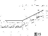
Figure 15 shows the embodiment of an electron emission display, and this electron emission display comprises wherein the barrier that forms or rib and as a plurality of electron emitting devices that are configured to a matrix form of a visual array of display.Electron emission display shown in this comprises that a preceding transparent substrates 1 and of being made by glass or suchlike material carries those electron emitting devices and supports the back substrate 10 of this preceding substrate.Be formed on back barrier or the rib RR of back in the substrate 10 and abut to form preceding barrier in the preceding substrate 1 of its top surface or rib FR so that two substrates are parallel to each other and are put separatedly, between be inserted with a vacuum space every 4.
The a plurality of Ohmic electrodes 11 that extend of being parallel to each other are formed on and approach vacuum space most on the inner surface of 4 back substrate 10.Ohmic electrode 11 is grouped into ternary some groups, and wherein three in a group are corresponding to R (red), G (green), B (indigo plant) chrominance signal, so that a color display panel to be provided, and is provided with prearranged signal separately.At Ohmic electrode 11, a plurality of electron emitting devices " S " are formed and are configured to a matrix form.On the part of the film metal electrode of neighboring devices, a plurality of perpendicular to Ohmic electrode and the bus electrode 16 that is parallel to each other by alignment to be electrically connected these film metal electrodes.Intersecting of one Ohmic electrode 11 and a bus electrode 16 corresponding to an electron emitting device " S ".Therefore, can provide a passive matrix approach or an active matrix scheme as a drive scheme that is used for display device of the present invention.
As shown in Figure 16, each electron emitting device " S " comprises that an electronics that is formed on successively on the Ohmic electrode 11 provides layer 12, one insulator layer 13 and a film metal electrode 15.Insulator layer 13 and film metal electrode 15 have a plurality of island-shaped area (not shown), wherein little by little reduce on the direction that the thickness of the island shape of insulator layer and film metal electrode part extends at their interface, as among Fig. 1,5,6 to 10,13 and 14 one of at least shown in.Film metal electrode 15 is faced vacuum space every 4.
Particularly, form an insulation holding components 17 also to determine a plurality of electron emission regions around each electron emitting device " S ".Insulation holding components 17 supporting bus electrodes 16, and prevent line fault.More specifically, as shown in Figure 16, insulation holding components 17 or have in the peripheral part of material this electron emitting device of the final thickness that is similar to the electron emitting device that forms except thickness in subsequent step of big resistance is pre-formed.
And in this embodiment, the back rib RR that is associated with back substrate 10 is formed on the insulation holding components 17 to charge into vacuum space every 4 from back substrate 10.These ribs RR is positioned with predetermined interval.Although in Figure 15, these ribs are formed between separately the electron emitting device " S ", and these ribs RR can be formed at bigger interval, for example, and every two or three electron emitting devices " S ".And, although in Figure 15, these ribs RR is formed continuously with the direction that is basically perpendicular to Ohmic electrode 11, and these ribs RR can be formed intermittently so that stay the upper area that comprises adjacent to the part of the preceding barrier FR that is associated with preceding substrate 1, but not shown.
Best, each rib RR makes its top surface district greater than the basal surface district that contacts with back substrate 10.In other words, each rib RR preferably is formed to have the extension on its top, and it is outstanding on the direction that is basically parallel to back substrate 10.
And, although in Figure 15, the bus electrode 16 of deposition is formed a simple linearity configuration on the film metal electrode 15 of back substrate 10, preferably substitute this linearity configuration and form these bus electrodes 16, so that the width between the film metal electrode 15 of electron emitting device that has is greater than the width on the film metal electrode.In other words, be preferably formed as bus electrode 16 so that the width between the electron emitting device greater than these the device on width.Like this, the resistance of bus electrode can be reduced.
The material that is used for Ohmic electrode 11 is Au, Pt, Al, the W or like that is generally used for the circuit of IC, and alternately, these Ohmic electrodes can be formed a three-decker of being made up of chromium, nickel and chromium layer.And the alloy of Al-Nd, Al-Mo or Ti-N can be used to ohmic electrode material.Ohmic electrode 11 has homogeneous thickness, is used to provide essentially identical electric current to install to each.And, by for example SiO
2, SiN
x, Al
2O
3Or the insulator of AlN forms a supplementary insulation body layer and can be set between back substrate 10 and the Ohmic electrode 11, but not shown in Figure 15.This supplementary insulation body layer is used to prevent the adverse effect (for example elutriation of the impurity of alkaline components or coarse substrate surface) of the back substrate 10 on this device.
From the principle of electronics emission, the material that is used for film metal electrode 15 have lower work function φ and thinner be preferably.For improving electronic transmitting efficiency, the material that is used for film metal electrode 15 should be the I of family of periodic table or the metal among the II of family; For example Cs, Rb, Li, Sr, Mg, Ba, Ca and like that be effectively and the alloy of these elements also can be used.For making film metal electrode 15 very thin, the material that is used for film metal electrode 15 should be have high conductivity chemically stable; For example, the single material of Au, Pt, Lu, Ag, Cu and Ir or their alloy or their multilayer are desirable.On these metals or interior coating or the doping metal that has a low work function be effective.
The material that is used for bus electrode 16 is generally used for Au, Pt, the Al or like that of the circuit of integrated circuit (IC), and should have and be enough to provide the thickness of essentially identical current potential to each device, is equivalent to 0.1 to 50 μ m.If the resistance of the material of film metal electrode can allow to be used for bus electrode, these electrode materials can be used to bus electrode.
On the other hand, be applied on the inner surface that a high-tension transparent collector 2 of being made by ITO is formed integrally on substrate 1 before the optical clear of being made by clear glass and be used as a display surface (with respect to the surface of back substrate 10).Under the situation before a secret note mask or veneer (back) metal level are set in the substrate 1, such conductive layer can be used as a collector electrode that substitutes the ITO transparent collector.
On collector electrode 2, a plurality of preceding ribs (the second insulation rib) FR is formed abreast with Ohmic electrode 11.On the collector electrode 2 between the preceding rib that extends, relatively formed every 4 with vacuum space respectively by the fluorescent material layer 3R, the 3G that make corresponding to the fluorescent material of R, G, B, 3B.Like this, preceding rib (the second insulation rib) FR is set on the border of fluorescent material separately to keep the constant distance (for example 1mm) between back substrate and the preceding substrate.Because preceding rib (the second insulation rib) FR with the direction that is deposited on back rib (the first insulation rib) quadrature in the substrate 10 of back on be configured in before in the substrate 1, substrate is by painted clearly corresponding to the fluorescent material quilt of trichromatic R, the G of light, B before guaranteeing.
As mentioned above, have a visual array of display of being made up of a plurality of light-emitting pixels according to the electron emitting device of this embodiment, these light-emitting pixels are configured to a matrix form and each light-emitting pixels comprises red (R), green (G) and blue (B) light-emitting element.Nature can form a monochromatic display floater by replace all RGB light-emitting elements with monochromatic light-emitting element.
Figure 17 shows electronics emission light-emitting device 30 according to another embodiment of the present invention, it is configured in mode similar to the aforementioned embodiment: form an Ohmic electrode 11 on a back substrate of glass 10, on electrode 11, form an electronics of making by semi-conducting material layer 12 is provided, a plurality of molecules 20 are ejected into electronics to be provided on the layer 12, and is depositing an insulator layer 13 on the layer 12 and forming a film metal electrode 15 to form a plurality of island-shaped areas 14 on layer 13.Substituting at electronics provides layer 12 to set up molecule 20, can be formed as described above as shown in Figure 8 line or anti-circular cone 21a of wall shape or the anti-circular cone 21b of column as shown in figure 10.
This electronics emission light-emitting device comprises that one is formed on the film metal electrode 15 of electron emitting device " S " and the fluorescent material layer 3 on a plurality of island-shaped area 14.This fluorescence coating 3 is directly accepted the electronics from a plurality of island-shaped areas 14 of this electron emitting device, thereby luminous.And Fig. 8 illustrates according to another electronics emission light-emitting device 30 of the present invention, and is its molecule 20 except the foregoing description is removed, same as the previously described embodiments.This electronics emission light-emitting device also comprises a derivative, and this derivative comprises the electron emitting device shown in Figure 14 and is formed on a fluorescent material layer 3 on the island-shaped area of a plurality of smooth or convexities.
The preparation method of this fluorescent material layer is that rotation applies, and wherein film metal electrode 15 is coated with the fluorescent material of colourama of the launched expectation of fluid form.The preparation method of fluorescent material layer 3 is unrestricted.
And the substrate 1 of the permeable light of being made by glass can be provided for this electronics emission light-emitting device and be formed on the suprabasil device in back as preceding substrate with protection.On the inner surface of preceding substrate, can form the collector electrode of at least one permeable light.The electronics by fluorescent material layer is captured and collected to this transparent collector electrode.Before and the back substrate use in one way by a spacer rings around binding material and be supported and sealed to face mutually, this electronics emission light-emitting device is inserted in therebetween.
According to electronics emission light-emitting device of the present invention with said structure, because fluorescent material layer is formed on the film metal electrode of electron emitting device, do not need to be used for the extra electrical power of accelerated electron, so that can in this display unit, use simple drive circuit.And since between fluorescent material layer and film metal electrode, do not have vacuum space every, by adopt electronics of the present invention emission light-emitting device can obtain a ultra-thin flat panel display unit and since do not need to be used for a vacuum space every extra spacer, such display apparatus has the good visual field of seeing from the outside.