CN1198385C - System and method for producing amplifying signals - Google Patents
System and method for producing amplifying signals Download PDFInfo
- Publication number
- CN1198385C CN1198385C CNB001285513A CN00128551A CN1198385C CN 1198385 C CN1198385 C CN 1198385C CN B001285513 A CNB001285513 A CN B001285513A CN 00128551 A CN00128551 A CN 00128551A CN 1198385 C CN1198385 C CN 1198385C
- Authority
- CN
- China
- Prior art keywords
- signal
- amplifier
- amplification
- threshold value
- amplifying
- Prior art date
- Legal status (The legal status is an assumption and is not a legal conclusion. Google has not performed a legal analysis and makes no representation as to the accuracy of the status listed.)
- Expired - Fee Related
Links
- 238000004519 manufacturing process Methods 0.000 title 1
- 238000000354 decomposition reaction Methods 0.000 claims abstract description 20
- 230000003321 amplification Effects 0.000 claims abstract description 17
- 238000003199 nucleic acid amplification method Methods 0.000 claims abstract description 17
- 238000000034 method Methods 0.000 claims description 18
- 238000006243 chemical reaction Methods 0.000 claims description 3
- 238000005516 engineering process Methods 0.000 description 6
- 238000012546 transfer Methods 0.000 description 4
- 238000004891 communication Methods 0.000 description 3
- 230000000873 masking effect Effects 0.000 description 3
- 238000012545 processing Methods 0.000 description 3
- 238000000926 separation method Methods 0.000 description 3
- 238000001228 spectrum Methods 0.000 description 3
- 239000000654 additive Substances 0.000 description 2
- 230000000996 additive effect Effects 0.000 description 2
- 238000012937 correction Methods 0.000 description 2
- 229920006395 saturated elastomer Polymers 0.000 description 2
- 238000013459 approach Methods 0.000 description 1
- 230000005540 biological transmission Effects 0.000 description 1
- 238000005422 blasting Methods 0.000 description 1
- 239000006227 byproduct Substances 0.000 description 1
- 230000001413 cellular effect Effects 0.000 description 1
- 239000002131 composite material Substances 0.000 description 1
- 239000012141 concentrate Substances 0.000 description 1
- 238000010586 diagram Methods 0.000 description 1
- 230000005669 field effect Effects 0.000 description 1
- 238000012423 maintenance Methods 0.000 description 1
- 238000012986 modification Methods 0.000 description 1
- 230000004048 modification Effects 0.000 description 1
- 238000011160 research Methods 0.000 description 1
- 238000005070 sampling Methods 0.000 description 1
- 238000004088 simulation Methods 0.000 description 1
- 230000003068 static effect Effects 0.000 description 1
Images

Classifications
-
- H—ELECTRICITY
- H03—ELECTRONIC CIRCUITRY
- H03F—AMPLIFIERS
- H03F3/00—Amplifiers with only discharge tubes or only semiconductor devices as amplifying elements
- H03F3/60—Amplifiers in which coupling networks have distributed constants, e.g. with waveguide resonators
- H03F3/602—Combinations of several amplifiers
-
- H—ELECTRICITY
- H03—ELECTRONIC CIRCUITRY
- H03F—AMPLIFIERS
- H03F3/00—Amplifiers with only discharge tubes or only semiconductor devices as amplifying elements
- H03F3/20—Power amplifiers, e.g. Class B amplifiers, Class C amplifiers
- H03F3/21—Power amplifiers, e.g. Class B amplifiers, Class C amplifiers with semiconductor devices only
- H03F3/211—Power amplifiers, e.g. Class B amplifiers, Class C amplifiers with semiconductor devices only using a combination of several amplifiers
Abstract
A signal amplification system involves decomposing a signal into two or more parts, amplifying the parts and then combining the amplified parts to produce the amplified signal. The decomposition can be done such that the resulting parts have characteristics that are amenable to efficient amplification. For example, decomposition of the signal to be amplified can be done using at least one threshold. The first part of the signal to be amplified can be formed by the portion of the signal within the threshold. As such, because the first part forms a signal with a lower PAR, the first part of the signal can be amplified more efficiently than the original signal. The second part of the signal can be formed by the portion of the original signal beyond the threshold.
Description
The present invention relates to signal is amplified, more specifically say, relate to make the system and method for the efficient and/or linear amplification of signal.
Desirable power amplifier amplifies the signal of input undeformedly.Therefore, the feature of ideal power amplifier is that a linear transfer function that does not have transfer function (input signal is to output signal) discontinuous point is arranged.But in fact, the transfer function of power amplifier exists non-linear and " linearity " district.Whether power amplifier is operated in linearity or inelastic region, depends on the amplitude of input signal.In order to make power amplifier approach linear work as far as possible, power amplifier will be designed to be operated in its linear zone, and this linear zone is given by possible input signal amplitude scope.If the amplitude of input signal is operated in outside the linear zone power amplifier, so, power amplifier can bring nonlinear component or distortion to signal.When having, input signal make amplifier saturated (along with the increase of input amplitude, output amplitude does not have perceptible increase) or end (along with reducing of input amplitude, output amplitude does not have perceptible reducing) peak amplitude the time, amplifier is by blasting, and output signal is limited with nonlinear way or serious distortion.Usually, the feature of an amplifier is that a limiting threshold is arranged, and amplitude surpasses the input signal of limiting threshold, promptly is limited in the output of amplifier.Remove and make outside the distorted signals, the amplitude limit of input signal or nonlinear distortion also produce increasing again of frequency spectrum or produce the adjacent channel power (ACP) that can disturb side frequency.
In wireless communication system, the high-power amplification of the consumption of transmission usually runs into very large peak value to average power ratio (PAR).For example, in time division multiple access (TDMA) system, when amplifying with power amplifier when a plurality of carrier signals are combined, the synthetic PAR of a large amount of carrier waves is about 9-10dB.In code division multiple access (CDMA) system, the wide carrier wave of single loading 1.25MHz can have the PAR of 11.3dB.These signals must ideally amplify linearly, to avoid producing ACP.
Regrettably, the efficient of base station is inversely proportional to its linearity.Be to obtain high linearity, the biasing of amplifier will make it to be operated in category-A or " slight " AB class (work that means is more near the AB class of category-A rather than category-B).The obtainable maximum AC of category-A work is 50% to DC efficient, and class ab ammplifier is between 50 to 78.5% (latter represents the maximal efficiency of class-b amplifier) then.Special AB class work is more near category-A, and its maximal efficiency is also low more.To adopting the amplifier of field-effect transistor, the setting of operation class (of an amplifying stage) will be according to the gate voltage of control static state (invalid) drain current that applies.To category-A work, the setting of gate voltage to make invalid drain current be similar to by with the central authorities of saturation range.The biasing of class-b amplifier near or just on ending, obtain the drain current waveform of rectification.Being biased between category-A and the category-B bias point of class ab ammplifier.Below being biased in of C class A amplifier A ended.Like this, when the amplitude of input signal when certain level is following, the C class A amplifier A is dissipation energy not.
Usually, strict linear requirement in the modern age wireless communication system limits inefficient category-A or the slight AB class mode used.Therefore, a large amount of DC power are dissipated by amplifier, thereby produce the heat that must be controlled, avoid the step-down amplifier Performance And Reliability.Thus, the use of complicated heat leak and fan becomes the necessary byproduct of high linear system.Nature, these measures are added on cost, size and the weight of base station equipment.Along with the sustainable growth of wireless communication user quantity, the quantity of base station and its little, light and cheap demand of maintenance also increase thereupon.So big quantity research concentrates on the efficient of the amplifier that requires to improve these systems and other system.
For keeping a kind of acceptable level of linearity simultaneously, various linearization techniques have been used with the higher ratio of performance to price and the amplifier of high power efficiency more.Modern age, amplifier according to usage adopted forward feedback correction, to improve the linearity of main amplifier to all kinds of input patterns.The essence of forward feedback correction is to isolate the distortion that main amplifier produces on forward path.Distortion is sent to the masking amplifier on the forward path, is corrected amplifier and amplifies.The distortion on the main signal is offset in distortion on the forward path and the combination of the distortion on the main signal.Another kind of linearization technique uses predistortion.Pre-distortion technology carried out predistortion to input signal after taking into account the transfer function characteristics of amplifier before input signal is exaggerated.So, obtain the signal that is exaggerated that needs from the input signal of predistortion.These technology help to improve the efficient of amplifier, keep linear simultaneously, but want the huge peak value of energy processing signals, and it is inefficient that the operation of amplifier remains.Other linearization technique exists.For example, reduce the ratio (PAR) of the peak value of signal, but these technology are tending towards making signal to degrade to average power as various Base-Band Processing technology such as peak clippings.The reducing of PAR numerical value limited by the admissible amount that degrades.Another kind of technology is dynamically adjusted the biasing of amplifier with the input signal envelope, and high biasing is just added up when running into big peak value.Because practical difficulty is not also seen this technology of real realization.
Because potential high-peak power, the base station of CDMA, TDMA and frequency division multiple access (FDMA) is used radio frequency (RF) amplifier that is operated in the AB mode usually, and with big current offset, so that can handle these peak powers.The efficient of these amplifiers is usually less than 10%.This poor efficiency causes higher power consumption, lower global reliability and higher working temperature.Therefore, need more high efficiency power amplifier system, it can amplify the signal with potential high-peak power with linear mode.
The present invention is a kind of signal amplifying system, and it comprises a signal decomposition is two or more parts, amplifies these parts, makes up the various piece that is exaggerated then, produces the signal that is exaggerated.The decomposition of being done will make the each several part that obtains have the characteristic that is suitable for amplifying efficiently.For example, enough at least one threshold values of resolution for the treatment of amplifying signal are finished.The first that treats amplifying signal can the part of enough this signals in threshold value form.Like this, because this first forms a signal that low PAR is arranged, so the first of signal can amplify more expeditiously than original signal.The second portion of signal can the part of enough original signals outside threshold value form.Because second portion is almost nil, so second portion can amplify efficiently, for example use the C class A amplifier A, its any energy that when input signal is zero, do not dissipate.
Other aspects of the present invention and advantage, below reading detailed explanation and with reference to the accompanying drawings after, will see clearlyer.
Fig. 1 draw 40 full price users two kinds of CDMA carrier waves PAR and be set at the pilot signal power of gross power 15%;
Fig. 2 is according to the principle of the invention, the signal decomposition of drawing be within the threshold value and threshold value outside two parts; With
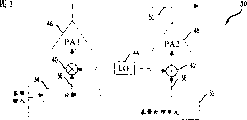
Fig. 3 is according to the principle of the invention, the amplifier system of a kind of demonstration of drawing, its with base-band digital equipment signal decomposition.
Below by each illustrative embodiment, the power amplifier scheme of utilizing the principle of the invention is described, improve the power amplification efficient of the signal that huge PAR is arranged.Fig. 1 draw the PAR curve 12 of IS-95 code division multiple access (CDMA) 1.25 megahertzes (MHz) carrier wave and the PAR curve 14 of CDMA 20001X carrier wave.Explanation about IS-95, can in standard, find as EIA/TIA/IS-95 (Electronic Industries Association/Telecommunication IndustryAssociation/Interim Standard 95) authentication, title is " MobileStation-Base Station Compatibility Standard for Dual-ModeWideband Spread Spectrum Cellular System ", March 1993 (" IS-95 ").The explanation of CDMA 2000 can be found in the standard as EIA/TIA/IS-2000, title is that " Spread Spectrum Digital Technology-Mobile and PersonalCommunications Standards. " IS-95 carrier wave and CDMA 2000 carrier wave boths are fully loaded with 40 full price users, and pilot power is 15% of a gross power.As shown in Figure 1, be 10 at the peak value probability of occurrence
-4When (referring to that the chance that certain peak value surpasses certain level of average power is 1/10,000), the have an appointment PAR of 11.3dB of the single carrier wave IS-95 carrier wave of loading, and the have an appointment PAR of 9.6dB of single carrier wave CDMA 2000 carrier waves that load.
Using certain the separation threshold value based on power level, for example surpass average power 6dB, can be signal decomposition each several part.Fig. 1 points out, with the separation threshold value that surpasses average power 6dB, CDMA 2000 signals about 98% are separating within the threshold value and are being formed with the signal section of lower PAR (approximate 6dB), and this signal has 2% to surpass threshold value and 98% the time of being formed with is a signal of zero approximately.Fig. 1 points out that also IS-95 signal about 95% separates within the threshold value and is formed with the signal section of low PAR at 6dB, and has 5% signal to surpass threshold value approximately.
The decomposition that Fig. 2 draws signal 16 with figure.In this figure, signal is as certain signal level is arranged, and as voltage level, draws according to the time, separates threshold value 20 then based on positive and negative signal level.Separate threshold value as the explanation suggestion of Fig. 1, can be based on amplitude or power level.For example, the power level of the signal of homophase (I) and two components of quadrature (Q) being arranged is V
I 2+ V
Q 2, can be based on certain power level and separate threshold value.Like this, the part of signal is being separated on the threshold value, and another part is then separating under the threshold value.Signal 16 is decomposed into the first 18 within threshold value 20.There is lower PAR in first 18, thereby can amplify more efficiently than original signal.Signal 16 also is decomposed into the second portion 22 above threshold value 20.Second portion is almost nil and can amplify efficiently with the C class A amplifier A, because when input signal is zero, and C class A amplifier A any energy that do not dissipate.Relevant with embodiment, signal 16 can be decomposed into more than two parts, and/or can be with the original signal 16 of a plurality of threshold decomposition.There is the additive method that decomposes original signal 16.For example, the one skilled in the art should be understood that the decomposition of signal can be gone up in base band, at intermediate frequency (IF) or at radio frequency (RF) and carries out described function with discrete component.Have other decomposition of original signal 16, for example first and second parts at least can be one group of part or functions that changes of original signal amplitude.
Fig. 3 a kind of programmatic block diagram of amplifier system 30 that draws is implemented to decompose on base band with digital form on it.In this embodiment, processing unit or circuit 32 be at the base band receiving digital signals, and to base-band input signal operation resolving cell 34.Resolving cell 34 decomposed signals are producing first and producing second portion on the second amplifier paths 38 on the first amplifier path 36.In this embodiment, first and second parts are distinguishing, and distinct time domain specification and/or distinct frequency domain characteristic are for example arranged.First can be original signal in threshold value with interior part, and second portion can be the part that signal surpasses threshold value.In this embodiment, second power amplifier (PA2) 48 receives the RF signal and amplifies the peak signal at intermittence that the original signal of the second amplifier path, 38 representatives surpasses threshold value from frequency mixer 42.The output of amplifier 46 (PA1) and 48 (PA2) is made up on combiner or coupler 50, forms the output signal that is exaggerated at last.Combiner or coupler 50 can be impedance matching networks, as the part of 50 ohm of networks, to keep the output impedance level of looking from amplifier 46 and 48.Amplifier 46 (PA1) and/or 48 (PA2) can be the parts of feedforward or predistortion system, or individually represent the amplifier with feedforward or predistortion linear.For example, first and/or second portion of signal can be amplified for 46 and/or 48 by predistortion.Equally, the signal that has amplified can be with feedforward linearized.Relevant with embodiment, originally signal can be decomposed into the more part on the more path, is amplified by the more power amplifier, is combined into the linear output signal that is exaggerated then.
In a kind of linearizer circuit typical, realization feedforward in analog domain, masking amplifier must be very linear amplifier.If it is obviously saturated that main amplifier occurs, can increase the efficient of main amplifier, but error signal also there is very large dynamic range.So masking amplifier is with low efficient work.In the present invention, second amplifier is with efficiency operation.In addition, in feed forward circuit, the signal that has distortion for guaranteeing to be exaggerated makes up in correct time with segregate distortion on the forward path, so that eliminate distortion, needs the RF delay line of simulation, and the present invention has no longer needed.
As an example, amplifier if desired is that to be used for average output power be 10 watts signal, the PAR of signal is 9dB after certain base band peak-limitation algorithm, and so, this amplifier must be able to be handled the peak power of 80 watts (9dB converts approximate 8 times to).With system 30, suppose that combiner 50 is directional couplers of 6dB, and to separate threshold value be to be higher than mean value 5dB, main amplifier 46 need only be handled about 42.5 watts peak power, it is higher than 10 watts of 6.25dB, has taken into account the loss 1.25dB (5dB+1.25dB=6.25dB) by combiner.The PAR of main amplifier 46 amplifying signals can calculate and is about 6.4dB, and about 2.6dB has descended.The efficient of main amplifier 46 is more high than this single amplifier.Through after the 1.25dB loss of combiner 50, can have an appointment 32 watts peak power of the first that is exaggerated.Because we need 80 watts power, booster amplifier 48 must be handled about 43.6 watts peak power after the 6dB loss of taking into account by combiner 50, here 43.6 watts peak power=
 (being about 4 times).Yet in the present embodiment, the time of second amplifier, 48 conductings is less than 5%.When conducting, the PAR of its amplifying signal can calculate and be about 4.9dB.Like this, booster amplifier can be worked very efficiently.
As a comparison, given certain way, wherein, signal is broken down into the duplicate of two original signals, each is amplified by two amplifiers, each amplifier can be handled 80 watts peak power, simply the power combination of two amplifiers, obtains an energy is sent 20 watts of average powers to the signal of 9dB PAR power amplifier.Each amplifier All Time conducting, and operate on 10 watts the average power.If with there being the 6dB coupler to separate the new system of threshold value with 5dB, this system 30 can be sent 18.3 watts average power, a little less than 20 watts of front scheme.Though main amplifier 46 moves on 17.9 watts of average powers, the dissipation of main amplifier 46 is only slightly many than a device in the aforementioned schemes, and (power dissipation when zero input power) is the main power consumption of this class A amplifier A because quiescent biasing dissipates.But, as second amplifier 48 of the booster amplifier considerably less power that dissipates, because it is only less than 5% time conducting.When its conducting, no more than another amplifier of power that it dissipates.Therefore, the efficient of system 30 is higher than general 50% at least.
In addition to the implementation, have the other configuration according to the power amplifier system of the principle of the invention, it saves and/or increases some elements, and/or with some variation or the part of said system.For example, can on the signal path before amplifier 46 and/or 48, place phase-shifter, adjust the relative phase between the each several part,, improve the combination of signal so that adjust the mismatch between the amplifier 46 and 48.Also have, coupler can be delivered to control circuit or treatment circuit 32 to the sampling of amplifying signal, so that control signal is delivered to phase-shifter, or signal is adjusted to improve performance.In addition, the embodiment of the power amplifier system that has illustrated is with special system, wherein, signal originally is to decompose in digital baseband domain, still, this decomposition also can occur on the IF or RF in the analog domain, or occurs on the IF or RF in other amplifiers or the circuit arrangement.For example, the decomposition of input signal can be finished on IF in decomposition circuit or the RF at signal after digital baseband and/or IF conversion.
, power amplifier system is illustrated, still,, and Signal Separation is become the additive method of different piece, also can finish decomposition with threshold value a plurality of and/or variation according to separating threshold value signal decomposition.The system that has illustrated uses coupler that each several part is made up, but other composite sets also can use as adder or combiner.Along with different application, decompose and/or power amplification circuit, can be used in or add to feedforward, predistortion or other linearisations or improve the technical of efficient.Power amplifying system is also according to the difference configuration of using discrete component, further be illustrated, but should be understood that, disclosure by this paper, this area general skilled person should be understood that, other of integrated circuit, software-driven treatment circuit, firmware or the discrete component that feedforward system and part feedforward system can application specific are arranged and realized.All that illustrate are only for showing the application of the principles of the present invention.The one skilled in the art discerns easily, need not strictness and defers to the example use of demonstrating and illustrating here, also need not to depart from the spirit and scope of the present invention, can make these or other various modification of the present invention, device or method.
Claims (11)
1. method that produces amplifying signal, the feature of described method is:
At least use a limiting threshold, treating that amplifying signal (16) is decomposed into first (18) and second portion (22) at least, wherein, the signal section that first comprises, ratio is a based signal with the limiting threshold, the ratio of lower peak value to average power is arranged, and second portion comprises the signal section that surpasses limiting threshold;
Amplify described described first (18) and described second portion (22) at least, so that produce the first of amplification at least and the second portion of amplification; With
The second portion of the first of described described amplification at least and described amplification is combined, produce an amplifying signal.
2. according to the method for claim 1, it is characterized in that described decomposition also comprises:
Provide the described first (18) of described signal (16), as the part of described signal in described threshold value (20); With
The described second portion (22) of described signal is provided, surpasses the part of described threshold value (20) as described signal (16).
3. according to the method for claim 2, it is characterized in that described decomposition comprises:
Detect the amplitude of described signal; With
The described amplitude of described signal and described threshold value (20) are compared.
4. according to the method for claim 2, it is characterized in that described amplification comprises:
Amplify described first (18) with first amplifier (46); With
Amplify described second portion (22) with second amplifier (48).
5. according to the method for claim 2, its feature also is:
Before amplification, described first (18) is carried out up-conversion; With
Before amplification, described second portion (22) is carried out up-conversion.
6. according to the method for claim 2, it is characterized in that the described described first (18) that provides comprises:
The described first (18) that provides compares with described signal (16), the peak value that reduces is arranged to average power ratio.
7. according to the method for claim 1, it is characterized in that described combination comprises:
Use the matched impedance network, make up described first (18) and described second portion (22).
8. according to the method for claim 7, it is characterized in that described use comprises:
Use directional coupler (50), make up described first (18) and described second portion (22).
9. according to the method for claim 3, it is characterized in that described decomposition comprises:
In baseband digital domain, finish the described decomposition of described signal.
10. a signal amplifying system (30) is characterized in that:
Circuit (32), be configured to decompose and treat amplifying signal, and go up generation first (18) in first path (36) at least, with last according at least one limiting threshold, produce second portion, wherein in second path (38), the signal section that first comprises, than being based signal, the ratio of lower peak value to average power is arranged, and second portion comprises the signal section that surpasses limiting threshold with the limiting threshold;
First amplifier (46) on described first path (36) receives described first (18) and amplifies described first, produces the first of amplifying;
Second amplifier (48) on described second path (38) receives described second portion (22) and amplifies described second portion (22), produces the second portion that amplifies; With
Combinational circuit (50) is configured to receive the first of described amplification and the second portion of described amplification, and makes up the first of described amplification and the second portion of described amplification, produces an amplifying signal.
11. system according to claim 10, it is characterized in that, the configuration of described circuit (32), want and to compare the amplitude of described signal (16) and described threshold value (20), and produce described signal in described threshold value (20) with interior part, as described first (18), also produce the part that described signal (16) surpasses described threshold value (20), as described second portion (22).
Applications Claiming Priority (2)
| Application Number | Priority Date | Filing Date | Title |
|---|---|---|---|
| US09/444,319 US6292054B1 (en) | 1999-11-19 | 1999-11-19 | System and method for producing an amplified signal |
| US09/444,319 | 1999-11-19 |
Publications (2)
| Publication Number | Publication Date |
|---|---|
| CN1299186A CN1299186A (en) | 2001-06-13 |
| CN1198385C true CN1198385C (en) | 2005-04-20 |
Family
ID=23764413
Family Applications (1)
| Application Number | Title | Priority Date | Filing Date |
|---|---|---|---|
| CNB001285513A Expired - Fee Related CN1198385C (en) | 1999-11-19 | 2000-11-17 | System and method for producing amplifying signals |
Country Status (8)
| Country | Link |
|---|---|
| US (2) | US6292054B1 (en) |
| EP (1) | EP1102393A3 (en) |
| JP (1) | JP2001189630A (en) |
| KR (1) | KR20010051821A (en) |
| CN (1) | CN1198385C (en) |
| AU (1) | AU769523B2 (en) |
| BR (1) | BR0005431A (en) |
| CA (1) | CA2324846C (en) |
Families Citing this family (27)
| Publication number | Priority date | Publication date | Assignee | Title |
|---|---|---|---|---|
| GB0020071D0 (en) * | 2000-08-16 | 2000-10-04 | Mitel Semiconductor Ltd | Tuner |
| GB0110106D0 (en) * | 2001-04-25 | 2001-06-20 | Filtronic Plc | Electrical signal preconditioning |
| US6891902B2 (en) * | 2002-07-02 | 2005-05-10 | Intel Corporation | System and method for adjusting a power level of a transmission signal |
| FI115935B (en) | 2003-02-25 | 2005-08-15 | Nokia Corp | Method and apparatus for regulating amplifier characteristics |
| US7197086B2 (en) * | 2003-05-29 | 2007-03-27 | Lucent Technologies Inc. | Wide-bandwidth, high-dynamic-range linear amplifier for a CDMA transmitter in a wireless base station |
| KR101009778B1 (en) * | 2003-10-23 | 2011-01-19 | 삼성전자주식회사 | Apparatus and method for amplifing power under a large peak-to-average ratio |
| US7327803B2 (en) | 2004-10-22 | 2008-02-05 | Parkervision, Inc. | Systems and methods for vector power amplification |
| US7355470B2 (en) | 2006-04-24 | 2008-04-08 | Parkervision, Inc. | Systems and methods of RF power transmission, modulation, and amplification, including embodiments for amplifier class transitioning |
| US7148746B2 (en) * | 2004-10-26 | 2006-12-12 | Andrew Corporation | High efficiency amplifier |
| US7911272B2 (en) | 2007-06-19 | 2011-03-22 | Parkervision, Inc. | Systems and methods of RF power transmission, modulation, and amplification, including blended control embodiments |
| US8334722B2 (en) | 2007-06-28 | 2012-12-18 | Parkervision, Inc. | Systems and methods of RF power transmission, modulation and amplification |
| US7856105B2 (en) * | 2006-03-09 | 2010-12-21 | Andrew Llc | Apparatus and method for processing of amplifier linearization signals |
| JP4646845B2 (en) * | 2006-03-30 | 2011-03-09 | 富士通株式会社 | Transmitter |
| US7937106B2 (en) | 2006-04-24 | 2011-05-03 | ParkerVision, Inc, | Systems and methods of RF power transmission, modulation, and amplification, including architectural embodiments of same |
| US8031804B2 (en) | 2006-04-24 | 2011-10-04 | Parkervision, Inc. | Systems and methods of RF tower transmission, modulation, and amplification, including embodiments for compensating for waveform distortion |
| US8315336B2 (en) | 2007-05-18 | 2012-11-20 | Parkervision, Inc. | Systems and methods of RF power transmission, modulation, and amplification, including a switching stage embodiment |
| JP4653724B2 (en) * | 2006-11-30 | 2011-03-16 | 富士通株式会社 | Transmitter that suppresses signal out-of-band power |
| WO2008156800A1 (en) | 2007-06-19 | 2008-12-24 | Parkervision, Inc. | Combiner-less multiple input single output (miso) amplification with blended control |
| WO2009145887A1 (en) | 2008-05-27 | 2009-12-03 | Parkervision, Inc. | Systems and methods of rf power transmission, modulation, and amplification |
| US8315578B2 (en) * | 2008-07-15 | 2012-11-20 | Research In Motion Limited | Mobile wireless communications device with separate in-phase and quadrature power amplification |
| WO2012139126A1 (en) | 2011-04-08 | 2012-10-11 | Parkervision, Inc. | Systems and methods of rf power transmission, modulation, and amplification |
| WO2012167111A2 (en) | 2011-06-02 | 2012-12-06 | Parkervision, Inc. | Antenna control |
| KR20160058855A (en) | 2013-09-17 | 2016-05-25 | 파커비전, 인크. | Method, apparatus and system for rendering an information bearing function of time |
| CN107005201A (en) * | 2014-12-02 | 2017-08-01 | 华为技术有限公司 | Amplification system for amplifying signal of communication |
| KR101952875B1 (en) | 2017-08-24 | 2019-05-23 | 삼성전기주식회사 | Power amplifier and integrated circuit comprising the same |
| JP6925561B2 (en) * | 2019-02-26 | 2021-08-25 | 三菱電機株式会社 | Directional couplers and semiconductor chips |
| CN111654243B (en) * | 2019-03-04 | 2023-03-03 | 华为技术有限公司 | Power amplification device, beam forming system, transmitter and base station |
Family Cites Families (12)
| Publication number | Priority date | Publication date | Assignee | Title |
|---|---|---|---|---|
| DE2701463A1 (en) * | 1977-01-14 | 1978-07-20 | Hoeglund Lennart H E | Amplifier circuit with parallel amplifier stages - includes amplifying element and two gates blocking passage of signal outside threshold values |
| US4283685A (en) * | 1979-12-13 | 1981-08-11 | Raytheon Company | Waveguide-to-cylindrical array transition |
| US4748421A (en) * | 1987-04-08 | 1988-05-31 | Scs Telecom, Inc. | Enhanced class SM power amplifier |
| US5101171A (en) * | 1990-11-23 | 1992-03-31 | Advanced Systems Research, Inc. | Extended bandwidth RF amplifier |
| US5262958A (en) * | 1991-04-05 | 1993-11-16 | Texas Instruments Incorporated | Spline-wavelet signal analyzers and methods for processing signals |
| US5278912A (en) * | 1991-06-28 | 1994-01-11 | Resound Corporation | Multiband programmable compression system |
| FR2701796A1 (en) * | 1993-02-17 | 1994-08-26 | Philips Electronics Nv | Device for the transmission of television signals. |
| US5822370A (en) * | 1996-04-16 | 1998-10-13 | Aura Systems, Inc. | Compression/decompression for preservation of high fidelity speech quality at low bandwidth |
| KR100266817B1 (en) * | 1997-01-31 | 2000-09-15 | 윤종용 | Apparatus and method for amplifying tx signal in linear power amplifier using feed forward |
| US6085074A (en) * | 1997-02-28 | 2000-07-04 | Motorola, Inc. | Apparatus and method for amplifying an amplitude-varying signal |
| US5886573A (en) * | 1998-03-06 | 1999-03-23 | Fujant, Inc. | Amplification using amplitude reconstruction of amplitude and/or angle modulated carrier |
| US6054894A (en) * | 1998-06-19 | 2000-04-25 | Datum Telegraphic Inc. | Digital control of a linc linear power amplifier |
-
1999
- 1999-11-19 US US09/444,319 patent/US6292054B1/en not_active Expired - Lifetime
-
2000
- 2000-10-31 CA CA002324846A patent/CA2324846C/en not_active Expired - Fee Related
- 2000-11-06 EP EP00309801A patent/EP1102393A3/en not_active Withdrawn
- 2000-11-10 AU AU71536/00A patent/AU769523B2/en not_active Ceased
- 2000-11-17 CN CNB001285513A patent/CN1198385C/en not_active Expired - Fee Related
- 2000-11-17 JP JP2000350488A patent/JP2001189630A/en not_active Abandoned
- 2000-11-17 BR BR0005431-3A patent/BR0005431A/en not_active IP Right Cessation
- 2000-11-20 KR KR1020000068994A patent/KR20010051821A/en not_active Application Discontinuation
-
2001
- 2001-05-10 US US09/852,990 patent/US6624694B2/en not_active Expired - Lifetime
Also Published As
| Publication number | Publication date |
|---|---|
| US6292054B1 (en) | 2001-09-18 |
| KR20010051821A (en) | 2001-06-25 |
| US20010035791A1 (en) | 2001-11-01 |
| EP1102393A2 (en) | 2001-05-23 |
| CA2324846C (en) | 2003-03-18 |
| CA2324846A1 (en) | 2001-05-19 |
| US6624694B2 (en) | 2003-09-23 |
| CN1299186A (en) | 2001-06-13 |
| AU769523B2 (en) | 2004-01-29 |
| BR0005431A (en) | 2001-08-07 |
| AU7153600A (en) | 2001-05-24 |
| EP1102393A3 (en) | 2004-06-30 |
| JP2001189630A (en) | 2001-07-10 |
Similar Documents
| Publication | Publication Date | Title |
|---|---|---|
| CN1198385C (en) | System and method for producing amplifying signals | |
| CA2234335C (en) | High efficiency power amplifier | |
| AU776377B2 (en) | Power amplifier using upstream signal information | |
| US7339426B2 (en) | High efficiency linear amplifier employing dynamically controlled back off | |
| US7440733B2 (en) | Constant gain nonlinear envelope tracking high efficiency linear amplifier | |
| US7038539B2 (en) | RF amplifier employing active load linearization | |
| US8013676B2 (en) | High-efficiency power amplifier | |
| EP1583227A1 (en) | Doherty amplifier | |
| EP1714383A1 (en) | Methods and systems for signal amplification through envelope removal and restoration | |
| CN101114811A (en) | Analog predistortion based linear power amplification circuit and method | |
| Ranjan et al. | Microwave power amplifiers with digitally-controlled power supply voltage for high efficiency and high linearity | |
| JPWO2009066353A1 (en) | Power amplifier | |
| Darraji et al. | Generic load-pull-based design methodology for performance optimisation of Doherty amplifiers | |
| Woo et al. | Predistortion linearization system for high power amplifiers | |
| KR101686351B1 (en) | 3-way doherty power amplifier | |
| CN115882795B (en) | Power amplifier with linearization compensation structure | |
| KR20040106018A (en) | Analog adaptive predistorter for power amplifier | |
| Kim et al. | 1.9 GHz band highly linear 2-stage power amplifier MMIC based on InGaP/GaAs HBT | |
| KR20080023773A (en) | Predistorter to compensate for am-to-am and am-to-pm in the power amplifier | |
| Aniktar et al. | HIGHLY LINEAR RF POWER AMPLIFIER DESIGN | |
| Zhang et al. | Low cost solution to enhance performance of CDMA repeater amplifier | |
| KR20140084861A (en) | Doherty amplifier with smaller size and extended bandwidth | |
| CN116781017A (en) | Compact Doherty power amplifier applied to 5G communication | |
| Morris et al. | Reducing feed-through effect within envelope elimination and restoration transmitters | |
| Iizuka et al. | High-efficiency Doherty linear amplifier with backoff control for mobile communications |
Legal Events
| Date | Code | Title | Description |
|---|---|---|---|
| C06 | Publication | ||
| PB01 | Publication | ||
| C10 | Entry into substantive examination | ||
| SE01 | Entry into force of request for substantive examination | ||
| C14 | Grant of patent or utility model | ||
| GR01 | Patent grant | ||
| CF01 | Termination of patent right due to non-payment of annual fee |
Granted publication date: 20050420 Termination date: 20161117 |
|
| CF01 | Termination of patent right due to non-payment of annual fee |