CN115346451A - Box body assembly and display screen - Google Patents
Box body assembly and display screen Download PDFInfo
- Publication number
- CN115346451A CN115346451A CN202210999356.5A CN202210999356A CN115346451A CN 115346451 A CN115346451 A CN 115346451A CN 202210999356 A CN202210999356 A CN 202210999356A CN 115346451 A CN115346451 A CN 115346451A
- Authority
- CN
- China
- Prior art keywords
- section
- unit
- units
- adjacent
- profile
- Prior art date
- Legal status (The legal status is an assumption and is not a legal conclusion. Google has not performed a legal analysis and makes no representation as to the accuracy of the status listed.)
- Granted
Links
- 238000009434 installation Methods 0.000 claims description 21
- 229910052751 metal Inorganic materials 0.000 claims description 5
- 239000002184 metal Substances 0.000 claims description 5
- 238000000034 method Methods 0.000 abstract description 8
- 230000009286 beneficial effect Effects 0.000 abstract description 6
- 238000003466 welding Methods 0.000 description 9
- 238000010586 diagram Methods 0.000 description 8
- 239000000463 material Substances 0.000 description 8
- 238000003780 insertion Methods 0.000 description 7
- 230000037431 insertion Effects 0.000 description 7
- 239000011295 pitch Substances 0.000 description 7
- 238000013461 design Methods 0.000 description 6
- 230000000694 effects Effects 0.000 description 5
- 238000004512 die casting Methods 0.000 description 4
- 238000012545 processing Methods 0.000 description 4
- 230000004308 accommodation Effects 0.000 description 2
- 229910052782 aluminium Inorganic materials 0.000 description 2
- XAGFODPZIPBFFR-UHFFFAOYSA-N aluminium Chemical compound [Al] XAGFODPZIPBFFR-UHFFFAOYSA-N 0.000 description 2
- 230000004927 fusion Effects 0.000 description 2
- 230000017525 heat dissipation Effects 0.000 description 2
- 238000012966 insertion method Methods 0.000 description 2
- 229910000679 solder Inorganic materials 0.000 description 2
- 102100027730 Endogenous retrovirus group K member 19 Rec protein Human genes 0.000 description 1
- 101001064123 Homo sapiens Endogenous retrovirus group K member 19 Env polyprotein Proteins 0.000 description 1
- 101000893974 Homo sapiens Endogenous retrovirus group K member 19 Gag polyprotein Proteins 0.000 description 1
- 101000956190 Homo sapiens Endogenous retrovirus group K member 19 Pro protein Proteins 0.000 description 1
- 101000580915 Homo sapiens Endogenous retrovirus group K member 19 Rec protein Proteins 0.000 description 1
- 101001066689 Homo sapiens Integrase Proteins 0.000 description 1
- 239000000853 adhesive Substances 0.000 description 1
- 230000001070 adhesive effect Effects 0.000 description 1
- 238000005452 bending Methods 0.000 description 1
- 238000005516 engineering process Methods 0.000 description 1
- 230000010354 integration Effects 0.000 description 1
- 238000005304 joining Methods 0.000 description 1
- 238000003754 machining Methods 0.000 description 1
- 238000012986 modification Methods 0.000 description 1
- 230000004048 modification Effects 0.000 description 1
Images



Classifications
-
- G—PHYSICS
- G09—EDUCATION; CRYPTOGRAPHY; DISPLAY; ADVERTISING; SEALS
- G09F—DISPLAYING; ADVERTISING; SIGNS; LABELS OR NAME-PLATES; SEALS
- G09F9/00—Indicating arrangements for variable information in which the information is built-up on a support by selection or combination of individual elements
- G09F9/30—Indicating arrangements for variable information in which the information is built-up on a support by selection or combination of individual elements in which the desired character or characters are formed by combining individual elements
- G09F9/33—Indicating arrangements for variable information in which the information is built-up on a support by selection or combination of individual elements in which the desired character or characters are formed by combining individual elements being semiconductor devices, e.g. diodes
-
- G—PHYSICS
- G09—EDUCATION; CRYPTOGRAPHY; DISPLAY; ADVERTISING; SEALS
- G09F—DISPLAYING; ADVERTISING; SIGNS; LABELS OR NAME-PLATES; SEALS
- G09F9/00—Indicating arrangements for variable information in which the information is built-up on a support by selection or combination of individual elements
- G09F9/30—Indicating arrangements for variable information in which the information is built-up on a support by selection or combination of individual elements in which the desired character or characters are formed by combining individual elements
- G09F9/302—Indicating arrangements for variable information in which the information is built-up on a support by selection or combination of individual elements in which the desired character or characters are formed by combining individual elements characterised by the form or geometrical disposition of the individual elements
- G09F9/3026—Video wall, i.e. stackable semiconductor matrix display modules
-
- H—ELECTRICITY
- H05—ELECTRIC TECHNIQUES NOT OTHERWISE PROVIDED FOR
- H05K—PRINTED CIRCUITS; CASINGS OR CONSTRUCTIONAL DETAILS OF ELECTRIC APPARATUS; MANUFACTURE OF ASSEMBLAGES OF ELECTRICAL COMPONENTS
- H05K5/00—Casings, cabinets or drawers for electric apparatus
- H05K5/0017—Casings, cabinets or drawers for electric apparatus with operator interface units
-
- H—ELECTRICITY
- H05—ELECTRIC TECHNIQUES NOT OTHERWISE PROVIDED FOR
- H05K—PRINTED CIRCUITS; CASINGS OR CONSTRUCTIONAL DETAILS OF ELECTRIC APPARATUS; MANUFACTURE OF ASSEMBLAGES OF ELECTRICAL COMPONENTS
- H05K5/00—Casings, cabinets or drawers for electric apparatus
- H05K5/02—Details
- H05K5/0217—Mechanical details of casings
Landscapes
- Engineering & Computer Science (AREA)
- Microelectronics & Electronic Packaging (AREA)
- Physics & Mathematics (AREA)
- General Physics & Mathematics (AREA)
- Theoretical Computer Science (AREA)
- Devices For Indicating Variable Information By Combining Individual Elements (AREA)
- Multimedia (AREA)
Abstract
本发明提供了一种箱体组件及显示屏,箱体组件包括:两个以上型材单元,型材单元之间沿型材单元的宽度方向依次排列,其中,相邻两个所述型材单元中的一个设有导向结构,所述导向结构与另一个所述型材单元配合使得相邻两个所述型材单元能拼合在一起,并且相邻两个所述型材单元在拼合处焊接成一体。本发明提供的箱体组件,在组装过程中通过导向结构对正两个型材单元,使得型材单元之间能够保障较高的位置精度,在将对正后的两个型材单元焊接成一体,利于保障显示屏的平度面。

The invention provides a box assembly and a display screen. The box assembly includes: more than two profile units, and the profile units are arranged in sequence along the width direction of the profile units, wherein one of the two adjacent profile units A guide structure is provided, and the guide structure cooperates with another profile unit so that two adjacent profile units can be joined together, and the two adjacent profile units are welded together at the joint. The box assembly provided by the present invention aligns the two profile units through the guide structure during the assembly process, so that a high positional accuracy can be ensured between the profile units, and the aligned two profile units are welded into one body, which is beneficial Ensure the flat surface of the display.
Description
技术领域technical field
本发明涉及显示屏领域,特别涉及一种箱体组件及一种显示屏。The invention relates to the field of display screens, in particular to a box assembly and a display screen.
背景技术Background technique
LED显示屏的箱体,通常由多个标准压铸箱体拼接形成,相邻的标准压铸箱体之间通过紧固件固定。由于采用通用标准压铸箱体,箱体尺寸普遍较小,这样的话物料的种类和数量就会相对比较零碎、偏多,拼装位置多、组装环节偏长,装配偏差较大。The cabinet of the LED display is usually formed by splicing multiple standard die-casting cabinets, and the adjacent standard die-casting cabinets are fixed by fasteners. Due to the use of general standard die-casting cabinets, the size of the cabinets is generally small, so the types and quantities of materials will be relatively fragmented, too many, there are many assembly positions, the assembly process is too long, and the assembly deviation is large.
发明内容Contents of the invention
本发明的一个目的在于提出一种箱体组件,其通过较大尺寸的型材单元拼装形成,实现减少物料数量和种类,减少了拼装步骤,提升了装配精度。An object of the present invention is to provide a box assembly, which is formed by assembling large-sized profile units, so as to reduce the quantity and types of materials, reduce assembling steps, and improve assembly accuracy.
为解决上述技术问题,本发明采用如下技术方案:In order to solve the problems of the technologies described above, the present invention adopts the following technical solutions:
本发明的技术方案提出了一种箱体组件,用于显示屏,包括:The technical solution of the present invention proposes a box assembly for a display screen, including:
两个以上型材单元,所述型材单元之间沿所述型材单元的宽度方向依次排列,其中,相邻两个所述型材单元中的一个设有导向结构,所述导向结构与另一个所述型材单元配合使得相邻两个所述型材单元能拼合在一起,并且相邻两个所述型材单元在拼合处焊接成一体。More than two profile units, the profile units are arranged in sequence along the width direction of the profile units, wherein, one of the two adjacent profile units is provided with a guide structure, and the guide structure is connected to the other of the profile units. The fit of the profile units enables two adjacent profile units to be spliced together, and the two adjacent profile units are welded together at the joint.
根据本发明的一些技术方案,至少部分所述型材单元的宽度方向的两端分别形成有拼接侧面,相邻所述型材单元的所述拼接侧面相焊接;According to some technical solutions of the present invention, splicing sides are respectively formed at both ends in the width direction of at least part of the profile units, and the splicing sides of adjacent profile units are welded;
所述型材单元的一个所述拼接侧面上设有所述导向结构,所述型材单元的所述导向结构和与之相邻的所述型材单元的所述拼接侧面相连,使相邻两个所述型材单元在所述型材单元的厚度方向和/或长度方向上被定位。The guide structure is provided on one splicing side of the profile unit, and the guide structure of the profile unit is connected to the splicing side of the adjacent profile unit, so that two adjacent The profile unit is positioned in the thickness direction and/or the length direction of the profile unit.
根据本发明的一些技术方案,所述导向结构包括插接部,所述型材单元的一个所述拼接侧面上设置有所述插接部,所述型材单元的所述插接部和与之相邻的所述型材单元的所述拼接侧面相连,使相邻两个所述型材单元在所述型材单元的厚度方向和/或长度方向上被定位。According to some technical solutions of the present invention, the guide structure includes an insertion part, the insertion part is provided on one of the splicing sides of the profile unit, and the insertion part of the profile unit is connected to it. The joining sides of the adjacent profile units are connected so that two adjacent profile units are positioned in the thickness direction and/or the length direction of the profile units.
根据本发明的一些技术方案,所述插接部包括插入件,所述型材单元的一个所述拼接侧面上设置有多个所述插入件,多个所述插入件之间沿所述型材单元的长度方向间隔排布;According to some technical solutions of the present invention, the insertion part includes an insert, and a plurality of inserts are provided on one splicing side of the profile unit, and a plurality of inserts are arranged along the profile unit. Arranged at intervals in the length direction;
所述型材单元的另一个所述拼接侧面上形成有多个凹槽,多个所述凹槽和多个所述插入件一对一地排布,所述型材单元的所述插入件插入与之相邻的所述型材单元的所述凹槽,使相邻两个所述型材单元在所述型材单元的长度方向上被定位。A plurality of grooves are formed on the other splicing side of the profile unit, and a plurality of the grooves and a plurality of inserts are arranged one-to-one, and the inserts of the profile unit are inserted into the The grooves of the adjacent profile units allow two adjacent profile units to be positioned in the length direction of the profile units.
根据本发明的一些技术方案,所述型材单元设有第一连接结构,所述第一连接结构用于与显示模组的第二连接结构相连,以使所述显示模组装配于所述型材单元上,其中,所述第一连接结构和所述第二连接结构中的一个为磁吸结构,另一个为能与所述磁吸结构磁吸连接的金属件。According to some technical solutions of the present invention, the profile unit is provided with a first connection structure, and the first connection structure is used to connect with the second connection structure of the display module, so that the display module is assembled on the profile On the unit, one of the first connection structure and the second connection structure is a magnetic attraction structure, and the other is a metal piece capable of magnetically attracting connection with the magnetic attraction structure.
根据本发明的一些技术方案,每个所述型材单元包括至少两个子型材,所述子型材之间沿所述型材单元的宽度方向并排设置并和与之相邻的所述子型材焊接成一体。According to some technical solutions of the present invention, each of the profile units includes at least two sub-profiles, and the sub-profiles are arranged side by side along the width direction of the profile unit and welded together with the adjacent sub-profiles .
根据本发明的一些技术方案,所述型材单元具有位置相对且间隔的背板和前板,所述拼接侧面衔接所述背板和所述前板,使所述背板、所述前板和所述拼接侧面共同限定出能用于容纳电控部件的容纳空间。According to some technical solutions of the present invention, the profile unit has a back plate and a front plate that are opposite and spaced apart, and the splicing side connects the back plate and the front plate, so that the back plate, the front plate and the front plate The spliced side surfaces jointly define an accommodating space that can be used for accommodating electric control components.
根据本发明的一些技术方案,每个所述型材单元的所述前板设有多个用于安装显示模组的第一安装位;According to some technical solutions of the present invention, the front panel of each profile unit is provided with a plurality of first installation positions for installing a display module;
每个所述型材单元的所述背板设有多个用于安装电源的第二安装位以及多个用于安装接收卡的第三安装位;The backboard of each profile unit is provided with a plurality of second installation positions for installing a power supply and a plurality of third installation positions for installing a receiving card;
其中,所述第二安装位的数量和所述第三安装位的数量分别小于所述第一安装位的数量。Wherein, the number of the second installation positions and the number of the third installation positions are respectively smaller than the number of the first installation positions.
本发明的另一个目的在于提出一种显示屏,包括:若干个显示模组;Another object of the present invention is to provide a display screen, comprising: several display modules;
上述任一项技术方案所述的箱体组件,所述显示模组装配于所述型材单元上。In the box assembly described in any one of the above technical solutions, the display module is assembled on the profile unit.
本发明提供的箱体组件,在组装过程中通过导向结构对正两个型材单元,使得型材单元之间能够保障较高的位置精度,在将对正后的两个型材单元焊接成一体,一方面,焊接相连的两个型材单元的整体性更好,避免了型材单元之间相互松动、错位的风险,进而利于保障显示屏的平度面,另一方面,相邻两个型材单元在拼合处通过熔焊、电阻焊等处理,使相邻两个型材单元的材料或者相邻两个型材单元的材料以及焊料相互渗透融合在一起,这样,以简单的方式实现型材单元之间可靠、便捷地连接装配,保障型材单元的装配可靠性,且利于拼接缝的隐藏,使得产品更美观。In the box assembly provided by the present invention, during the assembly process, the two profile units are aligned through the guide structure, so that a high positional accuracy can be ensured between the profile units, and the aligned two profile units are welded into one body, a On the one hand, the integrity of the two profile units connected by welding is better, which avoids the risk of mutual loosening and misalignment between the profile units, which in turn helps to ensure the flatness of the display screen. On the other hand, two adjacent profile units are assembled Through fusion welding, resistance welding, etc., the materials of two adjacent profile units or the materials of two adjacent profile units and the solder are mutually infiltrated and fused together. In this way, reliable and convenient connection between profile units can be realized in a simple way. The ground connection assembly ensures the assembly reliability of the profile unit, and facilitates the hiding of the seams, making the product more beautiful.
应当理解的是,以上的一般描述和后文的细节描述仅是示例性的,并不能限制本发明。It is to be understood that both the foregoing general description and the following detailed description are exemplary only and are not restrictive of the invention.
附图说明Description of drawings
通过参照附图详细描述其示例实施例,本发明的上述和其它目标、特征及优点将变得更加显而易见。The above and other objects, features and advantages of the present invention will become more apparent by describing in detail exemplary embodiments thereof with reference to the accompanying drawings.
图1是本发明一实施方式的箱体组件的主视结构示意图。Fig. 1 is a front structural schematic diagram of a box assembly according to an embodiment of the present invention.
图2是本发明一实施方式的箱体组件的后视结构示意图。Fig. 2 is a rear structural schematic diagram of a box assembly according to an embodiment of the present invention.
图3是本发明一实施方式的箱体组件的俯视结构示意图。Fig. 3 is a schematic top view of a box assembly according to an embodiment of the present invention.
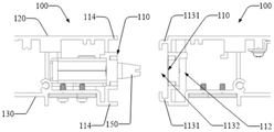
图4是图3中示意出的A部的放大结构示意图。FIG. 4 is an enlarged structural schematic diagram of part A shown in FIG. 3 .
图5是图3中示意出的B部的放大结构示意图。FIG. 5 is an enlarged structural schematic diagram of part B shown in FIG. 3 .
图6是本发明一实施方式的箱体组件的立体结构示意图。Fig. 6 is a schematic perspective view of a box assembly according to an embodiment of the present invention.
图7是图6中示意出的C部的放大结构示意图。FIG. 7 is an enlarged structural schematic diagram of part C shown in FIG. 6 .
图8是图6中示意出的D部的放大结构示意图。FIG. 8 is a schematic diagram of an enlarged structure of part D shown in FIG. 6 .
图9是本发明一实施方式的箱体组件的立体结构示意图。Fig. 9 is a schematic perspective view of a box assembly according to an embodiment of the present invention.
图10是本发明一实施方式的箱体组件的立体结构示意图。Fig. 10 is a schematic perspective view of a box assembly according to an embodiment of the present invention.
图11是本发明一实施方式的箱体组件的主视结构示意图。Fig. 11 is a schematic front view of a box assembly according to an embodiment of the present invention.
图12是本发明一实施方式的箱体组件的部分结构的分解示意图。Fig. 12 is an exploded schematic diagram of a partial structure of a box assembly according to an embodiment of the present invention.
图13是本发明一实施方式的箱体组件的部分结构示意图。Fig. 13 is a partial structural diagram of a box assembly according to an embodiment of the present invention.
附图标记说明如下:The reference signs are explained as follows:
箱体组件10、型材单元100、子型材100a、子型材100b、拼接侧面110、凹槽112、凸部113、凸壁1131、避让空间1132、限位边114、背板120、第二安装位121、第三安装位122、过线结构123、前板130、第一安装位131、容纳空间140、插入件150、磁吸结构170、长度方向L、厚度方向T、宽度方向W。
具体实施方式Detailed ways
尽管本发明可以容易地表现为不同形式的实施方式,但在附图中示出并且在本说明书中将详细说明的仅仅是其中一些具体实施方式,同时可以理解的是本说明书应视为是本发明原理的示范性说明,而并非旨在将本发明限制到在此所说明的那样。While the invention may readily be embodied in different forms, only some of these are shown in the drawings and will be described in detail in this specification, with the understanding that the specification should be considered as the These are exemplary illustrations of the principles of the invention and are not intended to limit the invention to what is described herein.
由此,本说明书中所指出的一个特征将用于说明本发明的一个实施方式的其中一个特征,而不是暗示本发明的每个实施方式必须具有所说明的特征。此外,应当注意的是本说明书描述了许多特征。尽管某些特征可以组合在一起以示出可能的系统设计,但是这些特征也可用于其他的未明确说明的组合。由此,除非另有说明,所说明的组合并非旨在限制。Thus, a feature indicated in this specification will be used to describe one of the features of an embodiment of the present invention, rather than implying that every embodiment of the present invention must have the described feature. Furthermore, it should be noted that this specification describes a number of features. Although certain features may be combined to illustrate possible system designs, these features may also be used in other combinations not explicitly described. Thus, the illustrated combinations are not intended to be limiting unless otherwise stated.
在附图所示的实施方式中,方向的指示(诸如上、下、内、外、左、右、前、后等)用于解释本发明的各种组件的结构和运动不是绝对的而是相对的。当这些组件处于附图所示的位置时,这些说明是合适的。如果这些组件的位置的说明发生改变时,则这些方向的指示也相应地改变。In the embodiments shown in the drawings, directional designations (such as up, down, inside, outside, left, right, front, back, etc.) are used to explain the structure and movement of the various components of the invention are not absolute but rather relatively. These descriptions are applicable when the components are in the positions shown in the drawings. If the description of the location of these components is changed, the indications of these directions are changed accordingly.
现在将参考附图更全面地描述示例实施方式。然而,示例实施方式能够以多种形式实施,且不应被理解为限于在此阐述的范例;相反,提供这些示例实施方式使得本发明的描述将更加全面和完整,并将示例实施方式的构思全面地传达给本领域的技术人员。附图仅为本发明的示意性图解,并非一定是按比例绘制。图中相同的附图标记表示相同或类似的部分,因而将省略对它们的重复描述。Example embodiments will now be described more fully with reference to the accompanying drawings. However, example embodiments may be embodied in many forms and should not be construed as limited to the examples set forth herein; Fully conveyed to those skilled in the art. The drawings are merely schematic illustrations of the invention and are not necessarily drawn to scale. The same reference numerals in the drawings denote the same or similar parts, and thus repeated descriptions thereof will be omitted.
以下结合本说明书的附图,对本发明的较佳实施方式予以进一步地详尽阐述。The preferred implementation modes of the present invention will be further described in detail below in conjunction with the accompanying drawings of this specification.
如图1、图2和图9所示,本发明一个方面的实施例提出了一种箱体组件10,箱体组件10用于显示屏,更详细地,箱体组件10能用于装配显示模组进行显示。As shown in Figure 1, Figure 2 and Figure 9, an embodiment of one aspect of the present invention proposes a
箱体组件10包括两个以上型材单元100,型材单元100之间沿型材单元100的宽度方向W依次排列。举例地,型材单元100为呈长条状的铝型材,型材相较于压铸箱而言在其延伸方向上具有更好的直线精度、相对不易弯折、变形,利于保障箱体组件10在其延伸方向上的直线度,进而利于保障显示模组的装配精度,提高显示效果。The
相邻两个型材单元100的一个设有导向结构,导向结构与另一个型材单元配合使得相邻两个型材单元能拼合在一起,并且相邻两个型材单元在拼合处焊接成一体。One of the two
本发明提供的箱体组件10,在组装过程中通过导向结构对正两个型材单元100,使得型材单元100之间能够保障较高的位置精度,在将对正后的两个型材单元100焊接成一体,一方面,焊接相连的两个型材单元100的整体性更好,避免了型材单元100之间相互松动、错位的风险,进而利于保障显示屏的平度面,另一方面,相邻两个型材单元100在拼合处通过熔焊、电阻焊等处理,使相邻两个型材单元100的材料或者相邻两个型材单元100的材料以及焊料相互渗透融合在一起,这样,以简单的方式实现型材单元100之间可靠、便捷地连接装配,保障型材单元100的装配可靠性,且利于拼接缝的隐藏,使得产品更美观。The
在某些实施例中,至少部分型材单元100的宽度方向W的两端分别形成有拼接侧面110,相邻型材单元100的拼接侧面110相焊接。这样相邻两型材单元100之间的拼接面避开了型材单元100的前侧和背侧,保障拼接可靠的同时,型材单元100的前侧和背侧能具有更好的平整度,实现美化产品的外观以及方便显示模组的安装。In some embodiments, splicing
进一步地,型材单元100的一个拼接侧面110上设有导向结构,型材单元100的导向结构和与之相邻的型材单元100的拼接侧面110相连,使相邻两个型材单元100在型材单元100的厚度方向T上被定位,或者使相邻两个型材单元100在型材单元100的长度方向L上被定位,再或者使相邻两个型材单元100在型材单元100的厚度方向T和长度方向L上均被定位。从而保障相邻两个型材单元100在型材单元100的厚度方向T上的平面度,以及保障相邻两个型材单元100在型材单元100的长度方向L上的整齐度,降低拼接错位的风险性,进而保障显示屏的平面精度,提升显示效果。Further, a
更进一步地,导向结构包括插接部,型材单元100的一个拼接侧面110上设置有插接部,型材单元100的插接部和与之相邻的型材单元100的拼接侧面110相连,使相邻两个型材单元100在型材单元100的厚度方向T和/或长度方向L上被定位。插接的方式实现了相邻两型材单元100之间的隐藏式连接,减少拼接缝的宽度,进一步美化了产品的外观,且插接的方式还具有一定的预固定作用,实现型材单元100之间的初步固定,方便后续的焊接操作。Further, the guide structure includes a splicing portion, and a
在一些具体实施例中,如图10、图11、图12和图13所示,插接部包括插入件150,型材单元100的一个拼接侧面110上设置有多个插入件150,多个插入件150之间沿型材单元100的长度方向L间隔排布。型材单元100的另一个拼接侧面110上形成有多个凹槽112,多个凹槽112和多个插入件150一对一地排布,型材单元100的插入件150插入与之相邻的型材单元100的凹槽112,使相邻两个型材单元100在型材单元100的长度方向L上被定位。这样每个插入件150和与之对应的凹槽112之间位置相对,插入件150插入与之位置相对的凹槽112,使得型材单元100在长度方向L上的两端能够和与之相邻的型材单元100保持平齐,保障相邻两型材单元100在长度方向L上的整齐度。多个插入件150的设计进一步降低相邻两型材单元100在长度方向L上的错位的风险性,产品装配更简单,装配精度更好。In some specific embodiments, as shown in FIG. 10 , FIG. 11 , FIG. 12 and FIG. 13 , the plug-in part includes an
可选地,插入件150设置于拼接侧面110并能够自拼接侧面110上拆卸下来。举例地,插入件150通过紧固件、卡接、胶粘连接、焊接等方式装配于拼接侧面110。这样插入件150能够作为一个独立的部件装配于型材单元100上,简化了型材单元100的结构,降低了加工难度和加工成本。Optionally, the
当然,在其他实施例中也可以设计拼接侧面110的部分区域向外凸起形成插入件150,这样插入件150直接由拼接侧面110加工构造而成,既有利于保障插入件150的位置精度,提升插入件150的定位精准度,又实现了插入件150和拼接侧面110的一体化设计,进一步减少产品的组装步骤。Of course, in other embodiments, it is also possible to design part of the
在另一些具体实施例中,如图3、图4所示,插接部包括凸部113,型材单元100的一个拼接侧面110向外凸起地形成有凸部113,型材单元100的另一个拼接侧面110形成有两个限位边114,两个限位边114在型材单元100的厚度方向T上具有间距,型材单元100的凸部113伸入与之相邻的型材单元100的两个限位边114之间并被两个限位边114所限位,使相邻两个型材单元100在型材单元100的厚度方向T被定位。这样,通过两个限位边114从凸部113的两侧对凸部113止挡限位,使得型材单元100在前后两侧面能够和与之相邻的型材单元100保持平齐,保障相邻两型材单元100在厚度方向T上的平面度,进而保障显示模组的装配平面度,提升显示效果。In some other specific embodiments, as shown in Fig. 3 and Fig. 4, the insertion part includes a
更进一步地,限位边114和凸部113分别沿型材单元100的长度方向L延伸设置,这样限位边114和凸部113分别为沿长度方向L上连续延伸的结构,进一步提升装配精度,在一定程度上使得型材单元100之间的平面度得到纠正和保持。Furthermore, the limiting
当然,以上仅是本发明的一个优选地实施例,在其他实施例中也可以设计限位边114和凸部113为沿长度方向L上间断的结构,或者设计限位边114和凸部113中的一个为沿长度方向L上连续延伸的结构,另一个为沿长度方向L上间断的结构,同样可以使得型材单元100之间的平面度得到纠正和保持。Of course, the above is only a preferred embodiment of the present invention, and in other embodiments, it is also possible to design the limiting
值得说明的是,上述两个具体实施例之间并不冲突,在一些具体实施例中,在同一型材单元100上设有插入件150和凸部113。更佳地,限位边114和插入件150位于型材单元100的同一个拼接侧面110上,凸部113和凹槽112位于型材单元100的另一个拼接侧面110上,这样相邻两个型材单元100相互嵌入对方内部并相连,形成互嵌的结构形式,二相互之间不易错位、松动,定位更精准。It is worth noting that there is no conflict between the above two specific embodiments, and in some specific embodiments, the
更进一步地,凸部113包括两个凸壁1131,两个凸壁1131在型材单元100的厚度方向T上位置相对且具有间距,两个凸壁1131之间限定出避让空间1132,当两个凸壁1131伸入两个限位边114之间,插入部经避让空间1132插入凹槽112内。这样在满足定位的同时,通过避让空间1132使得插入部能更深入地插入凹槽112内,定位更精准。Further, the
可选地,如图6和图7所示,凸壁1131的横截面呈折弯状,提升凸壁1131的强度,避免凸壁1131变形、折断的风险性。并且两个凸壁1131相互朝对方弯折,这样利于增大凸壁1131和限位边114之间的接触面,提升定位的精度。Optionally, as shown in FIG. 6 and FIG. 7 , the cross section of the
在某些实施例中,型材单元100设有第一连接结构,第一连接结构用于与显示模组的第二连接结构相连,以使显示模组装配于型材单元100上,其中,第一连接结构和第二连接结构中的一个为磁吸结构170,另一个为能与磁吸结构170磁吸连接的金属件。相比于现有的显示模组和箱体之间通过两个磁铁相互吸合的方式而言,本实施例通过磁吸结构170和金属件相互吸合的方式,其在保障显示模组和箱体之间连接可靠的同时,适当的减小了吸合力,降低了在装配过程中显示模组由于受到较大的磁吸力而撞碎的风险性。In some embodiments, the
在某些实施例中,如图5和图8所示,每个型材单元100包括至少两个子型材,子型材之间沿型材单元100的宽度方向W并排设置并和与之相邻的子型材焊接成一体。In some embodiments, as shown in FIG. 5 and FIG. 8 , each
具体可以参照图1进行理解,其中,型材单元100包括子型材100a和子型材100b,子型材100a和子型材100b焊接形成一个整体式的型材单元100,两个型材单元100在拼接成箱体组件10。这样子型材之间的排列顺序和型材单元100之间的排列顺序相一致,子型材的长度能够根据显示屏的尺寸需求进行加工、截取,在其长度方向L上无需进行拼装作业,降低拼装错位的风险性,利于保障箱体组件10在长度方向L上的直线度和平面度。Specifically, it can be understood with reference to FIG. 1 , wherein the
并且子型材之间沿横向依次排列并焊接成一体,以实现扩大型材单元100在横向的尺寸,这样利用多个相对较小尺寸的子型材拼合出更大尺寸的型材单元100,针对相同尺寸的显示屏而言,大尺寸的型材单元100实现减少拼装所需的型材单元100的数量,这样既利于减少现场拼装、焊接的物料数量与种类,也利于减少组装步骤,降低装配误差,提升装配精度。And the sub-profiles are arranged in sequence along the transverse direction and welded together to realize the expansion of the size of the
并且,相对小尺寸的子型材相较于大尺寸的子型材而言,加工工艺难度低、加工精度更容易保障,本实施例在实现扩大型材单元100的尺寸的同时,降低子型材的加工难度和加工成本,保障子型材的加工精度,使相对较小尺寸的子型材具有更好的直线精度和平面精度,进一步降低装配误差,提升装配精度。Moreover, compared with large-sized sub-profiles, relatively small-sized sub-profiles are less difficult to process and easier to guarantee machining accuracy. In this embodiment, the processing difficulty of the sub-profiles is reduced while the size of the
举例地,子型材为金属挤压型材,更详细举例地,该子型材为铝挤型材,具有质量轻、强度大、不易变形、成本低的优势,这样经挤压加工一体成型的子型材相对不易变形、弯曲,具有更好的直线度和平面度,进而利于保障显示模组在长度方向L上的装配精度,降低显示模组在长度方向L上错位、凹凸不平的风险性。For example, the sub-profile is a metal extruded profile. For example, in more detail, the sub-profile is an aluminum extruded profile, which has the advantages of light weight, high strength, not easy to deform, and low cost. It is not easily deformed and bent, and has better straightness and flatness, thereby helping to ensure the assembly accuracy of the display module in the length direction L and reducing the risk of dislocation and unevenness of the display module in the length direction L.
在某些实施例中,型材单元100具有位置相对且间隔的背板120和前板130,拼接侧面110衔接背板120和前板130,使背板120、前板130和拼接侧面110共同限定出能用于容纳电控部件的容纳空间140,这样一方面通过拼接侧面110实现背板120和前板130的衔接,且提升了型材单元100的整体强度,降低型材单元100变形、弯折的风险性,另一方面,还能利用容纳空间140装配如电源、接收卡等电控部件,内部布局更紧凑,产品的集成化更高。In some embodiments, the
更详细地,由多个子型材拼接成的型材单元100具有更大的宽幅,进而其容纳空间140更大,内部能够更灵活地布置各类电控部件,尤其是针对小点间距的LED显示屏,更大的容纳空间140有利于降低其内电控部件的密度,各部件间的走线也更方便,且具有很好的散热效果。In more detail, the
进一步地,每个型材单元100的前板130设有多个用于安装显示模组的第一安装位131,每个型材单元100的背板120设有多个用于安装电源的第二安装位121以及多个用于安装接收卡的第三安装位122,其中,第二安装位121的数量和第三安装位122的数量分别小于第一安装位131的数量。这样相较于现有的每个显示模组配置一个电源和接收卡的方案,本实施例优化了显示模组和接收卡以及电源的数量关系,进一步降低其内电控部件的密度,避免电性能会过于冗余的情形,实现节能减材。Further, the
本发明还提供了一种显示屏,包括:两个以上显示模组以及上述任一实施例的箱体组件10,显示模组装配于型材单元100上。The present invention also provides a display screen, comprising: more than two display modules and the
举例地,型材单元100的前板130上设有多个磁吸结构170,显示模组和磁吸结构170磁吸连接以装配于前板130上。For example, the
更进一步地,显示屏为小点间距LED显示屏,其LED点间距在P2.5及以下,如P2.5、P2.083、P1.923、P1.8、P1.667、P1.5、P1.25、P1.0等LED显示屏产品。Furthermore, the display screen is a small dot pitch LED display screen, and its LED dot pitch is P2.5 and below, such as P2.5, P2.083, P1.923, P1.8, P1.667, P1.5, P1.25, P1.0 and other LED display products.
更详细举例地,显示屏为小点间距LED会议屏。In more detail, for example, the display screen is a small dot pitch LED conference screen.
在显示模组供电、信号连接方面,小点间距模组箱体相对大点间距需要更多的连接配合,单位面积上相应端子数量偏多,密度偏大,而本实施例的型材单元100具有更大的宽幅,进而其容纳空间140更大,内部能够更灵活地布置各类电控部件,尤其是针对小点间距的LED显示屏,更大的容纳空间140有利于降低其内电控部件的密度,散热性更好。In terms of power supply and signal connection of the display module, the module cabinet with a small dot pitch requires more connection and coordination than a large dot pitch, and the number of corresponding terminals per unit area is too large, and the density is too high, and the
虽然已参照几个典型实施方式描述了本申请,但应当理解,所用的术语是说明和示例性、而非限制性的术语。由于本申请能够以多种形式具体实施而不脱离发明的精神或实质,所以应当理解,上述实施方式不限于任何前述的细节,而应在随附权利要求所限定的精神和范围内广泛地解释,因此落入权利要求或其等效范围内的全部变化和改型都应为随附权利要求所涵盖。While the present application has been described with reference to several exemplary embodiments, it is understood that the terms which have been used are words of description and illustration, rather than limitation. Since the present application can be embodied in various forms without departing from the spirit or essence of the invention, it should be understood that the above-described embodiments are not limited to any of the foregoing details, but should be construed broadly within the spirit and scope of the appended claims. , all changes and modifications falling within the scope of the claims or their equivalents shall be covered by the appended claims.
Claims (10)
Priority Applications (1)
| Application Number | Priority Date | Filing Date | Title |
|---|---|---|---|
| CN202210999356.5A CN115346451B (en) | 2022-08-19 | 2022-08-19 | Cabinet components and display screen |
Applications Claiming Priority (1)
| Application Number | Priority Date | Filing Date | Title |
|---|---|---|---|
| CN202210999356.5A CN115346451B (en) | 2022-08-19 | 2022-08-19 | Cabinet components and display screen |
Publications (2)
| Publication Number | Publication Date |
|---|---|
| CN115346451A true CN115346451A (en) | 2022-11-15 |
| CN115346451B CN115346451B (en) | 2025-03-28 |
Family
ID=83954318
Family Applications (1)
| Application Number | Title | Priority Date | Filing Date |
|---|---|---|---|
| CN202210999356.5A Active CN115346451B (en) | 2022-08-19 | 2022-08-19 | Cabinet components and display screen |
Country Status (1)
| Country | Link |
|---|---|
| CN (1) | CN115346451B (en) |
Citations (8)
| Publication number | Priority date | Publication date | Assignee | Title |
|---|---|---|---|---|
| KR100682073B1 (en) * | 2006-05-15 | 2007-02-26 | (주)다산에이디 | LED module box assembly for display device |
| CN104050921A (en) * | 2014-06-24 | 2014-09-17 | 西安诺瓦电子科技有限公司 | Display control and monitoring assembly and display system |
| US20190191574A1 (en) * | 2017-12-15 | 2019-06-20 | Lg Display Co., Ltd. | Tiled display device and tiling apparatus therefor |
| CN210767565U (en) * | 2019-08-01 | 2020-06-16 | 李海波 | A cover plate structure of a loft stretched staircase |
| CN111681571A (en) * | 2020-07-27 | 2020-09-18 | 佛山市迪赛曼科技有限公司 | A display screen with integrated design of long strip aluminum profiles and its manufacturing method |
| CN212533783U (en) * | 2020-03-13 | 2021-02-12 | 江苏晟建科技发展有限公司 | Non-metallic sound barrier that can assemble fast |
| CN214169493U (en) * | 2020-10-30 | 2021-09-10 | 陕西能源职业技术学院 | A kind of building sound insulation building board |
| CN218069250U (en) * | 2022-08-19 | 2022-12-16 | 深圳市艾比森光电股份有限公司 | Box body of LED display screen and display screen |
-
2022
- 2022-08-19 CN CN202210999356.5A patent/CN115346451B/en active Active
Patent Citations (8)
| Publication number | Priority date | Publication date | Assignee | Title |
|---|---|---|---|---|
| KR100682073B1 (en) * | 2006-05-15 | 2007-02-26 | (주)다산에이디 | LED module box assembly for display device |
| CN104050921A (en) * | 2014-06-24 | 2014-09-17 | 西安诺瓦电子科技有限公司 | Display control and monitoring assembly and display system |
| US20190191574A1 (en) * | 2017-12-15 | 2019-06-20 | Lg Display Co., Ltd. | Tiled display device and tiling apparatus therefor |
| CN210767565U (en) * | 2019-08-01 | 2020-06-16 | 李海波 | A cover plate structure of a loft stretched staircase |
| CN212533783U (en) * | 2020-03-13 | 2021-02-12 | 江苏晟建科技发展有限公司 | Non-metallic sound barrier that can assemble fast |
| CN111681571A (en) * | 2020-07-27 | 2020-09-18 | 佛山市迪赛曼科技有限公司 | A display screen with integrated design of long strip aluminum profiles and its manufacturing method |
| CN214169493U (en) * | 2020-10-30 | 2021-09-10 | 陕西能源职业技术学院 | A kind of building sound insulation building board |
| CN218069250U (en) * | 2022-08-19 | 2022-12-16 | 深圳市艾比森光电股份有限公司 | Box body of LED display screen and display screen |
Also Published As
| Publication number | Publication date |
|---|---|
| CN115346451B (en) | 2025-03-28 |
Similar Documents
| Publication | Publication Date | Title |
|---|---|---|
| US11470731B1 (en) | Video display panel mounting and aligning system and method | |
| TW201418832A (en) | Curved liquid crystal display device | |
| CN210722258U (en) | Display device | |
| CN210860548U (en) | Reinforcing frame assembly, display main body and spliced intelligent interactive tablet | |
| US11947157B2 (en) | Backlight module and display device | |
| CN212966873U (en) | Corner screen and display screen device | |
| CN101770092A (en) | Liquid crystal display, frame thereof and method for manufacturing frame | |
| US20240346960A1 (en) | Video Display Panel Mounting and Aligning System and Method | |
| EP2081076A2 (en) | Liquid crystal display panel | |
| CN215643496U (en) | display | |
| CN1805673B (en) | Plasma display apparatus | |
| US12075573B2 (en) | Tiling component and tiled display screen | |
| CN215895864U (en) | Box and display device | |
| CN115346451B (en) | Cabinet components and display screen | |
| CN218069250U (en) | Box body of LED display screen and display screen | |
| US20220291766A1 (en) | Infrared touch frame, display device and display apparatus | |
| CN212659246U (en) | Bezel and Display | |
| CN110675768A (en) | LED (light-emitting diode) assembling module | |
| CN106873239A (en) | display device | |
| CN112114692A (en) | Infrared touch frame and display device | |
| CN219876595U (en) | Display screen box, display module and splice display device | |
| CN223743234U (en) | LED cabinets and LED display devices having them | |
| CN219327975U (en) | Quick installation module of LED display module assembly | |
| CN223743233U (en) | LED cabinets and LED display devices having them | |
| JP4008738B2 (en) | Planar light source device and display device |
Legal Events
| Date | Code | Title | Description |
|---|---|---|---|
| PB01 | Publication | ||
| PB01 | Publication | ||
| SE01 | Entry into force of request for substantive examination | ||
| SE01 | Entry into force of request for substantive examination | ||
| GR01 | Patent grant | ||
| GR01 | Patent grant |