CN1126610C - Automated semiconductor processing system - Google Patents
Automated semiconductor processing system Download PDFInfo
- Publication number
- CN1126610C CN1126610C CN99808318A CN99808318A CN1126610C CN 1126610 C CN1126610 C CN 1126610C CN 99808318 A CN99808318 A CN 99808318A CN 99808318 A CN99808318 A CN 99808318A CN 1126610 C CN1126610 C CN 1126610C
- Authority
- CN
- China
- Prior art keywords
- tray
- scale
- magazine
- belt
- wafer
- Prior art date
- Legal status (The legal status is an assumption and is not a legal conclusion. Google has not performed a legal analysis and makes no representation as to the accuracy of the status listed.)
- Expired - Fee Related
Links
Images


Classifications
-
- H—ELECTRICITY
- H01—ELECTRIC ELEMENTS
- H01L—SEMICONDUCTOR DEVICES NOT COVERED BY CLASS H10
- H01L21/00—Processes or apparatus adapted for the manufacture or treatment of semiconductor or solid state devices or of parts thereof
- H01L21/67—Apparatus specially adapted for handling semiconductor or electric solid state devices during manufacture or treatment thereof; Apparatus specially adapted for handling wafers during manufacture or treatment of semiconductor or electric solid state devices or components ; Apparatus not specifically provided for elsewhere
- H01L21/677—Apparatus specially adapted for handling semiconductor or electric solid state devices during manufacture or treatment thereof; Apparatus specially adapted for handling wafers during manufacture or treatment of semiconductor or electric solid state devices or components ; Apparatus not specifically provided for elsewhere for conveying, e.g. between different workstations
- H01L21/67739—Apparatus specially adapted for handling semiconductor or electric solid state devices during manufacture or treatment thereof; Apparatus specially adapted for handling wafers during manufacture or treatment of semiconductor or electric solid state devices or components ; Apparatus not specifically provided for elsewhere for conveying, e.g. between different workstations into and out of processing chamber
- H01L21/67754—Apparatus specially adapted for handling semiconductor or electric solid state devices during manufacture or treatment thereof; Apparatus specially adapted for handling wafers during manufacture or treatment of semiconductor or electric solid state devices or components ; Apparatus not specifically provided for elsewhere for conveying, e.g. between different workstations into and out of processing chamber horizontal transfer of a batch of workpieces
-
- H—ELECTRICITY
- H01—ELECTRIC ELEMENTS
- H01L—SEMICONDUCTOR DEVICES NOT COVERED BY CLASS H10
- H01L21/00—Processes or apparatus adapted for the manufacture or treatment of semiconductor or solid state devices or of parts thereof
- H01L21/67—Apparatus specially adapted for handling semiconductor or electric solid state devices during manufacture or treatment thereof; Apparatus specially adapted for handling wafers during manufacture or treatment of semiconductor or electric solid state devices or components ; Apparatus not specifically provided for elsewhere
- H01L21/677—Apparatus specially adapted for handling semiconductor or electric solid state devices during manufacture or treatment thereof; Apparatus specially adapted for handling wafers during manufacture or treatment of semiconductor or electric solid state devices or components ; Apparatus not specifically provided for elsewhere for conveying, e.g. between different workstations
- H01L21/67739—Apparatus specially adapted for handling semiconductor or electric solid state devices during manufacture or treatment thereof; Apparatus specially adapted for handling wafers during manufacture or treatment of semiconductor or electric solid state devices or components ; Apparatus not specifically provided for elsewhere for conveying, e.g. between different workstations into and out of processing chamber
- H01L21/67742—Mechanical parts of transfer devices
-
- H—ELECTRICITY
- H01—ELECTRIC ELEMENTS
- H01L—SEMICONDUCTOR DEVICES NOT COVERED BY CLASS H10
- H01L21/00—Processes or apparatus adapted for the manufacture or treatment of semiconductor or solid state devices or of parts thereof
- H01L21/67—Apparatus specially adapted for handling semiconductor or electric solid state devices during manufacture or treatment thereof; Apparatus specially adapted for handling wafers during manufacture or treatment of semiconductor or electric solid state devices or components ; Apparatus not specifically provided for elsewhere
- H01L21/677—Apparatus specially adapted for handling semiconductor or electric solid state devices during manufacture or treatment thereof; Apparatus specially adapted for handling wafers during manufacture or treatment of semiconductor or electric solid state devices or components ; Apparatus not specifically provided for elsewhere for conveying, e.g. between different workstations
- H01L21/67763—Apparatus specially adapted for handling semiconductor or electric solid state devices during manufacture or treatment thereof; Apparatus specially adapted for handling wafers during manufacture or treatment of semiconductor or electric solid state devices or components ; Apparatus not specifically provided for elsewhere for conveying, e.g. between different workstations the wafers being stored in a carrier, involving loading and unloading
- H01L21/67769—Storage means
-
- H—ELECTRICITY
- H01—ELECTRIC ELEMENTS
- H01L—SEMICONDUCTOR DEVICES NOT COVERED BY CLASS H10
- H01L21/00—Processes or apparatus adapted for the manufacture or treatment of semiconductor or solid state devices or of parts thereof
- H01L21/67—Apparatus specially adapted for handling semiconductor or electric solid state devices during manufacture or treatment thereof; Apparatus specially adapted for handling wafers during manufacture or treatment of semiconductor or electric solid state devices or components ; Apparatus not specifically provided for elsewhere
- H01L21/677—Apparatus specially adapted for handling semiconductor or electric solid state devices during manufacture or treatment thereof; Apparatus specially adapted for handling wafers during manufacture or treatment of semiconductor or electric solid state devices or components ; Apparatus not specifically provided for elsewhere for conveying, e.g. between different workstations
- H01L21/67763—Apparatus specially adapted for handling semiconductor or electric solid state devices during manufacture or treatment thereof; Apparatus specially adapted for handling wafers during manufacture or treatment of semiconductor or electric solid state devices or components ; Apparatus not specifically provided for elsewhere for conveying, e.g. between different workstations the wafers being stored in a carrier, involving loading and unloading
- H01L21/67772—Apparatus specially adapted for handling semiconductor or electric solid state devices during manufacture or treatment thereof; Apparatus specially adapted for handling wafers during manufacture or treatment of semiconductor or electric solid state devices or components ; Apparatus not specifically provided for elsewhere for conveying, e.g. between different workstations the wafers being stored in a carrier, involving loading and unloading involving removal of lid, door, cover
-
- H—ELECTRICITY
- H01—ELECTRIC ELEMENTS
- H01L—SEMICONDUCTOR DEVICES NOT COVERED BY CLASS H10
- H01L21/00—Processes or apparatus adapted for the manufacture or treatment of semiconductor or solid state devices or of parts thereof
- H01L21/67—Apparatus specially adapted for handling semiconductor or electric solid state devices during manufacture or treatment thereof; Apparatus specially adapted for handling wafers during manufacture or treatment of semiconductor or electric solid state devices or components ; Apparatus not specifically provided for elsewhere
- H01L21/677—Apparatus specially adapted for handling semiconductor or electric solid state devices during manufacture or treatment thereof; Apparatus specially adapted for handling wafers during manufacture or treatment of semiconductor or electric solid state devices or components ; Apparatus not specifically provided for elsewhere for conveying, e.g. between different workstations
- H01L21/67763—Apparatus specially adapted for handling semiconductor or electric solid state devices during manufacture or treatment thereof; Apparatus specially adapted for handling wafers during manufacture or treatment of semiconductor or electric solid state devices or components ; Apparatus not specifically provided for elsewhere for conveying, e.g. between different workstations the wafers being stored in a carrier, involving loading and unloading
- H01L21/67775—Docking arrangements
-
- H—ELECTRICITY
- H01—ELECTRIC ELEMENTS
- H01L—SEMICONDUCTOR DEVICES NOT COVERED BY CLASS H10
- H01L21/00—Processes or apparatus adapted for the manufacture or treatment of semiconductor or solid state devices or of parts thereof
- H01L21/67—Apparatus specially adapted for handling semiconductor or electric solid state devices during manufacture or treatment thereof; Apparatus specially adapted for handling wafers during manufacture or treatment of semiconductor or electric solid state devices or components ; Apparatus not specifically provided for elsewhere
- H01L21/677—Apparatus specially adapted for handling semiconductor or electric solid state devices during manufacture or treatment thereof; Apparatus specially adapted for handling wafers during manufacture or treatment of semiconductor or electric solid state devices or components ; Apparatus not specifically provided for elsewhere for conveying, e.g. between different workstations
- H01L21/67763—Apparatus specially adapted for handling semiconductor or electric solid state devices during manufacture or treatment thereof; Apparatus specially adapted for handling wafers during manufacture or treatment of semiconductor or electric solid state devices or components ; Apparatus not specifically provided for elsewhere for conveying, e.g. between different workstations the wafers being stored in a carrier, involving loading and unloading
- H01L21/67778—Apparatus specially adapted for handling semiconductor or electric solid state devices during manufacture or treatment thereof; Apparatus specially adapted for handling wafers during manufacture or treatment of semiconductor or electric solid state devices or components ; Apparatus not specifically provided for elsewhere for conveying, e.g. between different workstations the wafers being stored in a carrier, involving loading and unloading involving loading and unloading of wafers
- H01L21/67781—Batch transfer of wafers
-
- H—ELECTRICITY
- H01—ELECTRIC ELEMENTS
- H01L—SEMICONDUCTOR DEVICES NOT COVERED BY CLASS H10
- H01L21/00—Processes or apparatus adapted for the manufacture or treatment of semiconductor or solid state devices or of parts thereof
- H01L21/67—Apparatus specially adapted for handling semiconductor or electric solid state devices during manufacture or treatment thereof; Apparatus specially adapted for handling wafers during manufacture or treatment of semiconductor or electric solid state devices or components ; Apparatus not specifically provided for elsewhere
- H01L21/683—Apparatus specially adapted for handling semiconductor or electric solid state devices during manufacture or treatment thereof; Apparatus specially adapted for handling wafers during manufacture or treatment of semiconductor or electric solid state devices or components ; Apparatus not specifically provided for elsewhere for supporting or gripping
- H01L21/687—Apparatus specially adapted for handling semiconductor or electric solid state devices during manufacture or treatment thereof; Apparatus specially adapted for handling wafers during manufacture or treatment of semiconductor or electric solid state devices or components ; Apparatus not specifically provided for elsewhere for supporting or gripping using mechanical means, e.g. chucks, clamps or pinches
- H01L21/68707—Apparatus specially adapted for handling semiconductor or electric solid state devices during manufacture or treatment thereof; Apparatus specially adapted for handling wafers during manufacture or treatment of semiconductor or electric solid state devices or components ; Apparatus not specifically provided for elsewhere for supporting or gripping using mechanical means, e.g. chucks, clamps or pinches the wafers being placed on a robot blade, or gripped by a gripper for conveyance
-
- Y—GENERAL TAGGING OF NEW TECHNOLOGICAL DEVELOPMENTS; GENERAL TAGGING OF CROSS-SECTIONAL TECHNOLOGIES SPANNING OVER SEVERAL SECTIONS OF THE IPC; TECHNICAL SUBJECTS COVERED BY FORMER USPC CROSS-REFERENCE ART COLLECTIONS [XRACs] AND DIGESTS
- Y10—TECHNICAL SUBJECTS COVERED BY FORMER USPC
- Y10S—TECHNICAL SUBJECTS COVERED BY FORMER USPC CROSS-REFERENCE ART COLLECTIONS [XRACs] AND DIGESTS
- Y10S414/00—Material or article handling
- Y10S414/135—Associated with semiconductor wafer handling
- Y10S414/14—Wafer cassette transporting
Abstract
An automated semiconductor processing system has an indexer bay (75) perpendicularly aligned with a process bay (94) within a clean air enclosure (54). An indexer (72) in the indexer bay provides stocking or storage for work in progress semiconductor wafers. Process chambers (68, 70) are located in the process bay. A process robot (66) moves between the indexer bay and process bay to carry semiconductor wafers to and from the process chambers. The process robot has a robot arm (255) vertically moveable along a lift rail (254). Semiconductor wafers are carried offset from the robot arm, to better avoid contamination. The automated system is compact and requires less clean room floor space.
Description
Invention field
Field of the present invention is to be used for process semiconductor wafers, hard disk media, the extremely low automated semiconductor wafer processing process that pollutes the level similar material of Semiconductor substrate and requirement.
Background of invention
Computer, TV, phone and other electronic product comprise a large amount of basic semi-conductor electronic devices.In order to produce electronic product, in very little space, use photoetching technique in Semiconductor substrate, for example make hundreds of semiconductor devices on the semiconductor wafer.Owing to involve minimum geometric scale in making semiconductor devices, the pollutant on semiconductor substrate materials all will produce defective in the final products as dust, dirt, oil stain, metal etc.
For avoiding pollutant, in the clean room, handle Semiconductor substrate.The clean room is the closed area or the space of designing, being equipped with semiconductor manufacturing facility for avoiding polluting.The air of feed-in clean room is through sufficient filtering, to avoid the ambient air contamination clean room.Use pollution that special material and facility keeps the clean room acceptable low-level on.Thereby the construction of clean room and safeguard may be time-consuming and price high.Semiconductor processing equipment in the clean room should be installed as far as possible compactly, and this just need make a large amount of semiconductor wafers handle in a less space, thereby reduces space and reduction expense.Certainly, this also just needs less semiconductor processing equipment, to reduce the requirement to the space, clean room.
The automated semiconductor treatment system that has is sent semi-conducting material with manipulator.These designed manipulators can avoid producing the semi-conductive micronic dust of pollution.Even but through selecting the operation of material and design manipulator meticulously, the motion parts of manipulator still can produce micronic dust.Therefore, need to improve and handle the extremely low technology of polluting the level semiconductor backing material, defective is remained on acceptable level.
Summary of the invention
Aspect invention the 1st, automated semiconductor processing treatment system has a scale cabin or space and one to handle cabin or space in casing.This scale cabin and processor cabin are vertically opposite, constitute the less spatial design of the desired compact in clean room.
Aspect invention the 2nd, a scale is arranged in the scale cabin.This scale mainly is equipped with a plurality of trays, is placed on semiconductor wafer in the magazine with support.Tray carrier in the scale cabin moves tray and magazine, successively from the scale loading position, by a plurality of intermediate storage position, up to the unloading position of scale.By moving and depositing magazine, scale moves continuously by the automated semiconductor treatment system.
Aspect invention the 3rd, the tray carrier comprises an x-axle and y-axle shift system, with vertical and horizontal motion tray in scale.For avoiding the careless tray motion with respect to driving-belt, y axle shift system has a pair of tooth bar to be engaged on the shelf of pallet base.
Aspect invention the 4th, the refraction by prism on the tray is from the right light beam of sensor, detecting on the tray whether magazine is arranged, or in the magazine whether wafer arranged.
Aspect invention the 5th, the arm that the processing machine hand in the automated semiconductor treatment system has an energy to move both vertically along lift rail.This mechanical arm has the forearm section that extends between elbow joint and wrist joint.Chip support lateral run-out elbow joint and wrist joint on mechanical arm.This mechanical arm is compact, but extendible stroke range is arranged.Therefore treatment system only needs less space.
In invention the 6th with separately, one is movably cushioned dividing plate and is placed on the scale top, with the output capacity and the versatility of raising system.
In invention the 7th with separately, novel processing cabin door can better be closed and the encapsulation process cabin.
Aspect invention the 8th, make up two or more functional characteristics discussed above, so that improved automated semiconductor treatment system to be provided.
A target of the present invention provides the automated semiconductor treatment system, makes semiconductor wafer avoid polluting through better designing.
Further object of the present invention provides general, but also is compact automated semiconductor treatment system, to reduce the requirement to the space, clean room.
Other target will be very obvious during functional characteristic and feature performance benefit are narrated in the back.
Brief description of drawings
In all figure, same element marks with same reference number:
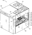
Fig. 1 is automated semiconductor treatment system top, back, left-hand axle side diagrammatic sketch;
Fig. 2 and Fig. 3 are its preceding, top, left-hand axle side diagrammatic sketch;
Fig. 4 is its positive elevation view;
Fig. 5 is its left view;
Fig. 6 is the front perspective view that manipulator shown in Figure 3 advances/goes out;
Fig. 7 is its rear view;
Fig. 8 is the perspective view of scale shown in Fig. 1-3, with the various movable structure parts of clearer expression;
Fig. 9 is the perspective view of other movable structure part of clearer demonstration;
Figure 10 is another perspective view that shows other details;
Figure 11 is the left view of scale shown in Fig. 1-3;
Figure 12 is its plane, with the tray on the clearer expression campaign scale;
Figure 13 is the front view of scale shown in Fig. 1-3;
Figure 14 is the plane of scale shown in Fig. 1-3, with clearer expression sequence of motion;
Figure 15 is the perspective view of elevator shown in Figure 5 when lower position;
Figure 16 is the perspective view of elevator on raised position;
Figure 17 is the front perspective view of Fig. 2 and processing machine hand shown in Figure 5;
Figure 18 is its plane;
Figure 19 is its amplification view;
Figure 20 is the rear view of the arm of processing machine hand when withdrawing fully;
Figure 21 is its plane;
Figure 22 is the side elevation view of processing machine ment face;
Figure 23 is the front perspective view of processing machine hand;
Figure 24 A-24E is the various arm positions of representing the processing machine hand with graphics mode;
Figure 25 is a perspective view of handling the cabin shown in Fig. 3-5;
Figure 26 is Fig. 4, the perspective view in Fig. 5 and semiconductor processes shown in Figure 25 cabin, and have novel door transmission and sealing mechanism;
Figure 27 is a perspective view of handling the cabin door transmission component;
Figure 28 handles the profile of cabin door in the enable possition;
Figure 29 handles the profile of cabin door in the closed position;
Figure 30 is the perspective view of second scale entity apparatus;
Figure 31 is the reverse perspective view of scale shown in Figure 30, with the various movable structure parts of clearer expression.
The detailed description of accompanying drawing
Summary
Accompanying drawing shown in the present further explanatory drawings 1-5, automated semiconductor material handling system 50 is contained in the clean room 52.There are an air cleaning box or chamber 54 in system 50, on its left side wall 56 fixedly transparency window 57 is arranged, thus the working condition in the energy observation ward 54.Equally as shown in Figure 2, there is front wall 58 chamber 54, and it has fixedly transparency window 59.
Uploading in the front wall 58/unload mouthfuls 60 transparently uploaded window or plate 62 is closed by shown in Figure 2 when system's 50 work.Referring to Fig. 1-5,54 tops, chamber are fan or blower fan 80, and it is sent into clean air in the case continuously.Equipment box 82 provides the space of placing power supply, reagent trough, pump and required other parts of semiconductor processes.
Referring to Fig. 1-4, particularly Fig. 3, system 50 comprises a scale cabin or space 75, and it extends back along left side wall 56.Handling cabin or space 94 extends along the front wall perpendicular to scale cabin 75.Scale cabin or space 75 communicate with each other with handling cabin or space 95, and as shown in Figure 3, the interval that separates is just in order to narrate conveniently.Referring to Fig. 1-5, upload/unload window 60 and open scale cabin 75 by the front wall 58 of chamber 54.I/O manipulator 86 in the scale cabin 75 be positioned at window 60 below.
Referring to Fig. 2,3,4, handle cabin 95 and comprise 2 or a plurality of process chamber.More particularly, process chamber is a chemical processing 68 and a centrifugal/flushing drier 70.The processing machine hand moves to scale 72 by handling cabin 95, and wafer 90 is taken out or put into case 68 or 70.
Referring to Fig. 3 and Fig. 5, and Figure 15 and Figure 16, scale 72 following elevators 78 are held out wafer 90 from magazine 88 (uploading two magazines simultaneously), make wafer be picked up and to be transported by processing machine hand 66.As shown in figure 16, each magazine 88 can be adorned 25 wafers, and the ability that scale 72 is held 8 magazines makes it can adorn 200 wafers altogether.With 50 wafers is one group of processing, and elevator 78 and processing machine hand 66 transport the wafer of 2 magazines simultaneously.
The I/O manipulator
Referring to Fig. 6 and Fig. 7, I/O manipulator 86 has an installing plate 110 that connects left plate 56 or adjacent tank body structure.Installing plate 110 is contained on the y axle supporting guide 112.Linear actuator 114 on the guide rail 112 moves the armature 105 of y direction, as Fig. 3 and shown in Figure 6.
Referring to Fig. 7, the x axis rail 106 in armature 105 back is supporting Z axle or vertical inter-digital shape guide rail 102.Vertical inter-digital driver 102 is vertical moving guide rail 102 on armature 105.X through-drive device 108 at x or transversely, with vertical driver 104 mobile vertical guide rails 102.Magazine interdigital 100 tops against vertical guide rail 102 can be inserted magazine side flange 89 and be promoted magazine 88.
Scale
Forward Fig. 8 now to, scale 72 has a rectangular frame 118, and it comprises base plate 120, header board 122, back plate 124, left plate 126 and right plate 128.I/O plate 132 is connected on the right plate 128, is supported by triangular plate 134.Central sill 160 is divided into line of input or input limit 135 and output row 137 to scale.Vertical buffering supports baffle plate 130 to be placed in the buffer board chute 144 of central sill 160 centres, and can seesaw.Two relative tray guide rails 142 extend to right plate 128 from left plate 126, and tray depressed place or surface 139 provide the placement and the supporting surface of tray 136.Referring to Figure 14, scale 72 comprises 10 pallet location: A, B, C, D, E, F, G, H, I and J.Scale 72 has 8 trays 136, so the position at two diagonal angles is always empty.Translate into Figure 12, breaker 162 is arranged in the position C and the H of the base plate 120 of scale 72, can allow air flow downward by scale 72.Elevator mesopore 164 is at I and J place, and it passes base plate 120, and the gap of elevator 78 is provided.
Continuation is referring to Fig. 8-14, and scale 72 comprises x axle or transverse shift system or assembly, is labeled as 140 usually.And y axle or vertical shift system or assembly, be labeled as 170 usually.These shift systems move the tray 136 that is loaded with magazine 88 on scale 72, as shown in figure 14.
Referring to Fig. 9, transverse shift system 140 comprises the transverse guidance piece 150 that is fixed on the scale framework 118.The terminal interdigital 146A of transverse shift is supported on the transverse guidance piece 150, by horizontal drive motor 154 stepping or driving in regular turn between position E and F, as shown in figure 14.Terminal interdigital cylinder 152 is at the terminal interdigital 146A of the rise and fall position lifting of being determined by mechanical stop.Fig. 9 and Figure 10 illustrate the parts of transverse shift system at scale left end or medial extremity.Similar or same parts (transverse guidance piece 150, interdigital 146B and lateral cylinder 152) are installed in right-hand member in the same manner.The transverse shift system connects driving-belt 156 extends around scale framework 118, and it is supported by idle pulley 157, can depend on terminal interdigital 146A in diagonal angle and 146B.When powering up for horizontal drive motor 154, interdigital 146A moves on to position E from position F, and terminal interdigital 146B moves on to position J from position A simultaneously, or carries out in the other direction.
Continuation is referring to Fig. 8-14, scale 72 vertically or y axle shifting part 170 comprise and extend in parallel front and rear panel 122 and 124, or the horizontally-guided rail 172 on central sill 160 arbitrary limits.8 interdigital 180B-180J of side are placed on position B, C, and D, E, G, H, I and J can see too clearly from Figure 12.Interdigital driver of side or cylinder 174 can be attached troops to a unit in 8 sides interdigital 180 any one.Cylinder 174 on horizontal guide rail 172 before and after when motion, can not use interdigital 180 horizontal location of side.8 sides interdigital 180 are linked together by horizontal drive driving-belt 178.Horizontal drive driving-belt 178 stretches along scale framework 118, and is supported by idle pulley.Horizontal drive driving-belt 178 be placed in the scale framework 118 laterally drive driving-belt 156 above.Power up to vertical or y axis drive motor 176, to drive driving-belt 178, its drives the execution of motor 176, makes the interdigital motion simultaneously of all 8 sides.Referring to Figure 12, when motor when the I direction drives the interdigital 180B-180E of side of line of input, the interdigital 180G-180J of side in the central sill 160B opposite output row 137 moves in the O direction.
Referring to Fig. 8-11, scale 72 also comprises bumper bracket shift system or assembly, is labeled as 190 usually.The vertical cushioning fender 130 of these buffering shift system 190 displacements, it supports bumper bracket 76 from anterior locations shown in Figure 9 to back location shown in Figure 8.The bumper bracket 76 that is represented by dotted lines among Fig. 8 is omitted in other figure, to obtain clearer diagrammatic sketch.
Referring to Figure 10, buffering shift system 190 comprises buffering drive motors 198, and it is received buffer by flexible joint 196 and drives driving-belt 200 and driving wheel 192.Buffering drives driving-belt 200 around driving wheel 192 and the buffering driving-belt idle pulley 194 that is positioned at buffering board slot 144 opposites.Vertical cushioning fender 130 can ensure that buffering drives the safety of driving-belt 200.The bottom of vertical cushioning fender 130 can slide into the cushioning fender guide rail 202 below the bumper board slot 144.
Forward Figure 15 and Figure 16 now to, elevator 78 has a motor 210 that links to each other with armature 212, and it transfers Linear Driving to by guiding bolt or other whirligig.The actuating unit of motor 210 promotes armature along the elevator guide rail, and its vertical mobile wafer 90 is sent it into magazine 80, or taken out from magazine.Figure 16 illustrates and take out wafer 90 from magazine 88, and these wafers can be picked up by processing machine hand 66.
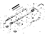
The processing machine hand
Translate into Figure 17-23 now, processing machine hand 66 comprises laterally or x axis rail 250 that it passes processing and handles cabin 95, and some enters scale cabin 75.Transversely guide rail 250 motions of lift unit 252, and driven by magnetic current Linear Driving motor 251.Manipulator arm 255 is connected on the vertical-lift guide rail 254 of lift unit 252.One exchanges lifting motor 257 in vertical direction along lift rail 254 mobile manipulator arms 255.As shown in figure 23, the cylinder 280 of gas spring counting balancer 278 is connected on the manipulator arm 255.Piston 282 is pushed into lift unit 252 to cylinder 280.This gas spring counting balancer applies constant force upwards at manipulator arm 255, promotes motor 257 motion or positioning mechanical arm arm 255 necessary lifting or brake force to reduce.
Continuation is referring to Figure 17-23, and manipulator arm 255 has an elbow to drive alternating current generator 259 in elbow chamber 258.Elbow chamber 258 is against the slideway of lift unit 252 lift rail 254.Forearm 260 is received elbow chamber 258 by arm axle joint 256.Forearm 260 is realized mechanical connection by gear reduction 261 and elbow drive motors 259.
Wrist drives AC servo motor 265 and is contained in the wrist chamber 264, and it receives the outer end of forearm 260 in revolvable mode by wrist joint.Wafer carrier 268 is made of relative bottom clamp 270, it be positioned at wrist chamber 264 under.Groove 274 in the clamp of bottom is used for placing, promotes and carrying wafer 90.Remote control phtographic lens 266 is placed on the top of wrist chamber 264, and is linked to computer 85, is used for observing the chip container position on the manipulator in the processing treatment box, and as United States Patent (USP) 5,784,797 is described.Then, computer just can determine that can processing processing machine hand correctly be inserted into wafer in the treatment box.Phtographic lens 266 is used for also verifying that before the processing of treatment box begins whether fully rotor locking.
Be used to drive wrist drive motors 265, elbow drive motors 259, the amplidyne generator 275 that promotes motor 257 and horizontal drive motor 251 is placed in the lift unit 252, and moves with lift unit.Amplidyne generator is placed on the requirement that has reduced in the lift unit 252 space and cable.
Handle the cabin
Translate into Figure 25 now, that the processing cabin 300 in process chamber 95 comprises is centrifugal/flushing drier 70 and chemical processing 68, though also can use other cabin or increase the cabin in addition.Dividing plate provided final flushing drier 302 before cabin 300 was handled in processing.
Referring to Figure 26-29, handle cabin 300 and comprise a process tank 310, it some in handling alms bowl 314.Process tank 310 matches with movable hatch door 512, and this hatch door can move between the enable possition shown in closed position shown in Figure 26 solid line and the dotted line.
Referring to Figure 26 and 27, hatch door assembly 500 positions are parallel with process tank 310 header boards 502.
Referring to Figure 26 and Figure 27, hatch door gripper shoe 510 is connected on slidably on the leading truck 522.Cylinder 524 is connected on the header board 502 of process tank by installing plate 528.Leading truck 522, cylinder 524 and installing plate 528 provide firm door mounting structure jointly, and do not need other guide rail or back-up block.Leading truck 522 is used to move both vertically, thereby the hatch door assembly can move between the closed position of the enable possition of process tank access material and registration process alms bowl 314 allowing.In the closed position, hatch door can encapsulation process alms bowl 314.
Referring to Figure 28 and 29, the inner sleeve 530 of annular has annular flange 532 and outer cylinder 534.Annular flange 532 is connected on the hatch door gripper shoe 510.A plurality of connectors have guaranteed that outer cylinder ring 516, annular flange 532 are concentric with installing plate 510.
Operation
In use, the operator of system 50 sequence is uploaded in initialization by send into order on user interface 64.Window board 62 is fallen, and uploads window 60 thereby open.The operator is put into the magazine 88 that wafer 90 is housed on the I/O plate 132.When beginning, can be put into magazine 88 on the I/O plate 132 by manually-operated or another manipulator.Lugs 133 location magazines 88 in the I/O plate, thereby can mention by the I/O manipulator, and allow to pass through on the wafer 90 of air in magazine 88.
The interdigital 180B of side among the A of use location below first magazine 88 just makes 8 interdigital air drivers of side or cylinder 174 stretch, and makes side interdigital 180 promote tray, thereby leaves tray depressed place 139.By being in the tray of lifting position, vertical drive motor 176 is with counter-rotation, and interdigital 180B moves on to position B from position A the side that is loaded with first magazine 88 on the tray.After finishing this motion, position A does not just have tray.Because all interdigital drivers 174 of side of control move simultaneously, so the interdigital 180B-J of all sides must move together at the vertical Z direction of principal axis.
Continue to upload or use scale 72 successively, vertical drive motor 176 is retracted position A to the interdigital 180B of side once more, thereby also the interdigital 180J of side is retracted position I from position J.In this motion process, the interdigital cylinder 174 of side descends, thereby does not have the motion of tray.Certainly, interdigital being difficult to of side is positioned at below the tray again.The interdigital end face that will avoid interference in this step motion of side is interdigital, and needs not to be a perfect position.Interdigital 146B has vacateed position J now along with side, and horizontal drive motor 154 moves on to position J to the interdigital 146A of terminal from position A, and simultaneously the interdigital 146A of terminal is moved on to position E from position F.When below the J of position, lateral cylinder 152 extends, and mentions the interdigital 146B of terminal and at the tray of position J, and promotes interdigital 146A simultaneously, with the tray of cocked position E.Horizontal drive motor 154 reverse rotations then (the L direction of Figure 12) are by horizontal driving-belt 156, and interdigital 146A moves on to position F from position E the terminal that is loaded with tray.The lateral cylinder 152 of withdrawing then reduces position A and F that tray enters the scale cabin.
For second tray on the A of position, scale 72 can receive second magazine 88.After second magazine was positioned the I/O plate, I/O manipulator 86 repeated the scale of magazine motion and uploads sequence, thereby can be placed on second magazine on the scale of position A.
Repeat aforesaid step, on magazine uploads to a tray in 8 trays of scale.Because scale has 10 position A-J and 8 trays, thereby position A and the F on diagonal whenever, or position E and J will not have tray.
In scale 72 first and second magazine 88 in-position I and J, the bottom that the elevator 78 that powers up is opened by magazine 88 promotes the wafer platform on lifting post 214 216.Wafer in the magazine is thus lifted to the position of sending into of lifter, and as shown in figure 16, these wafers can be picked up by processing machine hand 66 now.
Referring now to Figure 20,, 21 and 24B, the wafer 90 that processing machine hand 66 takes out in the elevators 78.Laterally drive flow motor 251 horizontal mobile lift units 252, until the wafer carrier 268 correct wafers of aiming on the elevator 78 90.Promote motor 257, elbow drive motors 258 and wrist drive motors 265 by corresponding control, with regard to the mobile wafer carrier 268 of energy, up to arbitrary that is positioned end face manipulation device 270 and alignment wafer, the end face manipulation device has groove 274, can aim at and accept wafer.Shown in Figure 24 B, this wafer handing-over motion is the low hands movement of the arm 255 of manipulator.Wafer carrier 268 moves upward, and takes out wafer 90 from elevator 78.The arm 255 of manipulator is withdrawn into the position shown in Figure 24 C then.Because forearm has 370 ° range of movement, the arm 255 of manipulator can break away from lift unit, returns from scale fully, and only needs minimum gap, shown in Figure 20 and 21.By the motor in the corresponding control manipulator arm, wafer just can keep vertical or subvertical position.
For wafer 90 is delivered to process chamber, horizontal drive motor 251 motion lift units 252 make the selected process chamber of wafer aligned in the wafer carrier 268.The arm 255 of manipulator lifts lift unit by promoting motor 257.In addition, the direction that keeps up by elbow drive motors 257 of forearm 260.The wrist drive motors is driving simultaneously in the other direction, makes wafer carrier be in approximately downward-sloping 10 ° direction, as shown in figure 22.The high hands movement of use shown in Figure 24 A, forearm down stretches, and the wafer carrier that is loaded with wafer is sent into process chamber.The arm 255 of manipulator is withdrawn from process chamber then.
Be cleaning end face manipulation device 270, control wrist drive motors 265 places the vertical direction shown in Figure 24 D to the end face manipulation device.The end face manipulation device is aimed at end face manipulation device flushing drier 302.After to end face manipulation device cleaning and drying, from the withdrawal of end face manipulation device cleaning drier, thereby can transfer wafer, or pick up another group wafer from scale and deliver to process chamber from arbitrary process chamber.Because the end face manipulation device is at process chamber, rather than carries out cleaning in other place, finishing this cleaning does not need the motion process manipulator, thereby can reduce the processing time.
As seen from Figure 23, wafer carrier 268 has an offset distance with the other parts of wrist joint 262 and elbow joint 256 and processing machine hand 66.Processing machine hand 66 directly is positioned at above the wafer without any part.Because the air in the process chamber 54 is to blow over downwards, any micronic dust that processing machine hand 66 produced or emitted can not contact with wafer.Thereby reduced the pollution that wafer may suffer in the processing procedure.
Referring to Figure 24 A-24E, processing machine hand 66 has arm section or the forearm 260 that links to each other with wrist joint 262 with elbow joint 256.Therefore with shoulder, elbow and wrist joint are arranged and the system of two the arm sections that link to each other different, the processing machine hand passes through the motion of arm on lift rail 254 of manipulator, rather than realizes vertical coverage area by the joint of arm segments.This just makes processing machine hand compact conformation, can realize enough range of movement simultaneously.Thereby make very compactness of entire process chamber 54.
Hang down hand and high hands movement because the processing machine hand can be carried out, just define the required vertical stroke of lift rail 254.In addition, carry out low hand and can allow relative short forearm 260, thereby also the process chamber 54 of compactness is made contributions with high chirokinesthetic ability.
Referring to Fig. 1 and Figure 16, when elevator 78 during at upper/lower positions, bumper bracket 76 travels forward (the direction O among Figure 17), to accept 50 wafers.Bumper bracket 76 is arrested wafer, moves on to I and J position up to corresponding empty magazine 88.When bumper bracket 76 was not uploaded or do not uploaded with wafer, it remained in home position (with direction I motion), therefore can not disturb the work of elevator 78.Bumper bracket 76 is temporarily arrested the wafer of having handled, thereby the processing machine hand can take earlier and mobile next group wafer before treated wafer is sent back to scale, and these wafers are sent into process chamber.This has just guaranteed to provide wafer to be processed to process chamber continuously.
Second scale embodiment
Shown in Figure 30 and 31, second scale 600 comprises by side wall 604 and 606, front wall 608, the box 602 that back wall 610 and base plate 612 constitute.Tablet 614 stretches out from front wall 608.Mid-board 616 and horizontal panel 666 are divided into the first row R1 and the second row R2 to scale 600, and there are 5 pallet location or website, A-E just shown in Figure 12 and F-J in each provisional capital.Mid-board is placed in the box 602 by support bar 615, and support bar extends to side wall 604 and 606 from mid-board.
Referring to Figure 30, Buffer Unit 618 comprises the buffering side plate 620 against inside wall 606.Buffering bracket 622 has the comb 624 on comb arm 620.Buffering bracket 622 is supported by buffering bracket post 630.Bracket post 630 can sliding on two buffering guide rails about in the of 632 and 634 on buffering side plate 620.Linear bearing 636 on the bracket post 630 can allow bracket post 630 carry out moving of low-frictional force along guide rail 632 and 634.
Buffering drives drive belt ring around buffering drive motors 638 and terminal pulley 640.Buffering drives driving-belt against the buffering bracket post, thereby the biography that rotatablely moves of motor 638 changes move (the y axle) of buffering bracket post along guide rail 632 and 634 into.As shown in figure 30, the Buffer Unit that is contained on scale 600 side plates is compared with first scale Buffer Unit 72 that is positioned at the center shown in Figure 8, and more compact design is arranged.
Referring to Figure 30 and 31, scale 600 comprise be labeled as usually 650 vertically or y axle displacement assembly, and be labeled as usually 652 laterally or x axle displacement assembly.
Referring to Figure 31, y axle displacement assembly 650 comprises two y axle frameworks 660 side-by-side or in parallel.Each y axle framework 660 comprises the inner side frame frame plate 662 against mid-board 616, and the lateral frame plate 664 on side wall 604 and 606.Laterally 666 of panels are between the inner side frame frame plate 662 and lateral frame plate of y axle framework 660.
Terminal rolling wheel is contained in the end (8 terminal rolling wheels 674 altogether) of internal and external frame plate 662 and 664.Idle pulley 676 is spaced from each other, and is installed on the frame plate 662 and 664 of 674 of terminal rolling wheels.Flat-toothed belt 670 is contained on the terminal rolling wheel 674 and idle pulley 676 of frame plate 662 and 664 (4 flat-toothed belts altogether).Toothed surface on the driving-belt 670 outwardly, so driving-belt contacts with terminal rolling wheel 674 and idle pulley 676 with level and smooth inner face or back.For clearly demonstrating, the part tooth 672 of the driving-belt 670 that only draws, in fact driving-belt 670 has continuous profile of tooth.In addition, do not draw among Figure 31 roller and the driving-belt of front.
Also referring to Figure 31, the y axis drive motor 680 that is contained on the mid-board 616 connects and drive gear set 682, and gear train then drives oppositely and the rotating shaft 684A and the 684B (placed side by side in y axle framework) of constant speed.Drive rotating shaft 684A and 684B and follow driver card wheel 686, drive driving-belt 670 then.The external tooth form face of driving-belt 670 is walked around driver card wheel 686 and idle pulley 688, shown in the dotted line among Figure 31.
As shown in figure 31,10 tray websites determining by horizontal panel 666 or each position among the A-J of position provide the x axle sensor to 690 and the y axle sensor to 696.The x axle sensor is to comprising an infrared transmitter 692 and an Infrared Detectors 694, to each other lateral alignment (on the line perpendicular to frame plate 662 and 664).Equally, the y axle sensor comprises a y axle infrared transmitter 698 and a y axle Infrared Detectors 700 to 696, and they are usually located at the center of horizontal panel 666, and (on the line that is parallel to frame plate 662 and 664) aligned with each other.
On the side wall 604 and 606 of each pallet location A-J, light reflective sensor 702 is arranged, sensor to 690,696 and optical sensor 702 all receive monitor and the controller 85 of control scale 600 work on.
Get back to Figure 30, at the R1 of scale 600 with R2 is capable that 8 rectangle trays 710 are provided, thereby 4 pallet location of each row always take by tray 710, always be sky against the terminal location of end face wall 608 or 610.Each tray all has the tray otch or the opening 712 of rectangle.Shown in Figure 30 dotted line, tray has tray tooth bar 715 on 710 bottom surfaces.Tooth bar 715 extends on the long two sides of tray.The size of tooth bar 715 is consistent with profile of tooth 672 on spacing and the driving-belt.Thereby when tray 712 is placed on the y axle framework 660, the tooth of tray tooth bar 715 just with driving-belt 670 on tooth 672 engagement, so tray pins the y axle motion with respect to driving-belt 670.
Each scale all has a pair of x axle and y axicon.X axle transmitter prism 714 is vertically aimed at the x axle detector prism 716 on each tray 710, as shown in figure 30.Equally, the y axle detector prism 720 on each tray 710 of y axle transmitter prism 718 lateral alignment.On any one position of tray 710 10 pallet location A-J in scale 600, x axle transmitter prism 714 is vertically opposite with x axle detector prism 716, and aims at x axle infrared transmitter 692 and x axle Infrared Detectors 694 in the pallet location respectively.Equally, y axle transmitter prism 718 is vertically opposite with y axle detector prism 720, and aims at y axle infrared transmitter 698 and y axle Infrared Detectors 700 in the pallet location respectively.
Referring to Figure 31, idle pulley 676 has the idle pulley flange 678 that vertically stretches out on driving-belt 670.Idle pulley flange 676 is engaged in the idle pulley groove on each tray 710 bottom surface (shown in the dotted line among Figure 30).Idle pulley flange 678 inserts any x axle motion (unless tray 710 is by vertical-lift) that groove 675 can prevent tray.Therefore tray 710 is supported by driving-belt 710 and idle pulley flange 678.
The operating procedure of scale 600 is similar to the scale of introducing above 72, can be referring to Fig. 8-12.But tray is to realize that by the device control y axis drive motor 680 that computerizeds control it makes the driving-belt incremental motion or increases scale along moving of y axle.Between moving period, tray 710 remains on driving-belt 670 and the idle pulley 676 at the y axle.Different with scale 72, in the scale shown in Figure 30 and 31 600, tray 710 does not move both vertically, the y direction of principal axis motion of tray between pallet location.
In scale 600 end, the x axle motion class of tray 710 is similar to the motion of above-mentioned scale 72, therefore is not described further here.
Whether in each pallet location, whether optical sensor 72 has reverberation by detecting, survey tray 710 and exist.In addition, at each pallet location A-J, whether the x axle sensor is surveyed magazine 88 to 690 and is existed.Particularly use infrared transmitter 692 projecting beam vertically upward.This light beam is by the x axle transmitter prism 714 on each tray 710, and it is 90 ° of light beam foldings, thereby beam level moved in be mapped to x axle detector prism 716.If magazine 88 is arranged on tray 710, light beam will be blocked by magazine 88.On the other hand, if there is not magazine 88 on the tray 710, will be from the infrared light that transmitter 692 sends by x axle transmitter prism 714, by tray 710, downward again by x axle detector prism 716 again, thereby infrared luminous energy arrives and detected by x axle Infrared Detectors 694, illustrates to have magazine 88.
The y axle sensor is used similar approach work to 696, to survey in the magazine 88 whether wafer is arranged.For the magazine on the tray 710 88, the infrared light that y axle transmitter 698 sends throws vertically upward, by y axle transmitter prism half-twist, makes light pass through the slit or the duct 725 of magazine 88 bottoms.If do not have wafer or other planar medium in magazine, light forwards passing hole channel 725 again to downward direction by y axle detector prism 720, and is detected by y axle detector 700, illustrates in magazine 88 without any wafer.If in magazine 88 wafer is arranged, duct 725 will be blocked in the bottom of wafer, makes light can not pass through this duct.Thereby any wafer that exists in the magazine 88 all will block the light that y axle transmitter 698 sends, and y axle detector 700 detects less than light, and just explanation has a wafer at least in magazine 88.
The work of Buffer Unit 618 also is similar to the Buffer Unit 76 shown in top Fig. 8 in the scale 600.But can realize compacter design to the Buffer Unit 618 that is positioned at scale 600 sides.Compare with the scale 72 shown in Fig. 8-16, provide faster and more reliable tray motion with driving-belt 670.Use prism 714-720 to survey magazine and wafer, just do not need to promote tray.
Claims (35)
1. the machine of process semiconductor wafers and plane dielectric material comprises:
A casing;
A scale in the casing, this scale comprises:
One first displacement assembly; With
One second displacement assembly, this second displacement assembly comprises first pair and second pair of driving-belt;
At least attach to the motor of first pair and second pair driving-belt between will having, to drive first pair and second pair of driving-belt in relative direction simultaneously; With
At least can support several trays on the driving-belt.
2. machine according to claim 1, wherein driving-belt is jointless flat-toothed belt, each tray has at least a tooth to be engaged on this jointless flat-toothed belt.
3. machine according to claim 1 and 2, this machine also comprise several separate, rollers of supporting first pair and second pair driving-belt, and these rollers have goes up the flange of lifting these driving-belts, and the flange of roller can partly be supported several trays at least.
4. machine according to claim 1 and 2, wherein each extends to several tray websites continuously to driving-belt, and tray can move on the driving-belt between the scale website, and needn't mention tray from driving-belt.
5. machine according to claim 1, this machine also have a Buffer Unit receiving scale one side.
6. machine according to claim 5, this Buffer Unit also comprise a cushioning fender that leans against on the scale, and a buffering slideway is against this cushioning fender, and a buffer pallet can cushion on the guide rail at this slides.
7. according to the described machine of claim 6, this slideway is parallel to driving-belt.
8. machine according to claim 1 has a pair of prism at least on a tray.
9. machine according to claim 1 also comprises first website in the scale of this machine below first pair of driving-belt, and first pair of sensor arranged in first website, and first pair of prism arranged on a tray at least.
10. machine according to claim 9, this machine also comprises in first website
The tray sensor is used for detecting whether there is tray at first website.
11. machine according to claim 10, this machine also comprises second pair of sensor in first website, second pair of prism arranged on a tray at least, and second pair of prism is facing to the second line, first pair of prism is facing to article one line, and the second line is perpendicular to article one line.
12. machine according to claim 1, this machine also are included in first displacement assembly and recommend out first pair of tray on the driving-belt, drop it off second pair of device on the driving-belt.
13. a processing comprises the machine of planar medium of the wafer of semi-conducting material, comprising:
A scale frame;
In the scale frame, has a flat-toothed belt at least;
Be connected to the motor of at least one flat-toothed belt; With
To the flat-toothed belt of small part support tray, tray has at least a tooth to be engaged on the flat-toothed belt.
14. a processing comprises the machine of planar medium of the wafer of semi-conducting material, comprising:
A scale;
A y axle shift system in this scale;
This y axle shift system is supported several trays;
First pair of prism arranged in a tray at least; With
First pair of sensor with first pair of prism.
15. one kind is the machine that preservation and processing are placed on the planar medium that comprises wafers of semiconductor material in the magazine on the tray, comprising:
First of motion tray shift system on first direction;
At move upward second shift system of tray of the second party perpendicular to first direction;
At least with several tray websites of one of first and second shift system;
Magazine sensor on each tray website;
Planar medium sensor on each tray website;
Magazine sensor prism on each tray is right; With
Planar medium sensor prism on each tray is right.
16. a processing comprises the method for the planar medium of wafers of semiconductor material, comprises the steps:
The magazine that planar medium is housed is put on the tray;
This tray is put into the assigned address on article one driving-belt in the scale;
Calibration article one driving-belt, on the first direction in scale tray from the first tray website incremental motion to the second tray website, and tray continues to remain on article one driving-belt;
From article one driving-belt, vertically mention tray;
Tray along the position that moves to perpendicular to the direction of first direction on the second driving-belt;
Tray is put into assigned address on the second driving-belt; With
Calibration second driving-belt, incremental motion tray on respect to the second direction of first direction, and tray continues to remain on the second driving-belt.
17. an equipment of handling semi-conducting material comprises:
One scale cabin;
Scale in this scale cabin, this scale have a plurality of for keeping the ordinal position of magazine;
Drive system in this scale, be used for the mobile magazine of order and pass through ordinal position, these ordinal positions are configured in two-phase at least and face in the row on limit, and this drive system is included as the first trunnion axis displacement system that vertically moves magazine on scale and for perpendicular to the second trunnion axis mobile system of mobile magazine transversely longitudinally;
The processing cabin in one vertical engagement progress dish cabin;
At least one process chamber in the stow herein; With
The processing machine hand that can move between at least one process chamber therewith at scale.
18. equipment according to claim 17, wherein the equipment of process chamber is placed in centrifugal elutriation drier or the chemical processing.
19. equipment according to claim 17 also comprises one near the end-effector on the manipulator.
20. the equipment of a process semiconductor wafers device comprises:
One has the scale of a plurality of magazine deposit positions;
Magazine reach system in scale is used for order and moves forward magazine by these a plurality of magazine deposit positions;
A plurality of process chambers that the limit is arranged with keeping to the side in an array, this array and scale are perpendicular so that facility compact; With
Be the processing machine hand that moves between scale and process chamber, this manipulator includes:
Be used for the lift rail of vertical portable terminal manipulation device and promote motor;
Be attached to the mechanical arm of lift rail by the elbow joint; With
One wrist joint is attached to this mechanical arm and end-effector is supported to a lift rail and a side that promotes motor, so that manipulator can utilize left-hand seat and following hands movement magazine to be put into and shifted out magazine and process chamber.
21. equipment according to claim 17 also comprises the I/O manipulator that combines with scale, is used for uploading and unload the wafer in the scale.
22. one kind is the equipment of process semiconductor wafers device, comprising:
One has the scale of a plurality of tray deposit positions;
Be used to support the tray of magazine, have the center of opening basically at each tray deposit position;
Tray reach system in the scale, rely on first direction and the second party vertical with first direction move up tray move forward in proper order support magazine tray by a plurality of tray deposit positions in the scale, wherein tray can separate with tray reach system so that tray can move with magazine by scale; With
A plurality of process chambers that the limit is arranged with keeping to the side in an array, this array is vertical with scale so that facility compact.
23. one kind is the method for process semiconductor wafers, comprises step:
One magazine that wafer is housed is sent to the loading website of treatment facility;
In scale in the first row magazine position with first direction increment ground reach magazine, on perpendicular to the second direction of first direction, magazine moved forward into the secondary series magazine position in the scale then;
From magazine, take out wafer;
Wafer is sent into process chamber;
Wafer is inserted process chamber;
In process chamber, handle wafer;
Treated wafer is taken out by process chamber;
Treated wafer is sent back to scale;
Treated wafer is placed on the bumper bracket; With
Take out treated wafer by equipment.
24. method according to claim 23 also is included in the primary importance when taking out wafer, and receives the step of mobile bumper bracket between the second place of treated wafer, in this step treated wafer is put on the bumper bracket.
25. according to claim 23 or 24 described methods, wherein when wafer was mobile between scale and process chamber, the arm of manipulator was held the fixed position of wafer one side.
26. method according to claim 25, wherein the low hand of the arm of manipulator is sent wafer into process chamber, and the master-hand inserts process chamber with wafer.
27. method according to claim 25, wherein the arm of manipulator has an end-effector that is used to hold wafer, it also is included in the step of wafer being inserted cleaning end-effector behind the process chamber, do not need the arm of manipulator is taken out from process chamber, the perpendicular alignmnet end-effector moves down into this end-effector the end-effector cleaner of process chamber then.
28. method according to claim 23 also comprises the step of handling wafer with flushing and centrifugal drying.
29. equipment according to claim 22, wherein tray reach system comprises transverse shift system and the vertical shift system in the scale.
30. equipment according to claim 29, wherein the transverse shift system in scale also is included in a pair of lift elements to the angular direction, promotes actuator and combines with each lift elements, and the transverse shift motor is received each lift elements.
31. equipment according to claim 30, wherein lift elements comprises and is contained in interdigital on the slideway and the lifting actuator that comprises cylinder.
32. equipment according to claim 29, wherein lift elements is received the displacement motor, and is connected with each other by the transverse movement driving-belt.
33. one kind in the automated semiconductor treatment system, operate the method for scale in service, comprise the steps:
First magazine is uploaded to first tray that is arranged in the scale primary importance;
By promoting and transmitting, the primary importance of first tray from scale moved on to the second place; Fall the lift elements below first tray then;
By lift elements to small part before carrying is shifted out below second tray, second tray moved on to primary importance from carrying the front position, to accept second magazine, then second lift elements moved on to below second tray, promote second tray, second tray delivered to primary importance, and then second tray dropped to primary importance; Then
Second magazine is loaded into second tray.
34. method according to claim 33, wherein the translatory movement of second tray is perpendicular to the translatory movement of first tray.
35. method according to claim 33 also is included on the primary importance to detect whether there is a tray at least, the step of wafer in magazine and the magazine.
Applications Claiming Priority (4)
| Application Number | Priority Date | Filing Date | Title |
|---|---|---|---|
| US09/112,259 | 1998-07-08 | ||
| US09/112,259 US6273110B1 (en) | 1997-12-19 | 1998-07-08 | Automated semiconductor processing system |
| US09/274,511 US6279724B1 (en) | 1997-12-19 | 1999-03-23 | Automated semiconductor processing system |
| US09/274,511 | 1999-03-23 |
Publications (2)
| Publication Number | Publication Date |
|---|---|
| CN1308565A CN1308565A (en) | 2001-08-15 |
| CN1126610C true CN1126610C (en) | 2003-11-05 |
Family
ID=26809757
Family Applications (1)
| Application Number | Title | Priority Date | Filing Date |
|---|---|---|---|
| CN99808318A Expired - Fee Related CN1126610C (en) | 1998-07-08 | 1999-06-25 | Automated semiconductor processing system |
Country Status (6)
| Country | Link |
|---|---|
| US (2) | US6279724B1 (en) |
| EP (1) | EP1109632A4 (en) |
| JP (1) | JP2002520140A (en) |
| CN (1) | CN1126610C (en) |
| TW (1) | TW507265B (en) |
| WO (1) | WO2000002675A1 (en) |
Families Citing this family (49)
| Publication number | Priority date | Publication date | Assignee | Title |
|---|---|---|---|---|
| US6471460B1 (en) * | 1996-07-15 | 2002-10-29 | Semitool, Inc. | Apparatus for processing a microelectronic workpiece including a workpiece cassette inventory assembly |
| US6439824B1 (en) | 2000-07-07 | 2002-08-27 | Semitool, Inc. | Automated semiconductor immersion processing system |
| US6736148B2 (en) * | 1997-05-05 | 2004-05-18 | Semitool, Inc. | Automated semiconductor processing system |
| US7067018B2 (en) | 1997-05-05 | 2006-06-27 | Semitool, Inc. | Automated system for handling and processing wafers within a carrier |
| US20030051972A1 (en) * | 1997-05-05 | 2003-03-20 | Semitool, Inc. | Automated immersion processing system |
| US20030051974A1 (en) * | 1997-05-05 | 2003-03-20 | Semitool, Inc. | Automated semiconductor processing system |
| US6572320B2 (en) * | 1997-05-05 | 2003-06-03 | Semitool, Inc. | Robot for handling workpieces in an automated processing system |
| US6454514B2 (en) | 1998-07-08 | 2002-09-24 | Semitool, Inc. | Microelectronic workpiece support and apparatus using the support |
| JP3513437B2 (en) * | 1999-09-01 | 2004-03-31 | キヤノン株式会社 | Substrate management method and semiconductor exposure apparatus |
| US6502054B1 (en) | 1999-11-22 | 2002-12-31 | Lam Research Corporation | Method of and apparatus for dynamic alignment of substrates |
| US6629053B1 (en) * | 1999-11-22 | 2003-09-30 | Lam Research Corporation | Method and apparatus for determining substrate offset using optimization techniques |
| JP2001291698A (en) * | 2000-04-10 | 2001-10-19 | Nec Corp | Apparatus for treatment and method therefor |
| CH714282B1 (en) * | 2000-07-06 | 2019-04-30 | Murata Machinery Ltd | Storage system with conveyor elements. |
| AU2001268656A1 (en) * | 2000-07-07 | 2002-01-21 | Semitool, Inc. | Automated processing system |
| US20040025901A1 (en) * | 2001-07-16 | 2004-02-12 | Semitool, Inc. | Stationary wafer spin/spray processor |
| US6668844B2 (en) | 2001-07-16 | 2003-12-30 | Semitool, Inc. | Systems and methods for processing workpieces |
| WO2003008114A1 (en) * | 2001-07-16 | 2003-01-30 | Semitool, Inc. | Systems and methods for processing workpieces |
| JP2005510055A (en) | 2001-11-13 | 2005-04-14 | エフエスアイ インターナショナル インコーポレイテッド | Reduced footprint tool for automated processing of microelectronic substrates |
| EP1460676A3 (en) * | 2001-11-13 | 2005-10-26 | FSI International, Inc. | Reduced footprint tool for automated processing of microelectronic substrates |
| GB0204882D0 (en) * | 2002-03-01 | 2002-04-17 | Trikon Technologies Ltd | Pedestal |
| JP4033689B2 (en) * | 2002-03-01 | 2008-01-16 | 東京エレクトロン株式会社 | Liquid processing apparatus and liquid processing method |
| US6893505B2 (en) | 2002-05-08 | 2005-05-17 | Semitool, Inc. | Apparatus and method for regulating fluid flows, such as flows of electrochemical processing fluids |
| US6830057B2 (en) * | 2002-11-01 | 2004-12-14 | Semitool, Inc. | Wafer container cleaning system |
| US7289734B2 (en) * | 2002-12-24 | 2007-10-30 | Tropic Networks Inc. | Method and system for multi-level power management in an optical network |
| JP4606195B2 (en) | 2004-03-08 | 2011-01-05 | 富士フイルム株式会社 | Liquid crystal compound, liquid crystal composition, polymer, retardation plate, and elliptically polarizing plate |
| US7905960B2 (en) | 2004-03-24 | 2011-03-15 | Jusung Engineering Co., Ltd. | Apparatus for manufacturing substrate |
| US7783383B2 (en) * | 2004-12-22 | 2010-08-24 | Intelligent Hospital Systems Ltd. | Automated pharmacy admixture system (APAS) |
| EP1830782B1 (en) * | 2004-12-22 | 2013-06-05 | Intelligent Hospital Systems Ltd. | Automated pharmacy admixture system (APAS) |
| JP4613079B2 (en) | 2005-03-04 | 2011-01-12 | 富士フイルム株式会社 | Liquid crystal composition, retardation plate and elliptically polarizing plate |
| DE102005017945A1 (en) * | 2005-04-18 | 2006-10-19 | Paul Hartmann Ag | First aid kit to be stored in vehicle, comprising plastic cover with vacuum created inside for size reduction |
| US8821099B2 (en) | 2005-07-11 | 2014-09-02 | Brooks Automation, Inc. | Load port module |
| US7931859B2 (en) | 2005-12-22 | 2011-04-26 | Intelligent Hospital Systems Ltd. | Ultraviolet sanitization in pharmacy environments |
| ITBO20060559A1 (en) * | 2006-07-26 | 2008-01-27 | Tissue Logistics Solutions S P A | MACHINE FOR THE PRODUCTION OF GROUPS OF ROLLED PRODUCTS. |
| US9117859B2 (en) | 2006-08-31 | 2015-08-25 | Brooks Automation, Inc. | Compact processing apparatus |
| US7602562B2 (en) | 2007-05-21 | 2009-10-13 | Electro Scientific Industries, Inc. | Fluid counterbalance for a laser lens used to scribe an electronic component substrate |
| US8271138B2 (en) | 2007-09-12 | 2012-09-18 | Intelligent Hospital Systems Ltd. | Gripper device |
| US8225824B2 (en) | 2007-11-16 | 2012-07-24 | Intelligent Hospital Systems, Ltd. | Method and apparatus for automated fluid transfer operations |
| JP4515507B2 (en) * | 2008-01-31 | 2010-08-04 | 東京エレクトロン株式会社 | Plasma processing system |
| DE102008027861A1 (en) * | 2008-06-11 | 2009-12-17 | Vistec Semiconductor Systems Jena Gmbh | Device for holding disc-shaped objects |
| US10294658B2 (en) | 2008-12-23 | 2019-05-21 | Xoma (Us) Llc | Flexible manufacturing system |
| US8386070B2 (en) | 2009-03-18 | 2013-02-26 | Intelligent Hospital Systems, Ltd | Automated pharmacy admixture system |
| US8626329B2 (en) * | 2009-11-20 | 2014-01-07 | Agr Automation Ltd. | Product assembly system and control software |
| JP5614352B2 (en) * | 2011-03-29 | 2014-10-29 | 東京エレクトロン株式会社 | Loading unit and processing system |
| KR101363479B1 (en) | 2012-04-20 | 2014-02-17 | 주식회사 엘지화학 | Polymerizable liquid crystal compounds, polymerizable liquid crystal composition, and optically anisotropic body |
| CN102921677B (en) * | 2012-10-24 | 2015-06-03 | 深圳创维-Rgb电子有限公司 | Automatic brushing and decontaminating integrated machine for power supply boards |
| CN104813438B (en) | 2012-11-28 | 2017-07-25 | 盛美半导体设备(上海)有限公司 | The cleaning method and device of semi-conductor silicon chip |
| AT515531B1 (en) * | 2014-09-19 | 2015-10-15 | Siconnex Customized Solutions Gmbh | Mounting system and feeding method for disc-shaped objects |
| KR101734241B1 (en) * | 2015-12-10 | 2017-05-11 | 현대자동차 주식회사 | Trunk lid hinge intellectual loader unit |
| TWI674930B (en) * | 2017-04-18 | 2019-10-21 | 韓商Sti股份有限公司 | Apparatus for cleaning container |
Family Cites Families (33)
| Publication number | Priority date | Publication date | Assignee | Title |
|---|---|---|---|---|
| NL176841C (en) * | 1975-03-04 | 1985-06-17 | Philips Nv | TRANSPORTATION DEVICE FOR TEST SAMPLE CARRERS, AND THESE CARRIERS. |
| FR2314390A1 (en) * | 1975-06-13 | 1977-01-07 | Sofermo | AUTONOMOUS MODULAR JOINT FOR VARIOUS MECHANISMS AND IN PARTICULAR FOR ROBOTS |
| US4506777A (en) * | 1978-12-04 | 1985-03-26 | Beckman Instruments, Inc. | Sample handling apparatus |
| DE3171220D1 (en) | 1980-09-02 | 1985-08-08 | Heraeus Schott Quarzschmelze | Method of and apparatus for transferring semiconductor wafers between carrier members |
| DE3114032C2 (en) * | 1981-04-07 | 1983-04-14 | Gerd 8151 Osterwarngau Stückler | Parts feed for an assembly table |
| JPS59114206A (en) * | 1982-12-21 | 1984-07-02 | Toshiba Corp | Pallet conveyor device |
| US4568234A (en) | 1983-05-23 | 1986-02-04 | Asq Boats, Inc. | Wafer transfer apparatus |
| US4667081A (en) * | 1985-02-04 | 1987-05-19 | Spectra-Physics, Inc. | Apparatus for changing the direction of a light beam passing through an articulated joint |
| US4806057A (en) * | 1986-04-22 | 1989-02-21 | Motion Manufacturing, Inc. | Automatic wafer loading method and apparatus |
| JPS63219134A (en) | 1987-03-09 | 1988-09-12 | Mitsubishi Electric Corp | Wafer handling device of diffusion furnace |
| US5030057A (en) * | 1987-11-06 | 1991-07-09 | Tel Sagami Limited | Semiconductor wafer transferring method and apparatus and boat for thermal treatment of a semiconductor wafer |
| US5431421A (en) | 1988-05-25 | 1995-07-11 | Semitool, Inc. | Semiconductor processor wafer holder |
| US5064337A (en) | 1988-07-19 | 1991-11-12 | Tokyo Electron Limited | Handling apparatus for transferring carriers and a method of transferring carriers |
| JPH02286510A (en) * | 1989-04-28 | 1990-11-26 | Tsubakimoto Chain Co | Bogie connection type conveyor |
| US5203445A (en) * | 1990-03-17 | 1993-04-20 | Tokyo Electron Sagami Limited | Carrier conveying apparatus |
| US5186594A (en) | 1990-04-19 | 1993-02-16 | Applied Materials, Inc. | Dual cassette load lock |
| JPH081922B2 (en) * | 1991-01-25 | 1996-01-10 | 株式会社東芝 | Wafer-holding device |
| US5232328A (en) | 1991-03-05 | 1993-08-03 | Semitool, Inc. | Robot loadable centrifugal semiconductor processor with extendible rotor |
| JPH081923B2 (en) | 1991-06-24 | 1996-01-10 | ティーディーケイ株式会社 | Clean transfer method and device |
| JPH05146984A (en) | 1991-07-08 | 1993-06-15 | Murata Mach Ltd | Robot for handling wafer cassette |
| US5215420A (en) | 1991-09-20 | 1993-06-01 | Intevac, Inc. | Substrate handling and processing system |
| NL9200446A (en) | 1992-03-10 | 1993-10-01 | Tempress B V | Apparatus for handling microcircuit disks (wafers). |
| US5378145A (en) | 1992-07-15 | 1995-01-03 | Tokyo Electron Kabushiki Kaisha | Treatment system and treatment apparatus |
| DE4404902C2 (en) * | 1994-02-16 | 2002-04-11 | Hauni Maschinenbau Ag | Method and device for handling containers holding cigarette trays |
| US5544421A (en) * | 1994-04-28 | 1996-08-13 | Semitool, Inc. | Semiconductor wafer processing system |
| US5784797A (en) | 1994-04-28 | 1998-07-28 | Semitool, Inc. | Carrierless centrifugal semiconductor processing system |
| US5664337A (en) | 1996-03-26 | 1997-09-09 | Semitool, Inc. | Automated semiconductor processing systems |
| ATE275759T1 (en) | 1995-03-28 | 2004-09-15 | Brooks Automation Gmbh | LOADING AND UNLOADING STATION FOR SEMICONDUCTOR PROCESSING SYSTEMS |
| US5613821A (en) | 1995-07-06 | 1997-03-25 | Brooks Automation, Inc. | Cluster tool batchloader of substrate carrier |
| US5674039A (en) | 1996-07-12 | 1997-10-07 | Fusion Systems Corporation | System for transferring articles between controlled environments |
| US5731678A (en) | 1996-07-15 | 1998-03-24 | Semitool, Inc. | Processing head for semiconductor processing machines |
| CH697146A5 (en) * | 1996-10-09 | 2008-05-15 | Tec Sem Ag | Gripping device for handling wafers. |
| US5885045A (en) * | 1997-03-17 | 1999-03-23 | Fortrend Engineering Corporation | Integrated wafer pod-load/unload and mass-transfer system |
-
1999
- 1999-03-23 US US09/274,511 patent/US6279724B1/en not_active Expired - Lifetime
- 1999-06-25 JP JP2000558925A patent/JP2002520140A/en active Pending
- 1999-06-25 EP EP99930722A patent/EP1109632A4/en not_active Withdrawn
- 1999-06-25 WO PCT/US1999/014414 patent/WO2000002675A1/en not_active Application Discontinuation
- 1999-06-25 CN CN99808318A patent/CN1126610C/en not_active Expired - Fee Related
- 1999-07-01 TW TW088111176A patent/TW507265B/en not_active IP Right Cessation
-
2001
- 2001-08-17 US US09/932,719 patent/US20020044855A1/en not_active Abandoned
Also Published As
| Publication number | Publication date |
|---|---|
| JP2002520140A (en) | 2002-07-09 |
| CN1308565A (en) | 2001-08-15 |
| EP1109632A4 (en) | 2006-11-22 |
| WO2000002675A9 (en) | 2000-07-06 |
| US20020044855A1 (en) | 2002-04-18 |
| EP1109632A1 (en) | 2001-06-27 |
| US6279724B1 (en) | 2001-08-28 |
| WO2000002675A1 (en) | 2000-01-20 |
| TW507265B (en) | 2002-10-21 |
Similar Documents
| Publication | Publication Date | Title |
|---|---|---|
| CN1126610C (en) | Automated semiconductor processing system | |
| JP7432457B2 (en) | Substrate processing system | |
| CN1269707C (en) | Modular sorter | |
| US7311488B2 (en) | System and method for conveying flat panel display | |
| CN1118428C (en) | Integrated load port-conveyor transfer system | |
| CN1294658C (en) | Universal tool interface and/or workpiece transfer apparatus for SMIF and open pod applications | |
| CN102122609B (en) | The multidirectional inline processing apparatus of auto-sequencing | |
| TWI430932B (en) | The workpiece is moved into the system and the handling device | |
| US10403528B2 (en) | Substrate-processing apparatus and method of manufacturing semiconductor device | |
| CN1574271A (en) | Substrate conveying device and conveying method, and vacuum disposal device | |
| CN111964591B (en) | Electronic product part detection system | |
| US20030159277A1 (en) | Method and apparatus for manually and automatically processing microelectronic workpieces | |
| CN213004545U (en) | Sweep light device and sweep ray apparatus | |
| CN1728356A (en) | Substrate processor | |
| JP2003218018A (en) | Processing device | |
| JP2020164282A (en) | Panel transfer system | |
| CN1689140A (en) | Method and apparatus for supplying substrates to a processing tool | |
| CN1707272A (en) | Inspection apparatus | |
| JP2515879Y2 (en) | Substrate support | |
| JP2511728B2 (en) | Substrate feeding / discharging device | |
| JP5872880B2 (en) | Substrate processing apparatus, substrate transfer apparatus, and semiconductor device manufacturing method | |
| JP4237017B2 (en) | Substrate transfer device | |
| JPH06275700A (en) | Board processing system and carrier conveyor | |
| CN113927451A (en) | Light scanning machine and light scanning control method | |
| JPH05109867A (en) | Mechanical interface device |
Legal Events
| Date | Code | Title | Description |
|---|---|---|---|
| C06 | Publication | ||
| PB01 | Publication | ||
| C10 | Entry into substantive examination | ||
| SE01 | Entry into force of request for substantive examination | ||
| C14 | Grant of patent or utility model | ||
| GR01 | Patent grant | ||
| C19 | Lapse of patent right due to non-payment of the annual fee | ||
| CF01 | Termination of patent right due to non-payment of annual fee |