CN112579043A - Compute/near memory Compute (CIM) circuit architecture in memory - Google Patents
Compute/near memory Compute (CIM) circuit architecture in memory Download PDFInfo
- Publication number
- CN112579043A CN112579043A CN202010578598.8A CN202010578598A CN112579043A CN 112579043 A CN112579043 A CN 112579043A CN 202010578598 A CN202010578598 A CN 202010578598A CN 112579043 A CN112579043 A CN 112579043A
- Authority
- CN
- China
- Prior art keywords
- memory
- mac
- array
- cnm
- mux
- Prior art date
- Legal status (The legal status is an assumption and is not a legal conclusion. Google has not performed a legal analysis and makes no representation as to the accuracy of the status listed.)
- Pending
Links
Images

Classifications
-
- G—PHYSICS
- G06—COMPUTING OR CALCULATING; COUNTING
- G06F—ELECTRIC DIGITAL DATA PROCESSING
- G06F7/00—Methods or arrangements for processing data by operating upon the order or content of the data handled
- G06F7/38—Methods or arrangements for performing computations using exclusively denominational number representation, e.g. using binary, ternary, decimal representation
- G06F7/48—Methods or arrangements for performing computations using exclusively denominational number representation, e.g. using binary, ternary, decimal representation using non-contact-making devices, e.g. tube, solid state device; using unspecified devices
- G06F7/544—Methods or arrangements for performing computations using exclusively denominational number representation, e.g. using binary, ternary, decimal representation using non-contact-making devices, e.g. tube, solid state device; using unspecified devices for evaluating functions by calculation
- G06F7/5443—Sum of products
-
- G—PHYSICS
- G06—COMPUTING OR CALCULATING; COUNTING
- G06F—ELECTRIC DIGITAL DATA PROCESSING
- G06F12/00—Accessing, addressing or allocating within memory systems or architectures
- G06F12/02—Addressing or allocation; Relocation
- G06F12/0223—User address space allocation, e.g. contiguous or non contiguous base addressing
- G06F12/023—Free address space management
- G06F12/0238—Memory management in non-volatile memory, e.g. resistive RAM or ferroelectric memory
- G06F12/0246—Memory management in non-volatile memory, e.g. resistive RAM or ferroelectric memory in block erasable memory, e.g. flash memory
-
- G—PHYSICS
- G06—COMPUTING OR CALCULATING; COUNTING
- G06F—ELECTRIC DIGITAL DATA PROCESSING
- G06F12/00—Accessing, addressing or allocating within memory systems or architectures
- G06F12/02—Addressing or allocation; Relocation
- G06F12/08—Addressing or allocation; Relocation in hierarchically structured memory systems, e.g. virtual memory systems
- G06F12/0802—Addressing of a memory level in which the access to the desired data or data block requires associative addressing means, e.g. caches
- G06F12/0806—Multiuser, multiprocessor or multiprocessing cache systems
- G06F12/0811—Multiuser, multiprocessor or multiprocessing cache systems with multilevel cache hierarchies
-
- G—PHYSICS
- G06—COMPUTING OR CALCULATING; COUNTING
- G06F—ELECTRIC DIGITAL DATA PROCESSING
- G06F12/00—Accessing, addressing or allocating within memory systems or architectures
- G06F12/02—Addressing or allocation; Relocation
- G06F12/08—Addressing or allocation; Relocation in hierarchically structured memory systems, e.g. virtual memory systems
- G06F12/0802—Addressing of a memory level in which the access to the desired data or data block requires associative addressing means, e.g. caches
- G06F12/0875—Addressing of a memory level in which the access to the desired data or data block requires associative addressing means, e.g. caches with dedicated cache, e.g. instruction or stack
-
- G—PHYSICS
- G06—COMPUTING OR CALCULATING; COUNTING
- G06F—ELECTRIC DIGITAL DATA PROCESSING
- G06F15/00—Digital computers in general; Data processing equipment in general
- G06F15/76—Architectures of general purpose stored program computers
- G06F15/78—Architectures of general purpose stored program computers comprising a single central processing unit
- G06F15/7807—System on chip, i.e. computer system on a single chip; System in package, i.e. computer system on one or more chips in a single package
- G06F15/7825—Globally asynchronous, locally synchronous, e.g. network on chip
-
- G—PHYSICS
- G06—COMPUTING OR CALCULATING; COUNTING
- G06F—ELECTRIC DIGITAL DATA PROCESSING
- G06F17/00—Digital computing or data processing equipment or methods, specially adapted for specific functions
- G06F17/10—Complex mathematical operations
- G06F17/16—Matrix or vector computation, e.g. matrix-matrix or matrix-vector multiplication, matrix factorization
-
- G—PHYSICS
- G06—COMPUTING OR CALCULATING; COUNTING
- G06F—ELECTRIC DIGITAL DATA PROCESSING
- G06F7/00—Methods or arrangements for processing data by operating upon the order or content of the data handled
- G06F7/38—Methods or arrangements for performing computations using exclusively denominational number representation, e.g. using binary, ternary, decimal representation
- G06F7/48—Methods or arrangements for performing computations using exclusively denominational number representation, e.g. using binary, ternary, decimal representation using non-contact-making devices, e.g. tube, solid state device; using unspecified devices
- G06F7/491—Computations with decimal numbers radix 12 or 20.
- G06F7/498—Computations with decimal numbers radix 12 or 20. using counter-type accumulators
- G06F7/4981—Adding; Subtracting
-
- G—PHYSICS
- G06—COMPUTING OR CALCULATING; COUNTING
- G06F—ELECTRIC DIGITAL DATA PROCESSING
- G06F7/00—Methods or arrangements for processing data by operating upon the order or content of the data handled
- G06F7/38—Methods or arrangements for performing computations using exclusively denominational number representation, e.g. using binary, ternary, decimal representation
- G06F7/48—Methods or arrangements for performing computations using exclusively denominational number representation, e.g. using binary, ternary, decimal representation using non-contact-making devices, e.g. tube, solid state device; using unspecified devices
- G06F7/491—Computations with decimal numbers radix 12 or 20.
- G06F7/498—Computations with decimal numbers radix 12 or 20. using counter-type accumulators
- G06F7/4983—Multiplying; Dividing
-
- G—PHYSICS
- G06—COMPUTING OR CALCULATING; COUNTING
- G06F—ELECTRIC DIGITAL DATA PROCESSING
- G06F9/00—Arrangements for program control, e.g. control units
- G06F9/06—Arrangements for program control, e.g. control units using stored programs, i.e. using an internal store of processing equipment to receive or retain programs
- G06F9/30—Arrangements for executing machine instructions, e.g. instruction decode
- G06F9/30098—Register arrangements
-
- G—PHYSICS
- G06—COMPUTING OR CALCULATING; COUNTING
- G06F—ELECTRIC DIGITAL DATA PROCESSING
- G06F2207/00—Indexing scheme relating to methods or arrangements for processing data by operating upon the order or content of the data handled
- G06F2207/38—Indexing scheme relating to groups G06F7/38 - G06F7/575
- G06F2207/48—Indexing scheme relating to groups G06F7/48 - G06F7/575
- G06F2207/4802—Special implementations
- G06F2207/4818—Threshold devices
- G06F2207/4824—Neural networks
-
- G—PHYSICS
- G06—COMPUTING OR CALCULATING; COUNTING
- G06F—ELECTRIC DIGITAL DATA PROCESSING
- G06F2212/00—Indexing scheme relating to accessing, addressing or allocation within memory systems or architectures
- G06F2212/10—Providing a specific technical effect
- G06F2212/1016—Performance improvement
-
- G—PHYSICS
- G06—COMPUTING OR CALCULATING; COUNTING
- G06F—ELECTRIC DIGITAL DATA PROCESSING
- G06F2212/00—Indexing scheme relating to accessing, addressing or allocation within memory systems or architectures
- G06F2212/45—Caching of specific data in cache memory
- G06F2212/454—Vector or matrix data
Landscapes
- Engineering & Computer Science (AREA)
- Physics & Mathematics (AREA)
- Theoretical Computer Science (AREA)
- General Physics & Mathematics (AREA)
- General Engineering & Computer Science (AREA)
- Computing Systems (AREA)
- Pure & Applied Mathematics (AREA)
- Mathematical Optimization (AREA)
- Mathematical Analysis (AREA)
- Computational Mathematics (AREA)
- Mathematical Physics (AREA)
- Data Mining & Analysis (AREA)
- Software Systems (AREA)
- Algebra (AREA)
- Databases & Information Systems (AREA)
- Computer Hardware Design (AREA)
- Microelectronics & Electronic Packaging (AREA)
- Logic Circuits (AREA)
Abstract
A memory circuit includes a plurality (X) of multiply-accumulate (MAC) circuits that are dynamically configurable. The MAC circuit may compute the output based on the computation of X elements of the input vector and the weight vector, or based on the computation of a single element of the input vector and the weight vector, where each element has a length of one or more bits. The first memory may hold input vectors having a width of X elements, while the second memory may store weight vectors. The MAC circuit includes an on-chip MAC array having a first memory.
Description
Technical Field
The description relates generally to in-memory computation/near-memory Computation (CIM), and more particularly to dynamically switching between matrix-matrix computation and matrix-vector computation with common CIM hardware.
Background
Computer Artificial Intelligence (AI) has been built on machine learning, particularly using deep learning techniques. Through deep learning, computing systems organized as neural networks compute statistical likelihoods of input data matching existing computed data. Neural networks involve a plurality of interconnected processing nodes that enable data analysis to compare inputs to "trained" data. Trained data involves computational analysis of the properties of known data to develop models for comparing input data.
Certain deep learning applications, such as those that apply single or small batches of MLP (multi-layer perceptron), RNN (recurrent neural network), and LSTM (long-short term memory — recurrent neural network with feedback), typically perform matrix-vector (MxV) multiplication, in which a vector of neuron activations (or narrow matrix) is multiplied by a neural network weight matrix.
Other deep learning applications, such as those that apply CNN (convolutional neural networks, such as for image processing, video processing, or computation or classification of two-dimensional (2D) images) or large batches of MLP, are typically mapped to matrix-matrix (MxM) multiplication, where the matrix is multiplied by a neural network weight matrix.
The dot product operation for both MxV and MxM is performed by using an array of multiply-accumulate (MAC) arithmetic units. A two-dimensional (2D) systolic array (systolic array) of MAC units can provide a hardware solution for MxM operations with good performance and data reuse. The one-dimensional (1D) computational array approach is more suitable than the 2D systolic array to maximize data reuse of vector elements. Thus, the 1D computational array provides good performance for the MxV operation. Thus, MxV multiplications generally map well to 1D computational arrays, whereas MxM multiplications generally map well to 2D computational arrays.
However, performing MxV on the 2D systolic array drastically drops the ratio of computation to memory Bandwidth (BW). Similarly, executing MxM on a 1D array serializes highly parallelizable tasks of the (serialize) dot product, causing performance and energy issues. As a result, conventional hardware approaches must be tailored to the primary operation to be performed, which means optimized for MxM operations or for MxV operations. Some system implementations perform both types of operations, resulting in performance penalties because hardware solutions cannot provide maximum performance for non-optimized workloads (workloads).
Drawings
The following description includes a discussion of the figures with illustrations given by way of implementation examples. The drawings should be understood by way of example and not by way of limitation. As used herein, references to one or more examples are to be understood as describing a particular feature, structure, or characteristic included in at least one implementation of the invention. The appearances of phrases such as "in one example" or "in an alternative example" in this document provide examples of implementations of the invention and do not necessarily all refer to the same implementation. However, they are also not necessarily mutually exclusive.
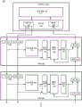
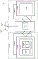
Fig. 1 is a block diagram of an example of an in-memory compute/near-memory computing system that performs computations with dynamically configurable near-memory Computation (CNM) circuitry.
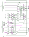
Fig. 2 is a block diagram of an example of a dynamically configurable CNM core.
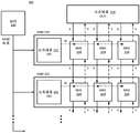
Fig. 3A is a block diagram of an example of a computing operation to configure a dynamically configurable CNM core for matrix-matrix computation.
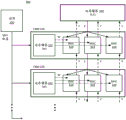
Fig. 3B is a block diagram of an example of a computing operation to configure a dynamically configurable CNM core for matrix-vector computation.
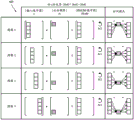
Fig. 4A is a graphical example of a cycle (cycle) of a compute operation with a dynamically configurable CNM core configured for matrix-matrix computation.
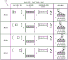
Fig. 4B is a graphical example of a cycle of computational operations with a dynamically configurable CNM core configured for matrix-vector computation.
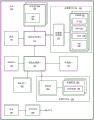
Fig. 5 is a block diagram of an example of a system with a processor and circuitry for compute/near memory computation in dynamically configurable memory.
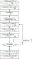
FIG. 6 is a flow diagram of an example of a process for compute/near memory computation in memory with an architecture that can dynamically compute matrix-matrix or matrix-vector computations.
FIG. 7 is a block diagram of an example of a computing system in which in-memory compute/near memory Compute (CIM) operations with a dynamically configurable MAC array can be implemented.
FIG. 8 is a block diagram of an example of a multi-node network in which in-memory compute/near-memory Compute (CIM) operations with a dynamically configurable MAC array can be implemented.
The following is a description of certain details and implementations, including non-limiting descriptions of figures, which may depict some or all examples, as well as other potential implementations.
Detailed Description
As described herein, a memory circuit includes a plurality of multiply-accumulate (MAC) circuits that are dynamically configurable. The MAC circuit or MAC arithmetic unit may be configured to calculate the output based on a calculation of an input vector of X bits and a weight vector, or to calculate the output based on a calculation of an input vector of a single bit and a weight vector. The first memory provides input vectors and the second memory provides weight vectors. Both the input vector and the weight vector may have the same number of bits (e.g., X bits), and depending on the configuration, these bits are delivered and computed in different combinations relative to each other. The MAC circuits are configured in an array, and the configuration can determine the operation of the array. In one example, the array is configured to compute MxV (matrix-vector) computations. In one example, the same array is configured to compute MxM (matrix-matrix) computations.
The dynamic configurability of the MAC array enables the same circuitry to be optimized for either MxM or MxV operations. It will be appreciated that expressions relating to optimization or optimization refer to performance improvements relative to other configurations of circuitry. Such expressions do not necessarily refer to absolute optimality nor imply that additional modifications cannot be made. For example, optimization of MxM operations involves MAC array configuration that improves array performance in relation to configuration that improves performance of MxM operations. Alternatively, a particular configuration may be said to focus on one type of operation or another type of operation, or a configuration may be specific to a particular type of operation. With such configurability, the same circuitry can provide high performance for either type of operation. There will be a cost for this configuration which may reduce performance compared to circuitry optimized separately for a particular type of operation, but which will provide improved performance relative to circuitry configured for one type of operation performing another type of operation. In one example, the reconfigurable MAC array hardware is implemented on dedicated hardware (such as a dedicated processor or accelerator).
Thus, the same circuitry can provide a 2D array configuration for 2D operations to compute a deep learning matrix operation workload for a large number of Neural Network (NN) parameters for inference or training tasks. Similarly, the same circuitry can provide a 1D array configuration that facilitates 1D computational operations. The calculations can include 1D calculations for single or small batches of MLP, RNN and LSTM, where vectors (or narrow matrices) of neuron activations are multiplied by NN weights. The calculation may include 2D calculations for CNNs or large batches of MLPs. In one example, the array configuration for 2D operations or 1D operations can be in the form of a systolic array.
Systolic arrays are understood in the art as modular arrays of similar elements having an architecture that propagates data and results through the array elements before returning to the main processing unit or memory, and will not be described in detail. Much of the description refers to systolic arrays, which will be understood as examples. In certain implementations, systolic array architectures can provide improved performance over non-systolic array architectures, and thus will be used to describe the examples below. Architectures other than systolic arrays may be used. Such architectures can use different types of elements or different arrangements of elements.
Traditional methods of neural network computing include general-purpose multi-core hardware or special-purpose accelerators. General multi-core approaches typically use SIMD (single instruction multiple data) type vectorized, distributed solutions for handling matrix operations, such as on GPU (graphics processing unit) hardware or coprocessor hardware. The general method provides sufficient calculation/bandwidth efficiency for matrix operation; however, they provide lower performance compared to dedicated processors.
Depending on the task and workload chosen, dedicated accelerators (such as stand-alone chips, accelerators, FPGA (field programmable gate array) platforms or other dedicated hardware) typically use arrayed multipliers, such as 2D systolic arrays or 1D computational arrays. Traditional accelerator solutions achieve very energy efficiency for the selected task; however, they suffer from computational or energy efficiency limitations and bandwidth limitations when switching to another task, such as switching from MxM operations to MxV operations. Limited efficiency means that in many implementations, two types of dedicated hardware will be used, which increases cost and reduces overall efficiency, as some hardware inevitably remains unused in certain operations.
With a configurable MAC array, the system can implement a modular near memory Computation (CNM) circuit block as a unified solution for both MxM operations and MxV operations that provides energy efficiency and good computation/bandwidth ratio. The CNM circuit block is an example of a compute/near memory Compute (CIM) circuit in memory. The circuitry may be in-memory computation circuitry including a memory to perform computations. Near memory computation circuitry refers more particularly to CIM circuitry where the memory is a near memory of a multi-level memory architecture, including at least one level of volatile memory having faster access than volatile or non-volatile memory of a far memory level. CIM circuitry is circuitry that enables computational operations to be performed in memory circuitry without having to send data to a processor. The CIM accelerator performs basic operations directly within the memory array, such as dot products and absolute differences of vectors, which reduces the need to transfer data to a compute engine or processor for computation. The reduction of data movement between the memory and the processing unit can be used to speed up memory bandwidth limited algorithms. The reduction of data movement can also reduce data transfer energy overhead. The CIM accelerator based on simulation operations allows (allow for) lower computational cost and higher effective memory bandwidth on a per column access multi-bit data readout.
Integrating lightweight reconfigurable circuits into CNM modules with small near memory and MAC cell arrays enables two different matrix access modes. As a result, the CNM core array may be dynamically configured to execute as a 2D array of MxM operations and as a 1D compute array of MxV operations. Locating the computation near the memory partition maximizes the available local memory bandwidth and minimizes the energy cost of bit transfers for the computation. Reconfigurability of the modular CNM MAC unit allows balancing input, weight, and output reuse based on selected hardware configuration or DNN (deep neural network) characteristics, or both, which can achieve energy efficient gains for various use cases.
The modular nature of the described CNM array enables configurable operation and configurable size for different applications. The configurable array may be applied in any number of computing devices from a server to an edge device. The array is scalable for different applications and flexible for different system uses.
Fig. 1 is a block diagram of an example of an in-memory computing system that performs computations with dynamically configurable near memory Computation (CNM) circuitry. System 100 provides an example of system components that can implement MAC operations on configurable hardware. System 100 includes a common node 110 and a CNM array represented by two CNM cells as shown.
In one example, the common node 110 includes far memory 112, which is a memory resource having a longer access time than near memory. The near memory is co-located with the hardware that will perform the computation, while the far memory has longer access time to the computation hardware than the near memory. Typically, the far memory 112 is larger than the near memory.
In one example, far memory 112 is an SRAM (synchronous random access memory) device. In one example, each near memory 130 is an SRAM device. In one example, the near memory 130 is a register file of a memory device.
In one example, the common node 110 includes control circuitry and various miscellaneous arithmetic logic, or matrix operation logic, or a combination of arithmetic and matrix logic. The logic may be implemented as part of a processor or programmable logic array or as separate hardware. Controller 114 represents logic and control circuitry. The controller 114 may include an interface to compute-in-memory/near memory Compute (CIM) hardware of the CNM array. CIM OUT 116 represents an interface that provides Control (CTRL) and data (X) from far memory 112. Data X from far memory 112 represents one of the operands of the matrix computation to be performed by the CNM array. CIM IN 118 represents an interface that receives data (Y) from the CNM array. Data Y represents the calculation result. The data may be stored in far memory 112.
The common node 110 includes a relatively large memory device that is a far memory 112 for storing X and Y. Near memory 130 is smaller than far memory 112. The controller 114 may be or include one or more control blocks for data communication and access to memory, as well as various arithmetic operations required to implement Deep Neural Network (DNN) machine learning. Depending on the target workload, common node arithmetic operations may include, but are not limited to, element-by-element arithmetic operations, reduction (reduction), pooling (pooling), nonlinear operations, matrix transposition, data reshaping, compression, or a combination of these or other operations. The use of a configurable CNM array is compatible with any design choice of the common node 110 and any arithmetic operations implemented in the common node 110, as long as downstream and upstream control is implemented with CNM cores.
The CNM array includes a plurality of CNM cells or CNM cores identified as CNM 120. The system 100 provides a top-level layout (top-level layout) for the CNM blocks. For any problem size, the matrix and vector may be partitioned into tiles according to the CNM tile size (tile-size) to achieve MxV/MxM with the highest possible utilization. The slice size of the CNM 120 refers to the number of included MAC units. Thus, the example of fig. 2 has 4 MAC units, giving a tile size of 4 and a value of M = 4. V is less than M, such as V = 1.
CNM refers to near memory computing resources where the computing units are integrated directly by memory, or very close to memory. Computing units located near memory provide fine-grained distributed computing and memory arrays. While a typical access to memory will send a command and wait for a data result at the processing core that performs all computations, some computations may be done directly at memory with CNM architecture, reducing the amount of data that needs to be transferred from memory to the processor. Instead, the memory itself has computing resources that can return the results of the computation rather than the data to be used in the computation.
In the configuration of the system 100, the system assigns weights to the near memory 130 at the CNM core of the CNM 120. In one example, the far memory 112 of the common node 110 stores an input matrix (X). Similarly, the output Y matrix is sent back to the common node 110 to be processed or stored in the far memory 112. In one example, all memory accesses within the system 100 are fragmented, with the same address being used for all near memory 130 in each CNM 120. In one example, the common node 110 generates an address or address information to the near memory 130.
In one example, the system 100 sends a small number of addresses and read/write control bits to a downstream data transfer (downlata data transfer) along with the input X vector(s). In one example, CNM 120 passes the same data downstream in a 1D systolic array. As a result of passing the same data downstream, the CNM core will only require lightweight control circuitry to implement the control operation.
CTRL from CIM OUT 116 represents a control bit or command bit from common node 110. CNM 120 includes CMD or command 122, which represents a buffer for control signals. The buffering and forwarding of commands may be similar to that described above with respect to input buffer 124 and input X. In one example, the input X vector(s) may be provided from the input buffer 124 to control hardware indicated as the configuration array 132. In one example, the command causes near memory 130 to generate weight matrix data W to configuration array 132.
The configuration array 132 configures the MAC array 134 for selected operations requested by the common node 110. Configuration array 132 may configure the accumulation operation of MAC array 134. The accumulate operation causes the MAC array to perform an accumulation for a certain number of operations before sending the final accumulated partial product to be written to the PSUM buffer (partial sum buffer) 136. PSUM buffer 136 can implement the upstream transmit partial sum.
The part is sent upstream and the access pattern will depend on the type of operation (matrix-vector or matrix-matrix). CNM 120 transmits the partial sum upstream via the output Y port. In one example, the output Y port is driven by a mux 128, and the mux 128 selects the local portion from the PSUM buffer 136 and the partial sum of the downstream CNM received at the OUT Buff 126. In one example, CNM 120 transmits the partial sum immediately after 1 clock cycle in response to the accumulation signal (part of the control signal-not specifically shown in system 100, but shown in system 200). In one example, the CNM 120 sends the partial sums after the number of clock cycles equals a value indicating the location of the CNM cell in the array. The value indicating the location of a particular CNM unit may be indicated by a number that also indicates the number of MAC units in the MAC array inside each CNM (which may be referred to as a "slice size" in one implementation). After a number of clock cycles of array size or tile size, the CNM cell may output its partial sum.
In one example, after completing the final accumulation, CNM 120 will send out its contents of PSUM buffer 136 and reset the PSUM buffer to 0. A reset after sending out the content enables CNM 120 to be ready for a new set of accumulation operations immediately at the beginning of the next clock cycle. In this way, MAC array 134 can be utilized every clock cycle as long as there is input from the input pipeline. Buffering the input signal IN the IN Buff 124 and the output signal IN the OUT Buff 126 enables the array of CNMs 120 to operate IN a pipelined fashion with one clock cycle of operational delay between adjacent CNM cores IN the 1D systolic array. In one example, if a sufficient amount of in-place (in-place) accumulation is performed in each CNM 120, the outgoing data transmission is collision-free and no additional communication control is required.
The near memory 130 includes an array of memory elements (cells) or bit elements (bitcells). In one example, the array is based on Dynamic Random Access Memory (DRAM) technology. In one example, the array is based on a resistive Random Access Memory (RAM) based element (such as resistive RAM (reram), magnetoresistive RAM (mram), ferroelectric RAM (feram), dielectric RAM or other memory), RAM based on three-dimensional cross-point (3 DXP) phase change, or other byte addressable random access memory technology. In one example, far memory 112 is SRAM based. In one example, far memory 112 is based on one of the other technologies identified above.
In one example, the common node 110 is a hardware platform that includes circuitry and memory near the processor. As such, what is labeled as far memory 112 in system 100 may be a cache or scratch-pad memory of the processor. Far memory 112 is "far" in system 100 relative to MAC computations performed by local memory or near memory 130 located near MAC array 134. As a cache or scratch pad memory, the far memory 112 may actually be a "near memory" with respect to a host processor or host processing unit of a computing device into which the system 100 is incorporated.
A cache memory may refer to a level one memory in a memory hierarchy. Access to cache memory may be constrained by a protocol that defines how memory can be accessed and when and where the access can occur. A scratch pad memory may refer to memory that is similar to a cache, but is randomly accessible by the processor at any time without specific access constraints (e.g., Instruction Set Architecture (ISA) rules) that may apply to the cache. The application of CNM as described may be applied to a cache or scratch pad memory. It will be understood that the application of CNMs to the cache may include the application of certain cache access rules.
In one example, system 100 is integrated on a common die with a host processor, where CNM 120 and its associated memory and MAC units are part of a hardware acceleration circuit. The array of CNMs 120 may be integrated on a hardware accelerator die, which is incorporated on a common substrate or motherboard with a host processor, or included in a system on a chip with a host processor, rather than on a host processor die. Thus, the MAC array may be incorporated on a die with a host processor, or may be implemented off-chip as a hardware accelerator, remote from the processor.
Fig. 2 is a block diagram of an example of a dynamically configurable CNM core. System 200 provides one example of a system in accordance with system 100 of fig. 1. CNM core 210 represents a CNM unit or CNM core of CNM 120 according to fig. 1. In one example, the CNM 210 can be integrated with a larger memory, such as SRAM (static random access memory), DRAM (dynamic random access memory), or other types of memory.
CNM core 210 represents details of an example of a modular CNM core circuit. CNM core 210 includes an input buffer 212 for receiving and distributing input vectors and an input mux or input selector 214. The CNM core 210 includes a Control (CTRL) 216 for configuring the operation of the CNM core according to the received control signal. CNM core 210 includes a near memory (near mem) 220 for locally storing weight data (W), and a mux 222 for providing selected bits to the MAC array. CNM core 210 includes MAC array 230 and partial sum buffer (PSUM) 232. When the computation is complete, the partial sums can be fed back into the MAC array 230 or provided to the output. The CNM core 210 includes an output buffer 240 for receiving and buffering output data from downstream, and a selector or output mux 242 for forwarding local calculations or forwarding data received from downstream. A Control (CTRL) 244 represents control functionality that configures the operation of the output mux 242.
In one example, MAC array 230 includes a plurality of MAC units. In one example, when system 200 is incorporated in a deep learning accelerator that targets inference workload, the MAC unit and accumulation are implemented with integer arithmetic. In one example, when system 200 is incorporated in a deep learning accelerator targeted at training workloads, the CNM computation unit will be constructed with floating point arithmetic. Depending on the target deep learning workload, a single selection of MAC units based on bit precision (e.g., INT32, full precision floating point, or other fixed bit precision), reconfigurable bit precision (e.g., INT8/4/2/1, or other reconfigurable precision), or mixed precision (e.g., bfoat 16/INT8, or other) arithmetic may be implemented in MAC array 230.
As shown, the input buffer 212, near memory 220, MAC array 230, accumulation ("partial sum" or "PSUM") buffer 232, and upstream output buffer 240 match the design choice of M =4, as shown by the 4-element vector. These 4 elements may be referred to as tile sizes, which are values that can be consistent with the input width and output array size. While this example has 4 MAC elements or M =4, it will be appreciated that the system is scalable and may be constructed with more or fewer elements. The use of binary numbers in the array may provide improved efficiency (e.g., with M =2, 4, 8, 16, 32.). The use of binary numbers is not essential and the description should apply to any integer value greater than 1. In one example, there will be multiple CNM cores matching the number of MAC elements in the MAC array within each CNM core 210. Thus, system 200 illustrates an input X [ 3: 0], stored data W [ 3: 0] and in the partial sum Psum [ 3: 0] of a 4-element vector of a MAC array, where the output Y [ 3: 0], where M =4 and the other elements are typically [ (M-1): 0 ]. When a different number of MAC elements is used, the value of M will be correspondingly different. In one example, an element is a bit. In one example, an element is a multi-bit element. As a general example, for X MACs, there will be a pair of X elements, where each element may be a single bit or multiple bits.
Near memory 220 stores a vector of local weights "W" to be buffered in a read port of the memory. In one example, near memory 220 is implemented as a small size memory with high local bandwidth. Examples of memory with high local bandwidth may include Register Files (RF) or small SRAM. Near memory 220 may have single-access capability or multi-port access capability depending on hardware and workload specifications. Thus, near memory 220 may be any of various types of RF, such as 1RW, 1R1W, or other multi-port memory. Alternatively, near memory 220 may be any of a variety of small SRAM variants, such as 1RW, 1R1W, or other multiport memory.
In one example, near memory 220 is used as a timing circuit synchronized with the flip-flops of input buffer 212 to pipeline (pipeline) MAC operations. In one example, mux array 214 is connected to input buffer 212 and mux array 222 is connected to near memory 220. In one example, the input to the mux array is a vector, where the number of elements is equal to the tile size. The output of the mux arrays may be equal length vectors.
The CNM core 210 receives Control (CTRL) bits such as a valid signal, an Accumulate (ACC) signal, an Address (ADR) signal, and one or more other Configuration (CONFIG) bits. The valid signal may be considered a "go" signal for the hardware to perform an operation. The ACC signal may be considered a "complete" signal, meaning that the operation is complete and the accumulated result may be sent. The ADR signal indicates the address of the memory location used in the compute operation. The CONFIG bit may refer to any other signal used to configure the configuration array. The configuration array refers to the component that controls the bit stream to the MAC array 230.
For CNM 210, the system itself does not need to "configure" the circuitry. In one example, by setting one or more configuration or control signals, the bit stream from the input and near memory to the MAC array will change, which changes the operations performed by the MAC array. The bit stream into the MAC array 230 from which the calculations are to be made as input will alter the logical operations performed by the MAC array, even though the MAC array operation is the same in each case. The bits used as input and the number of cycles used for the calculation may determine MxV the difference from the MxM operation. In one example, the MxM operation can be performed in a number of different ways. For example, the configuration of CNM core 210 may be set to provide a different bit to the MAC array for each cycle of operation. Alternatively, the operation of the MxV operations may be extended by repeating the MxV operation pattern multiple times to produce an MxM output. The flexibility of this approach allows the size and operation of the array to be customized according to the problem size and hardware budget to use the same hardware for different operations.
In one example, the configuration signal(s) control the access pattern of the mux array. CNM core 210 receives a control bit at Control (CTRL) 216 to assign a control signal. The logic for control 216 may be simple routing circuitry or a small controller or other circuitry with timing control for the control signals. In one example, control 216 passes an enable signal (EN) to input array 212 and near memory 220. The enable signal enables operation of the near memory and the input buffer, and may be generated in response to a valid signal asserted from upstream. The enable signal may also enable operation of the section and buffer 232.
In one example, mux arrays 214 and 222 implement two specific access modes in response to configuration signal(s): "all to all (all-to-all)" and "one to all (one-to-all)". These two specific access patterns are used in both the MxM operation and the MxV operation. In one example, an "all-to-all" access configuration causes the mux array to pass the vector to its output as is. The vector-as-is delivery delivers different weights to different MAC units. For example, with the tile size selected to be 4, the output vector of the mux array is equal to [ X0, X1, X2, X3] for the input vector of [ X0, X1, X2, X3 ]. In one example, a one-to-all access configuration causes the mux array to pass a single selected element to all output elements. An element that passes a single selection, which is selected by the selection bit "S" of bit width log2 (tile _ size), is transmitted to all compute units, may be referred to as a broadcast. For example, in the case where the tile size is selected to be 4, for "S = 01" of the input vector of [ X0, X1, X2, X3] and the element [ X1] selected at the position <1>, the output vector of the mux array is [ X1, X1, X1, X1 ].
In one example, control 216 includes counter 218 to count from 0 to "tile _ size-1". In one example, CNM core 210 uses counter 218 as an element pointer that controls the select bits "S" of the mux array. In one example, for the MxV access mode, counter 218 implements a pointer for mux array 214 that is connected to input buffer 212. In one example, for the MxV access pattern, the CNM core accesses the near memory 220 every cycle. In one example, for an MxM access mode, counter 218 implements an element pointer for a W vector at a read port of mux array 222 connected to near memory 220. In one example, for the MxM access mode, the CNM core only accesses the near memory 220 once in all cycles of operation, and continues to access the near memory 220 in a continuous manner as new input X vectors continue to arrive each cycle until the accumulation triggers the CNM core 210 to pass results upstream.
In one example, the system 200 pipelines the output of the CNM 210 to enable accumulation of the output of a particular CNM core with results from downstream CNM cores at a common node. Thus, the system 200 can utilize multiple CNM cores 210 or core arrays to provide operation results. The common node is not specifically shown in system 200, but is coupled to the CNM core array. With appropriate hardware in each CNM core, accumulation from downstream may occur in each CNM core. It will be appreciated that such an implementation would require additional circuitry in each core to perform the accumulation. Such hardware is not required in the CNM cores when a common node receives the output from each CNM core and performs an accumulation of all the results. As described, each CNM core can be configured for either 1D or 2D operations. Typically, the array of CNM cores 210 will all be configured for the same type of operation. With CNM core 210, a single hardware core can be used for either the MxV problem or the MxM problem. In both configurations, the CNM core 210 can leverage the MAC array 230. Utilizing all MAC units in each CNM core 210 in each computation cycle maximizes the OPs/W (operations per watt per second) of operation of system 200.
The CNM core 210 enables reconfiguration between 2D and 1D matrix operations on a common hardware accelerator. MAC array 230 is a reconfigurable MAC array with near memory 220 computations. For energy efficiency, near memory 220 is close to (in the same location as) the MAC circuit. In one example, the MAC array 230 includes a standard cell digital MAC unit (cell digital MAC unit). In one example, MAC array 230 includes analog multiplier circuits.
In one example, the system 200 may reconfigure the CNM core 210 into a 1D systolic array for MxV operations. The array need not be pulsed. In one example, system 200 may reconfigure CNM core 210 into a 2D systolic array for MxM operations. The array need not be pulsed. As described above, reconfiguration may be achieved by configuring mux array 214 connected to input buffer 212 and mux array 222 connected to the readers of near memory 220. The configurations for "one to all" and "all to all" can be implemented in mutually exclusive manner. The controls 216 can provide configuration to the mux array or other selector hardware.
As described above, the MAC units of MAC array 230 can be fully utilized in both the MxM configuration and the MxV configuration, and accumulation buffer or PSUM buffer 232 accumulates dot products. In one example, the PSUM buffer 232 is implemented with flip-flops. In one example, PSUM buffer 232 is implemented with latches. The accumulation bit width or the width of the PSUM buffer 232 is selected according to the target problem size. Although 4 elements are illustrated in system 200, it will be understood that PSUM buffer 232 may be wider than the number of bits input. Thus, the 4 elements shown may each hold multiple bits. As a specific example, for a 4-bit input illustrated in system 200, 4 elements of PSUM buffer 232 may hold 32 bits.
In one example, the CNM core 210 includes additional quantization circuitry in addition to standard accumulation circuitry when the output bit width is smaller than the input elements. In such cases, the partial sums can be transmitted directly to the upstream CNM module or common node once the accumulation is complete. To ensure that data transfers occur without collisions, in one example, the output Y vectors received at output port 240 are buffered. Output port 240 is operable as an upstream input buffer for downstream units, and the upstream output is multiplexed with the partial sum of the current core and the input upstream accumulation vector using mux array 242.
In one example, routing and data transfer energy may be minimized by reducing upstream data to send only one element of a core per cycle. Such a configuration reduces the wiring complexity of the system 200 design. In such an implementation, CNM core 210 would need to perform more in-place accumulation before writing the output data back to memory to achieve full utilization of MAC array 230.
In one example, a single bit valid signal can control a read enable bit for near memory 220 and a write enable for input buffer 212. In examples where CNM 210 includes additional flip-flops or buffers for address bits, the valid signal can also control write enable for the address bits. In one example, when the valid bit is high, the valid bit indicates an incoming data transfer (input X and address bits). The dotted line input from the control bit of the CNM core 210 to the output control bit of the CNM core 210 indicates: control bits, including valid bits, may similarly be buffered to an input buffer that enables core-to-core transfer of bits in system 200.
In one example, the accumulated signal is also received as a single bit similar to the valid bit. In one example, the accumulation signal indicates that a final accumulation of dot products is to be performed. Upon receiving the ACC signal, CNM core 210 performs its final accumulation according to the configured access patterns (MxV, MxM) and transmits the partial sum to the upstream output Y port. For MxM, in one example, when the ACC is received, the partial sum is sent out immediately after 1 clock cycle. For MxV, in one example, after the tile _ size number of clock cycles have occurred (e.g., as counted by counter 218), a partial sum is sent out.
In one example, the ACC signals act as mux controls for upstream muxes of mux array 242 to control collisions of upstream communications. In one example, the ACC signal generates a valid signal for outputting a Y data transfer in a manner similar to the way the input valid signal controls the transmission of downstream communications. In one example, the upstream valid signal controls write enable for the output buffer. Since the input and output signals are buffered, cores such as CNM core 210 can operate in a pipelined fashion. With pipelined operation, the system 200 may have one clock cycle operation delay between adjacent CNM cores in a 1D core array of the system 200. If a sufficient number of in-place accumulations are performed in each CNM core, the output data transfer is collision-free and no additional communication control will be required.
Fig. 3A is a block diagram of an example of a computing operation to configure a dynamically configurable CNM core for matrix-matrix computation. System 302 illustrates a two-dimensional (2D) systolic array for MxM operations according to the system of system 100 of fig. 1. The 2D systolic configuration of system 302 is a configuration of modular, reconfigurable hardware according to system 200 of fig. 2.
The system 302 includes a large far memory 310 to store matrix operands (X) and matrix results (Y). Control 330 configures CNM 320 for MxM operations in system 302. MxM config represents one or more control signals that control the hardware of CNM 320 to control the operation of the MAC unit in response to inputs. Controls 330 represent hardware that provides configuration to the CNM 320. It will be appreciated that the control 330 can be implemented at least partially inside the CNM 320.
Far memory 310 broadcasts element X to the 2D array of CNM 320 in a row-by-row manner and a column-by-column manner. The broadcast of X is illustrated by separate solid lines to each MAC unit 324. Further, W is passed from near memory 322 to all MAC units 324. The CNM is caused to receive input and operate on it in an MxM manner based on the configuration of controls 330. The elements of X may be referred to as input activation data. Row/column elements are passed from one CNM 320 to the next in the same row-by-row/column-by-column direction to maximize data reuse and amortize the high energy cost of memory access.
Each calculation unit CNM 320 performs a MAC operation with the MAC unit 324 while MAC accumulates partial sums. The MAC unit 324 represents an array of parallel MAC arithmetic units. CNM 320 performs MAC operations on X received from far memory 310 and W accessed from near memory 322. W denotes locally stored weight data. In system 302, CNM 320 performs MAC operations as a 2D array, where a single W element is broadcast to all MAC units 324 within the CNM core and multiplied by multiple X elements. In one example, for a received slice size number of X vectors, the near memory 322 is only accessed once and repeated in the same manner until a final accumulation is performed and Y is sent to the far memory 310.
It will be appreciated that MAC unit 324 includes a summation circuit not specifically shown in system 302. After multiple accumulations, MAC unit 324 sends the final dot product result back to far memory 310 to be stored. Whether selected by a system designer or to meet application requirements, system 302 is compatible with any of a variety of different arithmetic design choices. For example, MAC unit 324 may be implemented with integer arithmetic or floating point arithmetic, and MAC unit 324 may be based on fixed bit precision, reconfigurable bit precision, or mixed precision. The MAC unit 324 is illustrated as a MAC without explicit bit precision. Similarly, system 302 is compatible with different vector sizes and assumes that the bit widths of the X and W vectors match the arithmetic criteria specified as a design choice for the compute unit and not specifically indicated.
Fig. 3B is a block diagram of an example of a computing operation to configure a dynamically configurable CNM core for matrix-vector computation. System 304 illustrates a one-dimensional (1D) systolic array for MxV operations according to the system of system 100 of fig. 1. The 1D systolic configuration of system 304 is the configuration of reconfigurable hardware according to system 200 of fig. 2. System 304 is an alternative configuration of the hardware of system 302. Thus, the hardware description of far memory 310, CNM 320, near memory 322, MAC 324, and controls 330 will not be repeated here, but rather understood to be the same as that of system 302.
Control 330 configures CNM 320 for MxV operations in system 304. MxV config represents one or more control signals that control the hardware of CNM 320 to control the operation of the MAC unit in response to inputs. While system 302 is configured as a 2D array, system 304 is configured as a 1D array for MxV operations. The 1D array approach can maximize data reuse of vector elements. Far memory 310 broadcasts element X to the 1D array of CNM 320. MAC unit 324 performs computations based on X from far memory 310 and matrix operands accessed from local memory banks (local memory banks) of near memory 322. The MAC unit 324 is a 1D computational array that performs MAC operations in which partial sums are accumulated and the final dot product is sent back to the far memory 310 to be stored.
In one example, for the MxV configuration of system 304, control 330 configures CNM 320 to execute as a 1D computational array, where multiple W elements read from near memory 322 are assigned to parallel MAC units 324 and multiplied by a single X element received from far memory 310. A single X-ray from far memory 310 to CNM 320 represents the use of a single X-ray, as opposed to a different X-ray as in system 302. System 304 can assign different W elements to the MAC unit for operation, as shown by the parallel W lines. As with the 2D configuration of system 302, the 1D configuration of system 304 can leverage MAC units.
Each calculation unit CNM 320 performs a MAC operation with the MAC unit 324 while MAC accumulates partial sums. The MAC unit 324 represents an array of parallel MAC arithmetic units. CNM 320 performs MAC operations on X received from far memory 310 and W accessed from near memory 322. W denotes locally stored weight data.
The configuration of system 302 or the application of the configuration of system 304 will depend on the particular workload to be computed. It will be appreciated that different configurations will have different power results depending on the operation. Different configurations will provide better performance in different environments.
The operation performed will produce one column of output per input (for the MxM operation) or one row of output per input (for the MxV operation). Although the outputs are different, it will be understood that the hardware has no orientation. Rather, the hardware simply generates an output in response to the input, and the output may be interpreted based on the type of operation to be performed.
It will be appreciated that the hardware of systems 302 and 304 will suffer compared to conventional circuits that only perform MxM operations or MxV operations. For example, a circuit that only performs MxM operations would be more efficient than system 302 for MxM operations, but if MxV operations would need to be performed, it would be less efficient, and system 302 might be reconfigured into system 304 for MxV operations. Alternatively, a circuit that only performs MxV operations would be more efficient than system 304 for MxV operations, but if MxM operations would need to be performed, it would be less efficient and system 304 could be reconfigured into system 302 for MxM operations.
Fig. 4A is a graphical example of a cycle of computational operations with a dynamically configurable CNM core configured for matrix-matrix computation. Table 400 illustrates MxM access patterns of reconfigurable CNM cores in accordance with system 100 and system 200.
Table 400 shows an access mode configuration for an MxM operation of an example slice size of 4. The elements of input X are stored in the input buffer while W is accessed from near memory. The partial sums are accumulated in a PSUM buffer. The illustrated example performs an MxM operation of the form [4X4] × [4X4] = [4X4], where the input X received column by column to the input buffer is a matrix of size [4X4], the weight matrix accessed from near memory is of size [4X4], and the output Y accumulated column by column on the PSUM buffer is a matrix of size [4X4 ].
The MxM operation is configured as a relative access pattern of MxV (as shown in table 410 of fig. 4B). In one example, a mux array connected to an input buffer is configured for all to all access modes. When deploying a CNM core, the access pattern configures the CNM array as a 2D array. For an example tile size of 4, table 400 shows the dot product of a single column of the output Y matrix during an MxM operation in 4 clock cycles. In cycle 0, column 0 of input X is multiplied by bit 0 of weight vector W. In cycle 1, column 1 of input X is multiplied by bit 1 of weight vector W. In cycle 2, column 2 of input X is multiplied by bit 2 of weight vector W. In cycle 3, column 3 of input X is multiplied by bit 3 of weight vector W. For this example, column 0 of the W matrix stored in near memory is accessed once at the initial clock and is used repeatedly for 4 cycles. As a result, one column of the X matrix is sent as a vector to the MAC array at each cycle.
In this way, each clock cycle implements multiplication and accumulation of a single W element with one column of the X matrix. At the end of each cycle, the partial sums are accumulated in the PSUM buffer. As a result, the product [4x4] × [4x1] = [4x1] is realized in the CNM core in 4 clock cycles, thereby fully utilizing the MAC array in each cycle. For this example, successive columns of the output matrix Y are computed by repeating the 4 clock cycle operation shown in FIG. 4A for successive W columns, the output matrix Y being computed in 16 cycles, since the subsequent clock cycles will compute different elements of the input and near memories until the entire matrix is computed. For example, cycle 4-7 will compute the second column of output Y with the next element of W, continuing until the computation is completed.
Fig. 4B is a graphical example of a cycle of computational operations with a dynamically configurable CNM core configured for matrix-vector computation. Table 410 illustrates MxV access patterns according to reconfigurable CNM cores of system 100 and system 200.
Table 410 shows an access pattern configuration for an MxV operation of example slice size 4. The elements of input X are stored in the input buffer while W is accessed from near memory. The partial sums are accumulated in a PSUM buffer. The illustrated example performs a MxV operation of the form [1X4] × [4X4] = [1X4], where the input X is a vector of size [1X4], the weight matrix accessed from near memory is of size [4X4], and the output Y accumulated on the PSUM buffer is of size [1X4 ].
MxV operations are configured as relative access patterns of MxM (as shown in table 400 of FIG. 4A). In one example, a mux array connected to an input buffer is configured into one to all access modes. This access pattern configures the CNM array as a 1D array when the CNM cores are deployed. For an example slice size of 4, table 410 shows MxV operations implemented in the CNM core at 4 clock cycles. In one example, the input X vector elements are accessed in 4 consecutive cycles and broadcast to the MAC array. In one example, the W matrix is stored in row-first (row-major) format, and a single readout from near memory provides one row of the W matrix, which is a W row vector of size [1 × tile _ size =4 ]. Thus, at each successive cycle, one row of the W matrix is read out and sent to the MAC array.
In cycle 0, one bit of input X is multiplied by row 0 of weight vector W. In cycle 1, one bit of input X is multiplied by row 1 of weight vector W. In cycle 2, one bit of input X is multiplied by row 2 of weight vector W. In cycle 3, one bit of input X is multiplied by row 3 of weight vector W. As a result, the product [1x4] × [4x4] = [1x4] is realized in the CNM core in 4 clock cycles, thereby fully utilizing the MAC array in each cycle. For this example, input X accesses one element per clock cycle while reusing the same input X vector received at the initial clock cycle.
It will be observed that the MxV operation shown in table 410 may also be repeated to implement the MxM operation. The energy benefits and cost of performing the repeated MxV operations, as opposed to the MxM operations according to table 400, depend on specific hardware choices, such as CNM near memory 130 and common node far memory 112 size, available BW, number of CNM cores in the 1D array, deep neural network parameters, and other considerations.
Fig. 5 is a block diagram of an example of a system with a processor and circuitry for compute/near memory computation in dynamically configurable memory. System 500 may include CIM circuitry with reconfigurable CNM circuitry according to any of the examples described above. The CIM circuitry may be a CIM accelerator for machine learning or other computationally intensive operations. The accelerator may be referred to as a coprocessor.
The system 500 includes a processor 510, which may be or include a general purpose CPU (central processing unit), GPU (graphics processing unit), DSP (digital signal processor) array or other processor. Processor 510 represents a digital processor and may be referred to as a host processor. In one example, processor 510 includes a plurality of cores 512. The processor 510 executes an application or software program that accesses data for computationally intensive operations.
In one example, processor 510 includes a first level cache 514, which represents a cache resource within a processor die or processor SOC (System on a chip) that provides a physically close storage resource for thermal data. In one example, processor 510 includes multiple levels of on-chip/local caches, not explicitly shown. It will be appreciated that the cache resources may be local resources to a particular core 512, shared by multiple cores 512, or a combination of shared and localized cache resources.
Operand fetch 566 represents the fetching or obtaining of operands to be executed upon by an instruction. In one example, the operand is a weight vector for a neural network, or other mathematical function operand. In one example, operands are in or are placed in register space associated with the execution pipeline. Execution 568 refers to executing the instruction on or with the operand(s). In one example, executing may include sending the operation to CIM circuitry for execution. In one example, instructions are sent to a processor ALU (arithmetic logic unit), which may trigger execution of the CIM accelerator. Write back 570 refers to writing the execution results into a result register for return to memory, or to passing to another register for another execution. Where CIM circuitry is used, executing 568 and writing back 570 may include sending the operation to the CIM circuitry, which will execute the operation and return the functional output, which may then be written back. The performing may include configuration of CNM circuitry according to any example described herein. Thus, instructions that would traditionally require operands to be loaded into the ALUs or other compute engines within the processor 510 may be sent to the CIM circuitry without having to read from memory, and then receive the computed results from the CIM circuitry rather than from the local compute engines.
In one example, the invocation of the compute-intensive function triggers the directing of a command to the CIM accelerator. For example, the processor 510 may include support in its Instruction Set Architecture (ISA) for certain commands that trigger operation of the CIM accelerator. In one example, invocation of the CIM accelerator may precede or be associated with loading configuration information into the accelerator. Such configuration information may, for example, define the weight of the internode connection, define the mathematical function to be performed, or other configuration. The system 500 may load configuration information from main system memory or from non-volatile mass storage, or a combination thereof.
In one example, CIM circuitry of CIM 530 or CIM 540 or both may include one or more stages of neural networks. In one example, after configuring the CIM circuitry, the instruction pipeline applies the input values to the configured neural network for processing. The CIM circuitry generates results that are written back to register space or system memory, and the CIM circuitry may indicate completion of processing to the executing thread that called the CIM circuitry. In one example, if the number of neural network levels or neurons per level that are physically implemented in CIM circuitry is less than the number of levels/neurons of the neural network to be processed, the processing through the neural network may be iterated by repeatedly loading CIM circuitry for processing until all levels of the neural network have been processed.
FIG. 6 is a flow diagram of an example of a process for computation in memory with an architecture that can dynamically compute matrix-matrix or matrix-vector computations. Process 600 represents a process for MAC computation with a configurable MAC array according to any of the descriptions herein. In one example, a system including a configurable MAC array determines whether to perform an MxM calculation or an MxV calculation (block 602). The determination may be based on a matrix workload for the neural network operation to be performed. In one example, the system generates a configuration bit (block 604), such as where the master controller sends a control bit that the control logic on the CNM core will use for the configuration operation.
In one example, the CNM unit configures the MAC array in response to the configuration bits (block 606). The CNM unit accesses one or more far memory bit inputs X (block 608). The CNM cell also accesses one or more near memory bit inputs W (block 610). The CNM unit calculates the product of X W with the configured MAC array (block 612).
In one example, the MAC array continues to perform multiply and accumulate operations until a completion signal is received. If the CNM unit is to continue accumulating the partial sum information ("yes" branch of block 614), the MAC unit performs the accumulation (block 616) and returns to accessing one or more far memory bits (block 608). It will be appreciated that in iterations after accumulation, accessing far or near memory may refer to accessing data from a buffer, rather than accessing a particular memory device again.
Once all the accumulation operations are completed ("no" branch of block 614), the CNM unit may send the resultant data bit vector Y upstream (block 618). The system may apply the result bits to the final operation to generate the desired output (block 620).
FIG. 7 is a block diagram of an example of a computing system in which in-memory Computation (CIM) operations with dynamically configurable MAC arrays may be implemented. System 700 represents a computing device according to any example herein, and can be a laptop computer, desktop computer, tablet computer, server, gaming or entertainment control system, scanner, copier, printer, routing or switching device, embedded computing device, smartphone, wearable device, internet of things device, or other electronic device.
In one example, system 700 includes CIM circuitry. The CIM circuitry includes reconfigurable CNM circuitry according to any of the examples described herein. One example of CIM circuitry may be CIM 792, which is represented as CIM circuitry included in processor SOC 710. CIM 792 may be or include CIM circuitry in a memory device on a processor SOC substrate or die. For example, the CIM 792 may be part of a cache on the processor SOC 710. Another example of CIM circuitry may be CIM 794, which is represented as CIM circuitry included in memory subsystem 720. More specifically, CIM 794 is illustrated as part of memory 730, referring to memory resources of system 700. CIM 794 represents CIM circuitry that may be included as a memory resource to which processor SOC 710 may offload compute-intensive operations. The compute intensive operations may include MxM operations and MxV operations. The configurable CNM circuitry enables CIM 792 or CIM 794 to be configurable for both types of workloads. The circuitry is dynamically configured according to the operation to be performed.
The system 700 includes a processor SOC 710 (hereinafter "processor 710") that provides processing, operational management, and instruction execution for the system 700. Processor 710 may include any type of microprocessor, Central Processing Unit (CPU), Graphics Processing Unit (GPU), processing core, or other processing hardware, or combination of processors, that provides processing for system 700. Processors 710 may include a single core or multiple cores. Processor 710 controls the overall operation of system 700 and may be or include one or more programmable general purpose or special purpose microprocessors, Digital Signal Processors (DSPs), programmable controllers, Application Specific Integrated Circuits (ASICs), Programmable Logic Devices (PLDs), and the like, or a combination of such devices.
In one example, system 700 includes an interface 712 coupled to processor 710, which may represent a higher speed interface or a high throughput interface for system components that require higher bandwidth connections, such as memory subsystem 720 or graphics interface component 740. Interface 712 represents an interface circuit that may be a separate component or integrated onto the processor die. Where present, the graphical interface 740 interfaces to graphical components for providing visual displays to a user of the system 700. In one example, the graphical interface 740 may drive a High Definition (HD) display that provides output to a user. High definition may refer to displays having a pixel density of approximately 100 PPI (pixels per inch) or greater, and may include formats such as full HD (e.g., 1080 p), retinal display (retina display), 4K (ultra high definition or UHD), or others. In one example, the display may comprise a touch screen display. In one example, the graphics interface 740 generates a display based on data stored in the memory 730 or based on operations performed by the processor 710, or both.
Memory subsystem 720 represents the main memory of system 700 and provides storage for code to be executed by processor 710 or data values to be used in executing routines. Memory subsystem 720 may include one or more memory devices 730, such as Read Only Memory (ROM), flash memory, one or more Random Access Memories (RAMs) such as DRAM, or other memory devices or combinations of such devices. Memory 730 stores and hosts, among other things, an Operating System (OS) 732 to provide a software platform for execution of instructions in system 700. Further, applications 734 may execute on the software platform of OS 732 from memory 730. Applications 734 represent executing programs with their own operating logic to perform one or more functions. Process 736 represents an agent or routine that provides ancillary functionality to OS 732 or one or more applications 734, or a combination thereof. The OS 732, applications 734, and processes 736 provide software logic to provide functionality for the system 700. In one example, memory subsystem 720 includes memory controller 722, which is a memory controller that generates and issues commands to memory 730. It will be appreciated that memory controller 722 may be a physical part of processor 710 or a physical part of interface 712. For example, memory controller 722 may be an integrated memory controller, integrated onto a circuit with processor 710.
Although not specifically illustrated, it will be understood that the system 700 may include one or more buses or bus systems, such as a memory bus, a graphics bus, an interface bus, or other buses, between the devices. A bus or other signal line may communicatively or electrically couple the components together or both. A bus may include physical communication lines, point-to-point connections, bridges, adapters, controllers, or other circuitry, or a combination thereof. A bus may include, for example, one or more of the following: a system bus, a Peripheral Component Interconnect (PCI) bus, a hyper transport or Industry Standard Architecture (ISA) bus, a Small Computer System Interface (SCSI) bus, a Universal Serial Bus (USB), or an Institute of Electrical and Electronics Engineers (IEEE) standard 1394 bus.
In one example, system 700 includes an interface 714, which can be coupled to interface 712. Interface 714 may be a lower speed interface than interface 712. In one example, interface 714 represents interface circuitry, which may include stand-alone components and integrated circuitry. In one example, a plurality of user interface components or peripheral components or both are coupled to the interface 714. Network interface 750 provides system 700 with the ability to communicate with remote devices (e.g., servers or other computing devices) over one or more networks. Network interface 750 may include an ethernet adapter, a wireless interconnection component, a cellular network interconnection component, a USB (universal serial bus) or other interface or proprietary interface based on a wired or wireless standard. Network interface 750 may exchange data with remote devices, which may include transmitting data stored in memory or receiving data to be stored in memory.
In one example, system 700 includes one or more input/output (I/O) interfaces 760. The I/O interface 760 can include one or more interface components through which a user interacts with the system 700 (e.g., audio, alphanumeric, tactile/touch or other interface connection). Peripheral interface 770 may include any hardware interface not specifically mentioned above. Peripherals generally refer to devices that are subordinately connected to system 700. A slave connection is a connection in which the system 700 provides a software platform or a hardware platform or both, on which operations are performed, and with which a user interacts.
In one example, the system 700 includes a storage subsystem 780 that stores data in a nonvolatile manner. In one example, in some system implementations, at least some components of memory subsystem 780 may overlap with components of memory subsystem 720. Storage subsystem 780 includes storage 784(s), which may be or include any conventional medium for storing large amounts of data in a non-volatile manner, such as one or more magnetic, solid-state, or optical based disks or a combination thereof. The storage 784 holds the code or instructions and data 786 in a persistent state (i.e., the value is retained despite a power interruption to the system 700). Although memory 730 is typically the execution or manipulation memory that provides instructions to processor 710, storage 784 may generally be considered "memory". Although storage 784 is non-volatile, memory 730 may include volatile memory (i.e., the state or value of data is indeterminate if power is interrupted to system 700). In one example, storage subsystem 780 includes a controller 782 that interfaces with a storage 784. In one example, controller 782 is a physical part of interface 714 or processor 710, or may comprise circuitry or logic in both processor 710 and interface 714.
A power supply 702 provides power to the components of the system 700. More specifically, the power supply 702 is typically interfaced to one or more power supplies 704 in the system 700 to provide power to the components of the system 700. In one example, the power supply 704 includes an AC-to-DC (alternating current to direct current) adapter to plug into a wall outlet. Such AC power may be a renewable energy (e.g., solar) power source 702. In one example, the power supply 702 includes a DC power supply, such as an external AC to DC converter. In one example, the power source 702 or power supply 704 includes wireless charging hardware that charges via a proximity charging field. In one example, the power source 702 may include an internal battery or fuel cell source.
FIG. 8 is a block diagram of an example of a multi-node network in which in-memory Computation (CIM) operations with dynamically configurable MAC arrays may be implemented. System 800 represents a network of nodes according to any example described herein. In one example, system 800 represents a data center. In one example, system 800 represents a server farm (server farm). In one example, system 800 represents a data cloud or processing cloud.
Node 830 includes memory 840, which in one example comprises a CIM 842. The CIM circuitry includes reconfigurable CNM circuitry according to any of the examples described herein. With CIM 842, memory 840 becomes a computing resource for node 830. More specifically, CIM 842 enables node 830 to provide improved processing for memory/data-intensive and compute-intensive workloads. Instead of moving data back and forth from memory to processor, the CIM 842 enables memory to perform calculations and return functional results to the calling processor 832. CIM 842 may be implemented as a separate resource within memory 840 or as an accelerator. In one example, CIM 842 is implemented as a cache on processor 832. In one example, CIM 842 is a separate blade that is an accelerator for a blade (blade) of a processor resource. Depending on the type of workload to be performed, the configurable CNM circuitry enables CIM 842 to be configured for either MxM operations or MxV operations. The circuitry is dynamically configured according to the operation to be performed.
One or more clients 802 make requests to system 800 via network 804. Network 804 represents one or more local area networks, or wide area networks, or a combination. The client 802, which may be a human or machine client, generates requests to perform operations by the system 800. The system 800 performs application or data computing tasks requested by the client 802.
In one example, system 800 includes one or more racks (racks) representing fabric and interconnect resources that house and interconnect a plurality of compute nodes. In one example, the chassis 810 includes a plurality of nodes 830. In one example, the chassis 810 hosts a plurality of blade assemblies 820. Hosting refers to providing electrical power, structural or mechanical support, and interconnection. Blade 820 may refer to a computing resource on a Printed Circuit Board (PCB), where the PCB houses the hardware components of one or more nodes 830. In one example, blades 820 do not include a chassis or enclosure or other "box" in addition to the chassis (chassis) or enclosure or other "box" provided by chassis 810. In one example, blade 820 includes a housing having exposed connectors that connect into chassis 810. In one example, system 800 does not include chassis 810, and each blade 820 includes a chassis or enclosure that can be stacked or otherwise reside near other blades and allow nodes 830 to be interconnected.
As shown, the chassis 810 includes N blades 820. In one example, system 800 includes a chassis 850 in addition to chassis 810. As shown, the chassis 850 includes M blades 860. M is not necessarily the same as N; thus, it will be appreciated that a variety of different hardware device components may be used and coupled together into system 800 by fabric 870. Blade 860 may be the same or similar to blade 820. The nodes 830 may be any type of node and are not necessarily all the same type of node. The system 800 is not limited to homogeneous (homogenes) nor heterogeneous.
For simplicity, only the nodes in blade 820[0] are illustrated in detail. However, other nodes in system 800 may be the same or similar. At least some of the nodes 830 are compute nodes having a processor (proc) 832 and a memory 840. A compute node refers to a node having processing resources (e.g., one or more processors) that execute an operating system and can receive and process one or more tasks. In one example, at least some of the nodes 830 are server nodes, with servers as processing resources represented by processors 832 and memory 840. A storage server refers to a node that has more storage resources than compute nodes, and the storage server includes processing resources that manage access to the storage nodes within the storage server, without having processors to perform tasks.
In one example, the node 830 includes an interface controller 834, which represents logic that controls access to the fabric 870 by the node 830. The logic may include hardware resources interconnected with physical interconnect hardware. The logic may include software or firmware logic to manage the interconnect. In one example, the interface controller 834 is or includes a host fabric interface, which may be a fabric interface according to any of the examples described herein.
References to memory devices may be applicable to different memory types. Memory devices generally relate to volatile memory technology. Volatile memory is memory whose state (and thus the data stored thereon) is indeterminate if power is interrupted to the device. Non-volatile memory refers to memory whose state is determined even if power to the device is interrupted. Dynamic volatile memories require refreshing of data stored in the device to maintain state. One example of dynamic volatile memory includes DRAM (dynamic random access memory), or some variant, such as synchronous DRAM (sdram). The memory subsystem as described herein is compatible with a number of memory technologies, such as DDR3 (double data Rate version 3 JESD79-3 originally published by JEDEC (Joint electronic device engineering Commission) at 6 months 2007), DDR4 (DDR version 4 JESD79-4, the initial specification published by JEDEC at 9 months 2012), LPDDR3 (Low Power DDR version 3 JESD209-3 at 8 months 2013 of JEDEC), LPDDR4 (LPDDR version 4 JESD209-4 originally published by JEDEC at 8 months 2014), WIO2 (Wide I/O2 (Wideio 2) JESD-2 originally published by JEDEC at 8 months 2014), HBM (high Bandwidth SD235 originally published by JEDEC at 10 months 2013), DDR5 (currently discussed by DDR DEC version 5), LPDD 5 (LPDD version 209-3, currently discussed by JEDEC 209-3), LPDD version 209-4 originally published by JEDEC at 2015), or other memory technologies or combinations thereof, as well as derived or extended technologies based on such specifications.
Generally, with respect to the description herein, in one example, an apparatus comprises: providing a first memory having an input vector of width X elements; and an on-chip multiply-accumulate (MAC) array having the first memory, the MAC array comprising: a second memory storing the weight vector; and X MAC circuits dynamically configurable to: the output is calculated based on the calculation of the X elements of the input vector and the weight vector, or the output is calculated based on the calculation of a single element of the input vector and the weight vector.
In one example, the first memory includes a Static Random Access Memory (SRAM). In one example, the second memory includes a register file. In one example, the second memory includes a Static Random Access Memory (SRAM). In one example, the MAC array is on a common memory die with a first memory, wherein the first memory is a cache memory of a processor. In one example, the MAC array is on a common memory die with a first memory, where the first memory is a scratch pad memory of the processor. In one example, the MAC array is within a system on a chip having a first memory, wherein the first memory is a cache memory of a processor. In one example, the MAC array is within a system on a chip having a first memory, wherein the first memory is a scratch pad memory of the processor. In one example, the MAC array further comprises: a multiplexer (mux) providing an alternate path between the first memory and the MAC array; and a mux controller that controls the mux to select between the alternate paths. In one example, the mux controller calculates for one dimension (1D) MxV to control the mux for one input vector element to all X MAC circuits. In one example, a mux controller calculates, for a two-dimensional (2D) MxM, to control a mux for X different input vector elements to the X MAC circuits, respectively.
Generally, with respect to the description herein, in one example, a system comprises: providing a scratch pad memory having processing units with input vectors of width X elements; and a hardware accelerator coupled to a scratch pad memory of the processing unit, the hardware accelerator comprising in-memory compute/near memory Compute (CIM) circuitry having a multiply-accumulate (MAC) array, the MAC array comprising: a local memory storing the weight vector; and X MAC circuits dynamically configurable to: the output is calculated based on the calculation of the X elements of the input vector and the weight vector, or the output is calculated based on the calculation of a single element of the input vector and the weight vector.
In one example, the cache or scratch pad memory includes Static Random Access Memory (SRAM). In one example, the local memory includes a register file. In one example, the local memory includes Static Random Access Memory (SRAM). In one example, the hardware accelerator is integrated on a common memory die with a cache or scratch pad memory. In one example, the hardware accelerator is integrated on a system on chip with the cache or scratch pad memory. In one example, the MAC array further comprises: a multiplexer (mux) that provides an alternate path between the cache or scratch pad memory and the MAC array; and a mux controller that controls the mux to select between the alternate paths. In one example, the mux controller computes, for one dimension (1D) MxV, all X MAC circuits that are to control the mux for one input vector element to the MAC array. In one example, a mux controller computes, for a two-dimensional (2D) MxM, X MAC circuits to control a mux for X different input vector elements, respectively, to a MAC array. In one example, wherein: the processing unit comprises a multi-core host processor device; the system further includes a display communicatively coupled to the host processor; the system further includes a network interface communicatively coupled to the host processor; or the system further comprises a battery for powering the system.
The flow diagrams as illustrated herein provide examples of sequences of various process actions. The flow diagrams may indicate operations to be performed by software or firmware routines, as well as physical operations. The flow diagrams may illustrate examples of implementations of states of a Finite State Machine (FSM), which may be implemented in hardware and/or software. Although shown in a particular order or sequence, the order of the actions can be modified unless otherwise specified. Thus, the illustrated figures should be understood only as examples, and the process can be performed in a different order, and some actions may be performed in parallel. Further, one or more actions may be omitted; thus, not all implementations will perform all actions.
To the extent that various operations or functions are described herein, they may be described or defined as software code, instructions, configurations, and/or data. The content may be directly executable ("object" or "executable" form), source code, or differential code ("delta" or "patch" code). The software content described herein can be provided via an article of manufacture (article of manufacture) having the content stored thereon, or via a method of operating a communication interface to send data via the communication interface. A machine-readable storage medium may cause a machine to perform the functions or operations described, and includes any mechanism (mechanism) that stores information in a form accessible by a machine (e.g., a computing device, an electronic system, etc.), such as recordable/non-recordable media (e.g., Read Only Memory (ROM), Random Access Memory (RAM), magnetic disk storage media, optical storage media, flash memory devices, etc.). A communication interface includes any mechanism that interfaces with any of a hardwired, wireless, optical, etc. medium to communicate with another device (such as a memory bus interface, a processor bus interface, an internet connection, a disk controller, etc.). The communication interface may be configured by providing configuration parameters and/or sending signals to prepare the communication interface to provide data signals describing the software content. The communication interface may be accessed via one or more commands or signals sent to the communication interface.
The various components described herein may be means for performing the operations or functions described. Each component described herein includes software, hardware, or a combination of these. A component can be implemented as a software module, a hardware module, dedicated hardware (e.g., application specific hardware, Application Specific Integrated Circuit (ASIC), Digital Signal Processor (DSP), etc.), embedded controller, hardwired circuitry, or the like.
Various modifications can be made to the implementations of the invention and the disclosure without departing from their scope, in addition to those described herein. Accordingly, the illustrations and examples herein should be construed in an illustrative, and not a restrictive, sense. The scope of the invention should be measured solely by reference to the claims that follow.
Claims (16)
1. An apparatus for multiply-accumulate (MAC) operations, comprising:
a first memory for providing an input vector having a width of X elements; and
an on-chip multiply-accumulate (MAC) array having the first memory, the MAC array comprising:
a second memory for storing a weight vector; and
x MAC circuits dynamically configurable to: calculating an output based on the calculation of the X elements of the input vector and the weight vector, or calculating the output based on the calculation of a single element of the input vector and the weight vector.
2. The apparatus of claim 1, wherein the MAC array is on a common memory die with the first memory, wherein the first memory is a cache memory of a processor.
3. The apparatus of claim 1, wherein the MAC array is on a common memory die with the first memory, wherein the first memory is a scratch pad memory of a processor.
4. The apparatus of claim 1, wherein the MAC array is within a system on a chip having the first memory, wherein the first memory is a cache memory of a processor.
5. The apparatus of claim 1, wherein the MAC array is within a system on a chip having the first memory, wherein the first memory is a scratch pad memory of a processor.
6. The apparatus of any of claims 1 to 5, the MAC array further comprising:
a multiplexer (mux) to provide an alternate path between the first memory and the MAC array; and
a mux controller to control the mux to select between the alternate paths.
7. The apparatus of claim 6 wherein the mux controller calculates, for one dimension (1D) MxV, to control the mux for one input vector element to all X MAC circuits.
8. The apparatus of claim 6, wherein the mux controller is to control the mux for X different input vector elements to the X MAC circuits, respectively, for a two-dimensional (2D) MxM calculation.
9. The apparatus of any of claims 1-8, wherein the first memory comprises a Static Random Access Memory (SRAM).
10. The apparatus of any of claims 1-8, wherein the second memory comprises a register file.
11. The apparatus of any of claims 1-10, wherein the second memory comprises a Static Random Access Memory (SRAM).
12. A system for multiply-accumulate (MAC) operations, comprising:
a scratch pad memory of a processing unit to provide an input vector having a width of X elements; and
a hardware accelerator coupled to the scratch pad memory of the processing unit, the hardware accelerator comprising in-memory compute/near-memory Compute (CIM) circuitry having a multiply-accumulate (MAC) array, the MAC array comprising:
a local memory for storing a weight vector; and
x MAC circuits that are dynamically configurable to: calculating an output based on the calculation of the X elements of the input vector and the weight vector, or calculating the output based on the calculation of a single element of the input vector and the weight vector.
13. The system of claim 12, the MAC array further comprising:
a multiplexer (mux) to provide an alternate path between the scratch pad memory and the MAC array; and
a mux controller to control the mux to select between the alternate paths.
14. The system of claim 13 wherein the mux controller computes, for one dimension (1D) MxV, all X MAC circuits to control the mux for one input vector element to the MAC array.
15. The system of claim 13, wherein the mux controller is to control the mux for X different input vector elements to the X MAC circuits of the MAC array, respectively, for a two-dimensional (2D) MxM calculation.
16. The system of claim 12, wherein:
the processing unit comprises a multi-core host processor device;
the system further includes a display communicatively coupled to the host processor;
the system further includes a network interface communicatively coupled to the host processor; or
The system further includes a battery to power the system.
Applications Claiming Priority (2)
| Application Number | Priority Date | Filing Date | Title |
|---|---|---|---|
| US16/586,648 US11347477B2 (en) | 2019-09-27 | 2019-09-27 | Compute in/near memory (CIM) circuit architecture for unified matrix-matrix and matrix-vector computations |
| US16/586648 | 2019-09-27 |
Publications (1)
| Publication Number | Publication Date |
|---|---|
| CN112579043A true CN112579043A (en) | 2021-03-30 |
Family
ID=69161884
Family Applications (1)
| Application Number | Title | Priority Date | Filing Date |
|---|---|---|---|
| CN202010578598.8A Pending CN112579043A (en) | 2019-09-27 | 2020-06-23 | Compute/near memory Compute (CIM) circuit architecture in memory |
Country Status (3)
| Country | Link |
|---|---|
| US (1) | US11347477B2 (en) |
| CN (1) | CN112579043A (en) |
| DE (1) | DE102020122174A1 (en) |
Cited By (6)
| Publication number | Priority date | Publication date | Assignee | Title |
|---|---|---|---|---|
| CN115346573A (en) * | 2021-07-23 | 2022-11-15 | 台湾积体电路制造股份有限公司 | Memory device and method of operating the same |
| CN115344528A (en) * | 2021-05-13 | 2022-11-15 | 联咏科技股份有限公司 | In-memory computing macro device and electronic device |
| CN115729861A (en) * | 2021-08-31 | 2023-03-03 | 美光科技公司 | In-memory association processing for vectors |
| TWI796977B (en) * | 2021-11-22 | 2023-03-21 | 旺宏電子股份有限公司 | Memory device and operation method thereof |
| CN117561519A (en) * | 2021-06-29 | 2024-02-13 | 高通股份有限公司 | In-memory computing architecture for depth-wise convolutions |
| TWI842375B (en) * | 2022-03-03 | 2024-05-11 | 台灣積體電路製造股份有限公司 | Method for reading memory and memory device |
Families Citing this family (49)
| Publication number | Priority date | Publication date | Assignee | Title |
|---|---|---|---|---|
| KR102778192B1 (en) | 2018-12-03 | 2025-03-10 | 삼성전자주식회사 | Semiconductor memory device employing processing in memory (PIM) and operating method for the same |
| CN111382094B (en) * | 2018-12-29 | 2021-11-30 | 深圳云天励飞技术有限公司 | Data processing method and device |
| US11455368B2 (en) | 2019-10-02 | 2022-09-27 | Flex Logix Technologies, Inc. | MAC processing pipeline having conversion circuitry, and methods of operating same |
| US11908541B2 (en) * | 2020-01-07 | 2024-02-20 | SK Hynix Inc. | Processing-in-memory (PIM) systems |
| US12386777B2 (en) | 2020-01-07 | 2025-08-12 | SK Hynix Inc. | Processing-in-memory (PIM) device to perform a memory access operation and an arithmetic operation in response to a command from a PIM controller and a high speed interface, respectively |
| US20230025899A1 (en) * | 2020-01-07 | 2023-01-26 | SK Hynix Inc. | Processing-in-memory(pim) device |
| US12136470B2 (en) | 2020-01-07 | 2024-11-05 | SK Hynix Inc. | Processing-in-memory (PIM) system that changes between multiplication/accumulation (MAC) and memory modes and operating methods of the PIM system |
| US12417075B2 (en) * | 2020-01-07 | 2025-09-16 | SK Hynix Inc. | Processing-in-memory (PIM) devices |
| CN115461712A (en) * | 2020-02-05 | 2022-12-09 | 普林斯顿大学理事会 | Scalable array architecture for in-memory computation |
| US11249723B2 (en) * | 2020-04-02 | 2022-02-15 | Micron Technology, Inc. | Posit tensor processing |
| US12627726B2 (en) | 2020-04-09 | 2026-05-12 | Micron Technology, Inc. | Edge server with deep learning accelerator and random access memory |
| US11461651B2 (en) | 2020-04-09 | 2022-10-04 | Micron Technology, Inc. | System on a chip with deep learning accelerator and random access memory |
| US11442881B2 (en) * | 2020-04-18 | 2022-09-13 | Flex Logix Technologies, Inc. | MAC processing pipelines, circuitry to control and configure same, and methods of operating same |
| US11450672B2 (en) * | 2020-04-27 | 2022-09-20 | Intel Corporation | Ultra-deep compute static random access memory with high compute throughput and multi-directional data propagation |
| DE102020131666A1 (en) * | 2020-05-05 | 2021-11-11 | Intel Corporation | Scalable multiplication acceleration of sparse matrices using systolic arrays with feedback inputs |
| US11216373B2 (en) | 2020-05-29 | 2022-01-04 | Advanced Micro Devices, Inc. | Memory access commands with near-memory address generation |
| US12327175B2 (en) | 2020-08-06 | 2025-06-10 | Micron Technology, Inc. | Collaborative sensor data processing by deep learning accelerators with integrated random access memory |
| US11347652B2 (en) * | 2020-08-31 | 2022-05-31 | Microsoft Technology Licensing, Llc | Banked memory architecture for multiple parallel datapath channels in an accelerator |
| TWI777645B (en) * | 2020-09-08 | 2022-09-11 | 旺宏電子股份有限公司 | Memory device and operation method thereof |
| US11809838B2 (en) | 2020-09-08 | 2023-11-07 | Macronix International Co., Ltd. | Memory device and operation method thereof |
| US12504958B2 (en) | 2020-09-09 | 2025-12-23 | Ascenium, Inc. | Compute element processing using control word templates |
| US12493554B2 (en) | 2020-09-09 | 2025-12-09 | Ascenium, Inc. | Parallel processing using hazard detection and mitigation |
| US12578991B2 (en) | 2020-09-09 | 2026-03-17 | Ascenium, Inc. | Parallel processing architecture with distributed register files |
| EP4229572A4 (en) * | 2020-10-15 | 2024-11-20 | Ascenium, Inc. | Parallel processing architecture with background loads |
| US12093802B2 (en) | 2020-10-20 | 2024-09-17 | International Business Machines Corporation | Gated unit for a gated recurrent neural network |
| US11513893B2 (en) | 2020-12-21 | 2022-11-29 | Intel Corporation | Concurrent compute and ECC for in-memory matrix vector operations |
| US12147784B2 (en) * | 2021-01-29 | 2024-11-19 | Taiwan Semiconductor Manufacturing Company, Ltd. | Compute in memory |
| TWI775402B (en) * | 2021-04-22 | 2022-08-21 | 臺灣發展軟體科技股份有限公司 | Data processing circuit and fault-mitigating method |
| US12106822B2 (en) * | 2021-07-16 | 2024-10-01 | Mediatek Singapore Pte. Ltd. | Memory array with programmable number of filters |
| US12373686B2 (en) * | 2021-09-10 | 2025-07-29 | Samsung Electronics Co., Ltd. | Methods of operating an artificial neural network using a compute-in-memory accelerator and a bitwise activation function |
| CN115964014A (en) * | 2021-10-12 | 2023-04-14 | 北京苹芯科技有限公司 | floating point unit |
| US12118060B2 (en) * | 2021-12-08 | 2024-10-15 | Tenstorrent Inc. | Computational circuit with hierarchical accumulator |
| US12235756B2 (en) * | 2021-12-21 | 2025-02-25 | Advanced Micro Devices, Inc. | Approach for performing efficient memory operations using near-memory compute elements |
| WO2023158858A1 (en) * | 2022-02-21 | 2023-08-24 | Flex Logix Technologies, Inc. | Broadcast data, shared weight multiply-accumulate |
| US20230297335A1 (en) * | 2022-03-15 | 2023-09-21 | Qualcomm Incorporated | Hybrid Compute-in-Memory |
| US12456043B2 (en) * | 2022-03-31 | 2025-10-28 | International Business Machines Corporation | Two-dimensional mesh for compute-in-memory accelerator architecture |
| CN115658013B (en) * | 2022-09-30 | 2023-11-07 | 杭州智芯科微电子科技有限公司 | ROM in-memory computing device of vector multiply adder and electronic equipment |
| US20240171192A1 (en) * | 2022-11-10 | 2024-05-23 | Micron Technology, Inc. | Encode Inputs to Reduce Energy Usages in Analog Computation Acceleration |
| CN121153019A (en) * | 2023-03-16 | 2025-12-16 | 美光科技公司 | Near-memory pseudo-random number generation |
| WO2024253750A1 (en) * | 2023-06-05 | 2024-12-12 | Rain Neuromorphics Inc. | Architecture for ai accelerator platform |
| CN121729699A (en) | 2023-06-14 | 2026-03-24 | 睿纽摩菲斯公司 | Training optimization for low memory occupancy |
| KR20240175962A (en) | 2023-06-14 | 2024-12-23 | 삼성전자주식회사 | Digital signal processor and electronic apparatus using the same |
| CN121713172A (en) | 2023-06-23 | 2026-03-20 | 睿纽摩菲斯公司 | Flexible Computing Engine Microarchitecture |
| US20250028674A1 (en) * | 2023-07-19 | 2025-01-23 | Rain Neuromorphics Inc. | Instruction set architecture for in-memory computing |
| US12536118B2 (en) | 2023-07-31 | 2026-01-27 | Rain Neuromorphics Inc. | Tiled in-memory computing architecture |
| US20250307180A1 (en) * | 2024-03-27 | 2025-10-02 | Advanced Micro Devices, Inc. | Software Runtime Assisted Co-Processing Acceleration with a Memory Hierarchy Augmented with Compute Elements |
| US20250307343A1 (en) * | 2024-03-29 | 2025-10-02 | Microsoft Technology Licensing, Llc | Tensor processing unit with configurable hardware |
| US20260079714A1 (en) * | 2024-09-19 | 2026-03-19 | Arm Limited | Data processing array |
| EP4726564A1 (en) * | 2024-10-10 | 2026-04-15 | STMicroelectronics International N.V. | Shared routing and sensing in a multi-tile digital in-memory computation (dimc) neural processing unit (npu) |
Family Cites Families (16)
| Publication number | Priority date | Publication date | Assignee | Title |
|---|---|---|---|---|
| US8832530B2 (en) | 2012-09-26 | 2014-09-09 | Intel Corporation | Techniques associated with a read and write window budget for a two level memory system |
| EP3025239B1 (en) | 2013-07-26 | 2018-12-26 | Intel Corporation | Non-volatile memory interface |
| US11055063B2 (en) * | 2016-05-02 | 2021-07-06 | Marvell Asia Pte, Ltd. | Systems and methods for deep learning processor |
| US10509738B2 (en) * | 2016-07-01 | 2019-12-17 | Intel Corporation | Remote memory operations |
| WO2019114842A1 (en) * | 2017-12-14 | 2019-06-20 | 北京中科寒武纪科技有限公司 | Integrated circuit chip apparatus |
| US11580353B2 (en) * | 2018-05-04 | 2023-02-14 | Apple Inc. | Neural network processor for handling differing datatypes |
| US11262982B2 (en) * | 2018-07-23 | 2022-03-01 | SK Hynix Inc. | Computation circuit including a plurality of processing elements coupled to a common accumulator, a computation device and a system including the same |
| US10754649B2 (en) * | 2018-07-24 | 2020-08-25 | Apple Inc. | Computation engine that operates in matrix and vector modes |
| US10748603B2 (en) * | 2018-09-28 | 2020-08-18 | Intel Corporation | In-memory multiply and accumulate with global charge-sharing |
| KR102771073B1 (en) * | 2019-02-08 | 2025-02-19 | 삼성전자주식회사 | A memory device and a computing device using the same |
| US20190227750A1 (en) * | 2019-03-29 | 2019-07-25 | Intel Corporation | Technologies for performing tensor operations in memory |
| US11531898B2 (en) * | 2019-05-16 | 2022-12-20 | International Business Machines Corporation | Training of artificial neural networks |
| KR102727600B1 (en) * | 2019-07-08 | 2024-11-07 | 에스케이하이닉스 주식회사 | Data storing device, Data Processing System and accelerating DEVICE therefor |
| US10977002B2 (en) * | 2019-07-15 | 2021-04-13 | Facebook Technologies, Llc | System and method for supporting alternate number format for efficient multiplication |
| US11449739B2 (en) * | 2019-08-22 | 2022-09-20 | Google Llc | General padding support for convolution on systolic arrays |
| US11726950B2 (en) * | 2019-09-28 | 2023-08-15 | Intel Corporation | Compute near memory convolution accelerator |
-
2019
- 2019-09-27 US US16/586,648 patent/US11347477B2/en active Active
-
2020
- 2020-06-23 CN CN202010578598.8A patent/CN112579043A/en active Pending
- 2020-08-25 DE DE102020122174.6A patent/DE102020122174A1/en active Pending
Cited By (7)
| Publication number | Priority date | Publication date | Assignee | Title |
|---|---|---|---|---|
| CN115344528A (en) * | 2021-05-13 | 2022-11-15 | 联咏科技股份有限公司 | In-memory computing macro device and electronic device |
| CN117561519A (en) * | 2021-06-29 | 2024-02-13 | 高通股份有限公司 | In-memory computing architecture for depth-wise convolutions |
| CN115346573A (en) * | 2021-07-23 | 2022-11-15 | 台湾积体电路制造股份有限公司 | Memory device and method of operating the same |
| CN115729861A (en) * | 2021-08-31 | 2023-03-03 | 美光科技公司 | In-memory association processing for vectors |
| CN115729861B (en) * | 2021-08-31 | 2025-12-23 | 美光科技公司 | In-memory association processing for vectors |
| TWI796977B (en) * | 2021-11-22 | 2023-03-21 | 旺宏電子股份有限公司 | Memory device and operation method thereof |
| TWI842375B (en) * | 2022-03-03 | 2024-05-11 | 台灣積體電路製造股份有限公司 | Method for reading memory and memory device |
Also Published As
| Publication number | Publication date |
|---|---|
| DE102020122174A1 (en) | 2021-04-01 |
| US11347477B2 (en) | 2022-05-31 |
| US20200026498A1 (en) | 2020-01-23 |
Similar Documents
| Publication | Publication Date | Title |
|---|---|---|
| US11347477B2 (en) | Compute in/near memory (CIM) circuit architecture for unified matrix-matrix and matrix-vector computations | |
| US11893424B2 (en) | Training a neural network using a non-homogenous set of reconfigurable processors | |
| US11847395B2 (en) | Executing a neural network graph using a non-homogenous set of reconfigurable processors | |
| US20240112006A1 (en) | Deep learning hardware | |
| CN111859273B (en) | Matrix Multiplier | |
| CN110352435B (en) | Neural network processing using chained instructions | |
| KR102955942B1 (en) | Neural network accelerator with parameters resident on chip | |
| JP7262569B2 (en) | Matrix-vector multiplier with vector register file with multiport memory | |
| US12436901B2 (en) | Controlling access to a memory shared by a cluster of multiple processing elements | |
| US11443014B1 (en) | Sparse matrix multiplier in hardware and a reconfigurable data processor including same | |
| TWI784845B (en) | Dataflow function offload to reconfigurable processors | |
| US11580397B2 (en) | Tensor dropout using a mask having a different ordering than the tensor | |
| CN111079908A (en) | Network-on-chip data processing method, storage medium, computer device and apparatus | |
| US12189569B1 (en) | Distributive training with multicast | |
| Liang et al. | Design of 16-bit fixed-point CNN coprocessor based on FPGA | |
| CN114661345A (en) | Acceleration operation device and method, integrated circuit chip, calculation device and board card | |
| US20240086257A1 (en) | Direct dataflow compute-in-memory accelerator interface and architecture | |
| CN114565075B (en) | Device, method and readable storage medium supporting multiple access modes | |
| Demler | Flex Logix Moves Into Chips | |
| CN121745180A (en) | RISC-V-based neural network accelerator design method and system |
Legal Events
| Date | Code | Title | Description |
|---|---|---|---|
| PB01 | Publication | ||
| PB01 | Publication | ||
| SE01 | Entry into force of request for substantive examination | ||
| SE01 | Entry into force of request for substantive examination |