CN109065469B - Take laser cutting function's IC chip optics to take out machine of examining - Google Patents
Take laser cutting function's IC chip optics to take out machine of examining Download PDFInfo
- Publication number
- CN109065469B CN109065469B CN201810585880.1A CN201810585880A CN109065469B CN 109065469 B CN109065469 B CN 109065469B CN 201810585880 A CN201810585880 A CN 201810585880A CN 109065469 B CN109065469 B CN 109065469B
- Authority
- CN
- China
- Prior art keywords
- chip
- guide rail
- platform
- motor
- microscope
- Prior art date
- Legal status (The legal status is an assumption and is not a legal conclusion. Google has not performed a legal analysis and makes no representation as to the accuracy of the status listed.)
- Active
Links
Images


Classifications
-
- H—ELECTRICITY
- H10—SEMICONDUCTOR DEVICES; ELECTRIC SOLID-STATE DEVICES NOT OTHERWISE PROVIDED FOR
- H10P—GENERIC PROCESSES OR APPARATUS FOR THE MANUFACTURE OR TREATMENT OF DEVICES COVERED BY CLASS H10
- H10P72/00—Handling or holding of wafers, substrates or devices during manufacture or treatment thereof
- H10P72/06—Apparatus for monitoring, sorting, marking, testing or measuring
- H10P72/0611—Sorting devices
-
- B—PERFORMING OPERATIONS; TRANSPORTING
- B07—SEPARATING SOLIDS FROM SOLIDS; SORTING
- B07C—POSTAL SORTING; SORTING INDIVIDUAL ARTICLES, OR BULK MATERIAL FIT TO BE SORTED PIECE-MEAL, e.g. BY PICKING
- B07C5/00—Sorting according to a characteristic or feature of the articles or material being sorted, e.g. by control effected by devices which detect or measure such characteristic or feature; Sorting by manually actuated devices, e.g. switches
- B07C5/02—Measures preceding sorting, e.g. arranging articles in a stream orientating
-
- B—PERFORMING OPERATIONS; TRANSPORTING
- B07—SEPARATING SOLIDS FROM SOLIDS; SORTING
- B07C—POSTAL SORTING; SORTING INDIVIDUAL ARTICLES, OR BULK MATERIAL FIT TO BE SORTED PIECE-MEAL, e.g. BY PICKING
- B07C5/00—Sorting according to a characteristic or feature of the articles or material being sorted, e.g. by control effected by devices which detect or measure such characteristic or feature; Sorting by manually actuated devices, e.g. switches
- B07C5/34—Sorting according to other particular properties
- B07C5/342—Sorting according to other particular properties according to optical properties, e.g. colour
- B07C5/3422—Sorting according to other particular properties according to optical properties, e.g. colour using video scanning devices, e.g. TV-cameras
-
- B—PERFORMING OPERATIONS; TRANSPORTING
- B07—SEPARATING SOLIDS FROM SOLIDS; SORTING
- B07C—POSTAL SORTING; SORTING INDIVIDUAL ARTICLES, OR BULK MATERIAL FIT TO BE SORTED PIECE-MEAL, e.g. BY PICKING
- B07C5/00—Sorting according to a characteristic or feature of the articles or material being sorted, e.g. by control effected by devices which detect or measure such characteristic or feature; Sorting by manually actuated devices, e.g. switches
- B07C5/36—Sorting apparatus characterised by the means used for distribution
- B07C5/361—Processing or control devices therefor, e.g. escort memory
- B07C5/362—Separating or distributor mechanisms
-
- H—ELECTRICITY
- H10—SEMICONDUCTOR DEVICES; ELECTRIC SOLID-STATE DEVICES NOT OTHERWISE PROVIDED FOR
- H10P—GENERIC PROCESSES OR APPARATUS FOR THE MANUFACTURE OR TREATMENT OF DEVICES COVERED BY CLASS H10
- H10P72/00—Handling or holding of wafers, substrates or devices during manufacture or treatment thereof
- H10P72/06—Apparatus for monitoring, sorting, marking, testing or measuring
- H10P72/0614—Marking devices
-
- H—ELECTRICITY
- H10—SEMICONDUCTOR DEVICES; ELECTRIC SOLID-STATE DEVICES NOT OTHERWISE PROVIDED FOR
- H10P—GENERIC PROCESSES OR APPARATUS FOR THE MANUFACTURE OR TREATMENT OF DEVICES COVERED BY CLASS H10
- H10P72/00—Handling or holding of wafers, substrates or devices during manufacture or treatment thereof
- H10P72/06—Apparatus for monitoring, sorting, marking, testing or measuring
- H10P72/0616—Monitoring of warpages, curvatures, damages, defects or the like
-
- H—ELECTRICITY
- H10—SEMICONDUCTOR DEVICES; ELECTRIC SOLID-STATE DEVICES NOT OTHERWISE PROVIDED FOR
- H10P—GENERIC PROCESSES OR APPARATUS FOR THE MANUFACTURE OR TREATMENT OF DEVICES COVERED BY CLASS H10
- H10P72/00—Handling or holding of wafers, substrates or devices during manufacture or treatment thereof
- H10P72/06—Apparatus for monitoring, sorting, marking, testing or measuring
- H10P72/0618—Apparatus for monitoring, sorting, marking, testing or measuring using identification means, e.g. labels on substrates or labels on containers
Landscapes
- Engineering & Computer Science (AREA)
- Multimedia (AREA)
- Investigating Materials By The Use Of Optical Means Adapted For Particular Applications (AREA)
Abstract
Description
技术领域technical field
本发明涉及一种芯片抽检机,具体涉及一种带激光切割功能的IC芯片光学抽检机。The invention relates to a chip sampling inspection machine, in particular to an IC chip optical sampling inspection machine with a laser cutting function.
背景技术Background technique
电子芯片封装前需要对线弧、焊球等进行检验,避免线弧和焊球缺陷对芯片性能和良率的影响。芯片条带封装前不能用手接触,否则容易造成人为的对芯片二次损坏。传统的芯片条带检验,都是检验人员用手拉动芯片条带到显微镜下观察,对于有质量缺陷的芯片元件,还需要人为手工勾线弧,也就造成了手接触芯片条带,对芯片条带的二次损坏;另外,人眼长期在显微镜下观察,容易疲倦,损伤眼睛。Before packaging electronic chips, it is necessary to inspect wire arcs, solder balls, etc. to avoid the influence of wire arc and solder ball defects on chip performance and yield. Before the chip strip is packaged, it should not be touched by hand, otherwise it will easily cause secondary damage to the chip. In the traditional chip strip inspection, the inspector pulls the chip strip by hand to observe it under the microscope. For the chip components with quality defects, it is necessary to manually hook the arc, which causes the hand to touch the chip strip, and the chip The secondary damage of the strip; in addition, the human eye is easy to get tired and damage the eyes after long-term observation under the microscope.
发明内容SUMMARY OF THE INVENTION
针对上述存在的问题,本发明提供了一种带激光切割功能的IC芯片光学抽检机,在检查的过程中,不用手去触碰芯片条带,避免对芯片条带的二次损坏;对于有缺陷的芯片不用手工处理,而是采用激光进行切割或打标,进一步避免人工处理过程中,手对芯片的接触,对芯片造成二次伤害。为了避免人眼长时间观看显微镜疲惫,本发明在显微镜的目镜处安装了CCD相机,CCD相机和监视画面显示器相连,这样在芯片条带检验过程中检验人员只用观看监视画面显示器,相比直接用显微镜的目镜观察,眼睛不易疲劳,降低了检验人员的工作强度。In view of the above existing problems, the present invention provides an IC chip optical sampling inspection machine with a laser cutting function. During the inspection process, the chip strip is not touched by hand, so as to avoid secondary damage to the chip strip; Defective chips do not need to be processed manually, but are cut or marked by laser, which further avoids the contact between hands and chips during manual processing, which will cause secondary damage to the chips. In order to avoid the fatigue of human eyes watching the microscope for a long time, a CCD camera is installed at the eyepiece of the microscope, and the CCD camera is connected to the monitoring screen display, so that the inspector only needs to watch the monitoring screen display during the chip strip inspection process. Observed with the eyepiece of the microscope, the eyes are not easy to fatigue, and the work intensity of the inspector is reduced.
本发明采用的技术方案如下:The technical scheme adopted in the present invention is as follows:
一种带激光切割功能的IC芯片光学抽检机,其特征在于,包括架体和安装在架体上的料盒机构、推料机构、取料机构、运输机构、显微镜机构、激光切割机构,料盒机构的位置能上下、X方向、Y方向调节;推料机构能将料盒机构中的芯片条带从料盒机构中推出;取料机构能将被推料机构推出的芯片条带夹取到运输机构上;运输机构能将芯片条带运送到显微镜机构下观察或运送到激光切割机构下切割或打标。An IC chip optical sampling machine with laser cutting function is characterized in that it includes a frame body and a material box mechanism, a material pushing mechanism, a material reclaiming mechanism, a transport mechanism, a microscope mechanism, and a laser cutting mechanism installed on the frame body. The position of the box mechanism can be adjusted up and down, in the X direction and the Y direction; the push mechanism can push the chip strip in the box mechanism out of the box mechanism; the take-up mechanism can clamp the chip strip pushed out by the push mechanism To the transport mechanism; the transport mechanism can transport the chip strip to the microscope mechanism for observation or to the laser cutting mechanism for cutting or marking.
本发明在芯片条带检验过程中,芯片条带的选择、运输、观察、处理,全过程都不需要用手接触芯片条带,避免了对芯片的人为二次损坏。In the process of chip strip inspection, the invention does not need to touch the chip strip by hand in the whole process of selection, transportation, observation and processing of the chip strip, thereby avoiding artificial secondary damage to the chip.
更进一步, 料盒机构包括X方向调节机构一、Y方向调节机构一、上下调节机构、料盒本体,X方向调节机构一能调节料盒本体在X方向上的位置;Y方向调节机构一能调节料盒本体在Y方向上的位置;上下调节机构能调节料盒本体的上下位置。Further, the material box mechanism includes an X-direction adjustment mechanism, a Y-direction adjustment mechanism, a vertical adjustment mechanism, and a material box body. The X-direction adjustment mechanism can adjust the position of the material box body in the X direction; the Y-direction adjustment mechanism can adjust the position of the material box body. Adjust the position of the material box body in the Y direction; the up and down adjustment mechanism can adjust the up and down position of the material box body.
料盒本体为多层,在选定检验某层的芯片条带后,料盒机构的位置能够灵活调节,以便推料机构能准确推到选定层数的芯片条带。The material box body is multi-layered. After selecting and inspecting a certain layer of chip strips, the position of the material box mechanism can be flexibly adjusted, so that the pushing mechanism can accurately push the chip strips of the selected layers.
更进一步,推料机构包括固定在架体上的支架、推针气缸、推针装置,推针气缸和推针装置安装在支架上,推针气缸能带动推针装置移动推动芯片条带。Furthermore, the pushing mechanism includes a bracket fixed on the frame body, a pin-push cylinder, and a pin-push device. The pin-push cylinder and the pin-push device are mounted on the bracket, and the pin-push cylinder can drive the pin-push device to move and push the chip strip.
更进一步,推针装置包括安装在支架上的轨道二、支架二,支架二在推针气缸的作用下能在轨道二上滑动;支架二上安装有固定块,固定块与推针气缸连接,推针穿过固定块与缓冲器相连,缓冲器固定在支架二上;推料异常检测装置能检测缓冲器受到的压力。Further, the needle pushing device includes a second track and a second bracket installed on the bracket, and the second bracket can slide on the second track under the action of the needle pushing cylinder; The push pin is connected with the buffer through the fixing block, and the buffer is fixed on the second bracket; the abnormality detection device of the push material can detect the pressure on the buffer.
缓冲器包括壳体和安装在壳体内的弹簧,推料异常检测装置能检测到弹簧受到的压力,从而判断推针是否对准芯片条带。The buffer includes a casing and a spring installed in the casing, and the abnormal pusher detection device can detect the pressure on the spring, so as to determine whether the push pin is aligned with the chip strip.
更进一步,运输机构包括安装在架体上的平台装置、安装在平台装置上的导轨装置,平台装置能在X方向和Y方向上移动;导轨装置的宽度可以根据芯片条带的宽度调节。Furthermore, the transport mechanism includes a platform device mounted on the rack body and a guide rail device mounted on the platform device, the platform device can move in the X direction and the Y direction; the width of the guide rail device can be adjusted according to the width of the chip strip.
平台装置能在X方向和Y方向上移动,以便将芯片条带运送到显微镜机构下或激光切割机构下进行处理。导轨装置的宽度可以根据芯片条带的宽度调节,以便轨道适用于不同宽度的芯片条带。The platform device can be moved in the X and Y directions to transport the chip strips to be processed under the microscope mechanism or the laser cutting mechanism. The width of the rail device can be adjusted according to the width of the chip strips, so that the rails are suitable for different widths of the chip strips.
更进一步,平台装置包括平台、平台X电机、平台Y电机,平台Y电机固定安装在架体上,平台Y电机的输出端和Y丝杠的一端连接,Y丝杠的另一端穿过滑动件;滑动件上固定有平台X电机,平台X电机的输出端和X丝杆的一端连接,X丝杆的另一端和平台连接;导轨装置包括固定导轨、滑动导轨、导轨电机,固定导轨和导轨电机固定安装在平台上,导轨丝杆的一端和导轨电机连接,导轨丝杆的另一端穿过滑动导轨;导轨电机转动能带动滑动导轨移动。Further, the platform device includes a platform, a platform X motor, and a platform Y motor, the platform Y motor is fixedly installed on the frame body, the output end of the platform Y motor is connected to one end of the Y lead screw, and the other end of the Y lead screw passes through the sliding piece. ;The platform X motor is fixed on the sliding part, the output end of the platform X motor is connected with one end of the X screw rod, and the other end of the X screw rod is connected with the platform; the guide rail device includes a fixed guide rail, a sliding guide rail, a guide rail motor, a fixed guide rail and a guide rail The motor is fixedly installed on the platform, one end of the guide rail screw is connected with the guide rail motor, and the other end of the guide rail screw passes through the sliding guide rail; the rotation of the guide rail motor can drive the sliding guide rail to move.
利用丝杆滑块结构调整滑动导轨的位置,从而调整导轨装置的宽度,以适应不同宽度的芯片条带。The position of the sliding guide rail is adjusted by the screw-slider structure, so as to adjust the width of the guide rail device to adapt to the chip strips of different widths.
更进一步,取料机构安装在平台上,取料机构包括取料机械手、取料电机,取料电机的输出端和链条连接,取料机械手和链条连接,链条转动能带动取料机械手在取料导轨上滑动。Further, the reclaiming mechanism is installed on the platform. The reclaiming mechanism includes a reclaiming manipulator and a reclaiming motor. The output end of the reclaiming motor is connected with the chain, and the reclaiming manipulator is connected with the chain. The rotation of the chain can drive the reclaiming manipulator to reclaim the material. slide on rails.
更进一步,显微镜、安装在显微镜下的旋转台、安装在旋转台下的光源,旋转台能在旋转电机的驱动下在水平方向上旋转,旋转台中安装有能在竖直方向上旋转的反光镜,显微镜和旋转台的竖直距离可以调节;显微镜的目镜处安装有CCD相机,CCD相机和监视画面显示器相连。Further, the microscope, the rotating stage installed under the microscope, and the light source installed under the rotating stage, the rotating stage can be rotated in the horizontal direction under the drive of the rotating motor, and a reflector that can rotate in the vertical direction is installed in the rotating stage. , the vertical distance between the microscope and the rotating stage can be adjusted; a CCD camera is installed at the eyepiece of the microscope, and the CCD camera is connected with the monitor screen display.
旋转台的旋转配合反光镜的旋转,可以对芯片进行360的观察,其中侧面观察解决了芯片Die熔浆爬升高度和线弧Wire在正面观察中不易观察的问题,让检验更加准确方便。利用CCD相机和监视画面显示器,检验员在检验芯片条带的时候,不用直接通过显微镜目镜观察,通过监视画面显示器就能完成观察,更加方便。The rotation of the turntable and the rotation of the reflector allow 360-degree observation of the chip. The side observation solves the problem that the chip Die melt climbing height and the arc wire are difficult to observe in the frontal observation, making the inspection more accurate and convenient. Using the CCD camera and the monitoring screen display, the inspector does not need to observe directly through the microscope eyepiece when inspecting the chip strip, but can complete the observation through the monitoring screen display, which is more convenient.
更进一步,显微镜安装在升降机构上,升降机构能调节显微镜与旋转台的竖直距离;升降机构安装在架体上;芯片抽检机还包括二维码扫描机构、与控制器连接的操作界面显示器。Further, the microscope is installed on the lifting mechanism, which can adjust the vertical distance between the microscope and the rotating table; the lifting mechanism is installed on the frame; the chip sampling machine also includes a two-dimensional code scanning mechanism and an operation interface display connected to the controller. .
二维码扫描机构可以读取芯片条带上的二维码,操作界面显示器可以显示执行的命令。The two-dimensional code scanning mechanism can read the two-dimensional code on the chip strip, and the operation interface display can display the executed commands.
更进一步,激光切割机构包括振镜和光纤激光器,光纤激光器安装在架体上,振镜和光纤激光器连接。Further, the laser cutting mechanism includes a galvanometer and a fiber laser, the fiber laser is installed on the frame, and the galvanometer and the fiber laser are connected.
采用振镜和光纤激光器相结合的方式,可以对检验到不良的芯片Die和线弧Wire进行切割,或在旁边进行打标标记。Using the combination of galvanometer and fiber laser, the defective chip Die and arc wire can be cut, or marked on the side.
综上所述,本发明的有益效果是:To sum up, the beneficial effects of the present invention are:
1. 本发明在芯片条带检验过程中,芯片条带的选择、运输、观察、处理,全过程都不需要用手接触芯片条带,避免了对芯片的人为二次损坏;1. In the process of chip strip inspection of the present invention, the selection, transportation, observation and processing of the chip strip do not require hand contact with the chip strip in the whole process, which avoids artificial secondary damage to the chip;
2. 料盒机构的位置能够灵活调节,以便推料机构能准确推到选定层数的芯片条带;2. The position of the material box mechanism can be adjusted flexibly, so that the pushing mechanism can accurately push the chip strip with the selected number of layers;
3.推针装置的位置可以上下、X方向、Y方向调节,以适应不同的料盒大小;3. The position of the needle pushing device can be adjusted up and down, in the X direction and in the Y direction to adapt to different box sizes;
4. 导轨装置的宽度可以根据芯片条带的宽度调节,以便轨道适用于不同宽度的芯片条带;4. The width of the guide rail device can be adjusted according to the width of the chip strip, so that the track is suitable for chip strips of different widths;
5. 旋转台的旋转配合反光镜的旋转,可以对芯片进行360的观察,其中侧面观察解决了芯片Die熔浆爬升高度和线弧Wire在正面观察中不易观察的问题,让检验更加准确方便;5. The rotation of the turntable cooperates with the rotation of the mirror to observe the chip 360 degrees. The side observation solves the problem that the die melt climbing height of the chip and the arc wire are difficult to observe in the frontal observation, which makes the inspection more accurate and convenient;
6.本发明采用激光对芯片条带进行芯片Die和线弧Wire的切割或打标,相比传统用手工钩线弧,避免了对芯片的二次人为接触损坏;6. The present invention uses laser to cut or mark the chip die and the wire arc on the chip strip. Compared with the traditional manual hooking and arc, the secondary human contact damage to the chip is avoided;
7. 利用CCD相机和监视画面显示器,检验员在检验芯片条带的时候,不用直接通过显微镜目镜观察,通过监视画面显示器就能完成观察,更加方便;7. Using the CCD camera and the monitor screen display, the inspector does not need to observe directly through the microscope eyepiece when inspecting the chip strip, but can complete the observation through the monitor screen display, which is more convenient;
8.本发明的监视画面显示器和操作界面显示器是分别独立的,观察和操作更加方便。8. The monitor screen display and the operation interface display of the present invention are independent respectively, and the observation and operation are more convenient.
附图说明Description of drawings
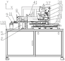
图1为带激光切割的芯片抽检机的主视图;Fig. 1 is the front view of the chip sampling machine with laser cutting;
图2为带激光切割的芯片抽检机的俯视图;Fig. 2 is the top view of the chip sampling machine with laser cutting;
图3为料盒机构的结构示意图;Fig. 3 is the structural representation of the material box mechanism;
图4为推料机构的结构示意图;Fig. 4 is the structural representation of pushing mechanism;
图5为取料机构和运输机构的结构示意图;Fig. 5 is the structural representation of the reclaiming mechanism and the transport mechanism;
图6为显微镜机构的结构示意图;6 is a schematic structural diagram of a microscope mechanism;
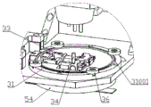
图7为显微镜的局部放大图。FIG. 7 is a partial enlarged view of the microscope.
具体实施方式Detailed ways
为了使本发明的目的、技术方案及优点更加清楚明白,以下结合附图及实施例,对本发明进行进一步详细说明。应当理解,此处所描述具体实施例仅仅用以解释本发明,并不用于限定本发明。In order to make the objectives, technical solutions and advantages of the present invention clearer, the present invention will be further described in detail below with reference to the accompanying drawings and embodiments. It should be understood that the specific embodiments described herein are only used to explain the present invention, but not to limit the present invention.
一种带激光切割功能的IC芯片光学抽检机,包括架体100和安装在架体100上的料盒机构、推料机构、取料机构、运输机构、显微镜机构、激光切割机构,显微镜机构和激光切割机构料并排设置;料盒机构的位置能上下、X方向、Y方向调节;推料机构能将料盒机构中的芯片条带从料盒机构中推出;取料机构能将被推料机构推出的芯片条带夹取到运输机构上;运输机构能将芯片条带运送到显微镜机构下观察或运送到激光切割机构下切割或打标。An IC chip optical sampling machine with laser cutting function, comprising a
盒机构包括X方向调节机构一、Y方向调节机构一、上下调节机构、料盒本体,X方向调节机构一能调节料盒本体在X方向上的位置;Y方向调节机构一能调节料盒本体在Y方向上的位置;上下调节机构能调节料盒本体的上下位置。上下调节机构包括固定在架体100上的料盒升降电机2,料盒升降电机2的输出端和丝杠一的一端连接,丝杠一的另一端和上下滑动板3连接,当料盒升降电机2转动时,上下滑动板3能在在竖直导轨一4上上下滑动;竖直导轨一4固定在固定板一5上,固定板一5固定在架体100上。X方向调节机构一包括安装在上下滑动板3上的气缸一,气缸一能驱动X向移动板6沿X方向移动。Y方向调节机构一包括安装在X向移动板6上的料盒固定基准面7,在料盒固定基准面7上安装有无杆气缸,无杆气缸能带动Y向移动面8沿Y方向移动,料盒本体固定在Y向移动面8上。The box mechanism includes an X-direction adjustment mechanism, a Y-direction adjustment mechanism, an up-down adjustment mechanism, and a material box body. The X-direction adjustment mechanism can adjust the position of the material box body in the X direction; the Y-direction adjustment mechanism can adjust the material box body. The position in the Y direction; the up and down adjustment mechanism can adjust the up and down position of the material box body. The up and down adjustment mechanism includes a material
推料机构包括固定在架体100上的支架、推针气缸9、推针装置,推针气缸9和推针装置安装在支架上,推针气缸9能带动推针装置移动推动芯片条带。推针装置包括安装在支架上的轨道二10、支架二11,支架二11在推针气缸9的作用下能在轨道二10上滑动;支架二11上安装有固定块12,固定块12与推针气缸9连接,推针13穿过固定块12与缓冲器52相连,缓冲器52固定在支架二11上;推料异常检测装置50能检测缓冲器52受到的压力。支架包括竖向支撑板14、Y向支撑板15、X向支撑板16,竖向支撑板14固定在架体100上,竖向支撑板14、Y向支撑板15通过连接板17连接,连接板17与竖向支撑板14的连接处为竖直腰形孔;Y向支撑板15与连接板17的连接处为Y方向的腰形孔;X向支撑板16安装在Y向支撑板15上,X向支撑板16与Y向支撑板15连接处为X方向的腰型孔。The pusher mechanism includes a bracket fixed on the
运输机构包括安装在架体100上的平台装置、安装在平台装置上的导轨装置,平台装置能在X方向和Y方向上移动;导轨装置的宽度可以根据芯片条带的宽度调节。平台装置包括平台18、平台X电机19、平台Y电机20,平台Y电机20固定安装在架体100上,平台Y电机20的输出端和Y丝杠21的一端连接,Y丝杠21的另一端穿过滑动件22;滑动件22上固定有平台X电机19,平台X电机19的输出端和X丝杆23的一端连接,X丝杆23的另一端和平台18连接。导轨装置包括固定导轨24、滑动导轨25、导轨电机26,固定导轨24和导轨电机26固定安装在平台18上,导轨丝杆的一端和导轨电机26连接,导轨丝杆的另一端穿过滑动导轨25;导轨电机26转动能带动滑动导轨25移动。取料机构安装在平台18上,取料机构包括取料机械手27、取料电机28,取料电机28的输出端和链条连接,取料机械手27和链条连接,链条转动能带动取料机械手27在取料导轨29上滑动。The transport mechanism includes a platform device mounted on the
显微镜机构包括显微镜30、安装在显微镜下的旋转台31、安装在旋转台31下的光源54,旋转台31能在旋转电机32的驱动下在水平面上旋转,旋转台31中安装有能在竖直方向上旋转的反光镜,显微镜30和旋转台31的竖直距离可以调节。反光镜包括反光镜一33和反光镜二34,镜片电机一能带动反光镜一33转动,镜片电机二能带动反光镜二34转动。旋转台31上开设有凹槽31001,皮带35套设在凹槽31001内和旋转电机32的输出端上。旋转台31上设有防止皮带35从凹槽31001中滑出的阻挡装置。阻挡装置包括橡胶垫36和固定橡胶垫36的螺丝,旋转台31上设有安装螺丝的螺纹孔。显微镜30的目镜处安装有CCD相机37,CCD相机37和监视画面显示器相连。显微镜30安装在升降机构38上,升降机构38能调节显微镜30与旋转台31的竖直距离;升降机构38安装在架体100上。激光切割机构包括振镜40和光纤激光器41,光纤激光器41安装在架体100上,振镜40和光纤激光器41连接。芯片抽检机还包括二维码扫描机构、与控制器连接的操作界面显示器。The microscope mechanism includes a
一种带激光切割功能的IC芯片光学抽检机的检验方法,包括以下步骤:An inspection method for an IC chip optical sampling machine with a laser cutting function, comprising the following steps:
步骤一:将芯片条带装入料盒本体,按下启动按钮,操作界面显示器提醒输入抽检层数;Step 1: Load the chip strip into the material box body, press the start button, and the operation interface display reminds to input the number of layers for sampling inspection;
步骤二:输入抽检层数,控制器控制升降电机2、气缸一、无杆气缸动作,让料盒本体被选择的抽检层对准推针13;Step 2: Input the number of sampling layers, the controller controls the movements of the lifting
步骤三:推针13将芯片料带推出;Step 3: Push
步骤四:控制器控制平台X电机19和平台Y电机20动作,让平台18移动到合适的位置,然后控制器控制取料电机28动作,让取料机械手27对准被推出的芯片条带;Step 4: the controller controls the action of the
步骤五:取料机械手27将芯片条带夹取放入到导轨装置内,期间控制器控制导轨电机动作,使导轨装置的宽度和芯片条带宽度相匹配;Step 5: The reclaiming
步骤六:二维码扫描机构读取芯片条带上的二维码;Step 6: The QR code scanning mechanism reads the QR code on the chip strip;
步骤七:控制器控制平台X电机19和平台Y电机20动作,将芯片条带运送到显微镜下;Step 7: The controller controls the movements of the
步骤八:观察Die是否正常;如果Die不正常,控制器控制平台X电机19和平台Y电机20动作,将芯片条带移动到激光机构下切割或打标,然后再移回显微镜下判断是否观察完毕;如果Die正常,直接判断是否观察完毕;Step 8: Observe whether the Die is normal; if the Die is not normal, the controller controls the action of the
步骤九:如果观察完毕,则执行步骤十;如果观察没有完毕,则执行步骤八;Step 9: If the observation is completed, go to step ten; if the observation is not completed, go to step eight;
步骤十:控制器控制平台X电机19、平台Y电机20、取料电机28动作,取料机械手27将芯片条带放回料盒本体;Step ten: the controller controls the action of the
步骤十一: 判断是否继续抽检其他层,如果要继续抽检其他层,则执行步骤二;如果不继续抽检其他层,则抽检结束。Step 11: Determine whether to continue sampling other layers. If you want to continue sampling other layers, go to
以上所述仅为本发明的较佳实施例而已,并不用以限制本发明,凡在本发明的精神和原则之内所作的任何修改、等同替换和改进等,均应包含在本发明的保护范围之内。The above descriptions are only preferred embodiments of the present invention and are not intended to limit the present invention. Any modifications, equivalent replacements and improvements made within the spirit and principles of the present invention shall be included in the protection of the present invention. within the range.
Claims (6)
Priority Applications (1)
| Application Number | Priority Date | Filing Date | Title |
|---|---|---|---|
| CN201810585880.1A CN109065469B (en) | 2018-06-08 | 2018-06-08 | Take laser cutting function's IC chip optics to take out machine of examining |
Applications Claiming Priority (1)
| Application Number | Priority Date | Filing Date | Title |
|---|---|---|---|
| CN201810585880.1A CN109065469B (en) | 2018-06-08 | 2018-06-08 | Take laser cutting function's IC chip optics to take out machine of examining |
Publications (2)
| Publication Number | Publication Date |
|---|---|
| CN109065469A CN109065469A (en) | 2018-12-21 |
| CN109065469B true CN109065469B (en) | 2020-10-16 |
Family
ID=64819989
Family Applications (1)
| Application Number | Title | Priority Date | Filing Date |
|---|---|---|---|
| CN201810585880.1A Active CN109065469B (en) | 2018-06-08 | 2018-06-08 | Take laser cutting function's IC chip optics to take out machine of examining |
Country Status (1)
| Country | Link |
|---|---|
| CN (1) | CN109065469B (en) |
Families Citing this family (2)
| Publication number | Priority date | Publication date | Assignee | Title |
|---|---|---|---|---|
| CN110837039A (en) * | 2019-11-28 | 2020-02-25 | 湖南凯通电子有限公司 | Resistance value measuring probe equipment |
| CN114260589A (en) * | 2022-01-24 | 2022-04-01 | 铜陵三佳山田科技股份有限公司 | Laser marking detection process and device for IC chip strip |
Citations (5)
| Publication number | Priority date | Publication date | Assignee | Title |
|---|---|---|---|---|
| CN201084716Y (en) * | 2007-09-20 | 2008-07-09 | 格兰达技术(深圳)有限公司 | Conveying device of IC bar laser marking machine |
| CN201084717Y (en) * | 2007-09-20 | 2008-07-09 | 格兰达技术(深圳)有限公司 | Feeding device of IC bar laser marking machine |
| CN102101217A (en) * | 2011-02-28 | 2011-06-22 | 深圳市大族激光科技股份有限公司 | Laser cutting device |
| CN104101377A (en) * | 2014-06-30 | 2014-10-15 | 格兰达技术(深圳)有限公司 | IC strip defective chip automatic detection and recording machine |
| CN205905562U (en) * | 2016-07-05 | 2017-01-25 | 宣利峰 | Laser marking machine |
-
2018
- 2018-06-08 CN CN201810585880.1A patent/CN109065469B/en active Active
Patent Citations (5)
| Publication number | Priority date | Publication date | Assignee | Title |
|---|---|---|---|---|
| CN201084716Y (en) * | 2007-09-20 | 2008-07-09 | 格兰达技术(深圳)有限公司 | Conveying device of IC bar laser marking machine |
| CN201084717Y (en) * | 2007-09-20 | 2008-07-09 | 格兰达技术(深圳)有限公司 | Feeding device of IC bar laser marking machine |
| CN102101217A (en) * | 2011-02-28 | 2011-06-22 | 深圳市大族激光科技股份有限公司 | Laser cutting device |
| CN104101377A (en) * | 2014-06-30 | 2014-10-15 | 格兰达技术(深圳)有限公司 | IC strip defective chip automatic detection and recording machine |
| CN205905562U (en) * | 2016-07-05 | 2017-01-25 | 宣利峰 | Laser marking machine |
Also Published As
| Publication number | Publication date |
|---|---|
| CN109065469A (en) | 2018-12-21 |
Similar Documents
| Publication | Publication Date | Title |
|---|---|---|
| CN109253702B (en) | PCB drilling quick overhaul method and equipment | |
| CN104483617B (en) | A kind of flip LED chips on-line measuring device | |
| TWI333544B (en) | Substrate inspection apparatus | |
| CN110581096B (en) | An LED chip optoelectronic and appearance integrated testing equipment | |
| CN214472864U (en) | Polaroid defect detection equipment and system | |
| CN204924972U (en) | Circuit board on -line measuring repair equipment | |
| CN203518947U (en) | Optical measurement equipment | |
| CN114544655B (en) | Automatic detection device for grid defects | |
| CN214622935U (en) | Probe card adjusting device | |
| JPH05166893A (en) | Probe card inspecting device | |
| CN209027768U (en) | A kind of OLED screen curtain feeding visual-alignment system | |
| CN111716362A (en) | Flip-over multi-axis robotic arm device and optical inspection equipment | |
| CN115753819A (en) | Wafer defect detection device and detection equipment thereof | |
| CN115254680A (en) | Automatic foreign matter detection equipment for display screen | |
| CN108291879B (en) | Substrate defect detection device and detection method using the same | |
| CN101673695B (en) | Bare die double-sided inspection equipment | |
| CN212059883U (en) | AOI inspection machine for silk screen printing plate | |
| CN206311047U (en) | A kind of product profile tolerance testing equipment | |
| CN104502828B (en) | A kind of flip LED chips online test method | |
| CN212821221U (en) | Visual inspection instrument for straight edge inspection of rear cover of mobile phone | |
| CN208271842U (en) | A kind of chip strip band fetching and sending devices for chip sampling observation machine | |
| CN211652024U (en) | Appearance inspection machine for finished products of backlight | |
| CN109065469A (en) | A kind of IC chip optics sampling observation machine of band laser cutting function | |
| CN218481432U (en) | High-precision detection device for surface defects of optical element | |
| CN208270841U (en) | A kind of microscope mechanisms of 360 degree of observations of energy |
Legal Events
| Date | Code | Title | Description |
|---|---|---|---|
| PB01 | Publication | ||
| PB01 | Publication | ||
| SE01 | Entry into force of request for substantive examination | ||
| SE01 | Entry into force of request for substantive examination | ||
| GR01 | Patent grant | ||
| GR01 | Patent grant | ||
| CP03 | Change of name, title or address |
Address after: 610000 floors 1-3, plant 9, No. 66, Antai seventh Road, high tech Zone, Chengdu, Sichuan Patentee after: Chengdu Laipu Technology Co.,Ltd. Address before: No. 11 high tech Zone Gaopeng road in Chengdu city of Sichuan Province in 610041 Patentee before: CHENGDU LAIPU TECHNOLOGY Co.,Ltd. |
|
| CP03 | Change of name, title or address | ||
| PE01 | Entry into force of the registration of the contract for pledge of patent right |
Denomination of invention: An IC chip optical sampling machine with laser cutting function Effective date of registration: 20220812 Granted publication date: 20201016 Pledgee: Chengdu SME financing Company Limited by Guarantee Pledgor: Chengdu Laipu Technology Co.,Ltd. Registration number: Y2022980012370 |
|
| PE01 | Entry into force of the registration of the contract for pledge of patent right | ||
| PC01 | Cancellation of the registration of the contract for pledge of patent right |
Date of cancellation: 20230508 Granted publication date: 20201016 Pledgee: Chengdu SME financing Company Limited by Guarantee Pledgor: Chengdu Laipu Technology Co.,Ltd. Registration number: Y2022980012370 |
|
| PC01 | Cancellation of the registration of the contract for pledge of patent right | ||
| PE01 | Entry into force of the registration of the contract for pledge of patent right |
Denomination of invention: An IC chip optical sampling machine with laser cutting function Granted publication date: 20201016 Pledgee: Chengdu SME financing Company Limited by Guarantee Pledgor: Chengdu Laipu Technology Co.,Ltd. Registration number: Y2024980001080 |
|
| PE01 | Entry into force of the registration of the contract for pledge of patent right | ||
| PC01 | Cancellation of the registration of the contract for pledge of patent right |
Granted publication date: 20201016 Pledgee: Chengdu SME financing Company Limited by Guarantee Pledgor: Chengdu Laipu Technology Co.,Ltd. Registration number: Y2024980001080 |
|
| PC01 | Cancellation of the registration of the contract for pledge of patent right |