CN107078385B - Antenna structure with dielectric loading - Google Patents
Antenna structure with dielectric loading Download PDFInfo
- Publication number
- CN107078385B CN107078385B CN201580016250.7A CN201580016250A CN107078385B CN 107078385 B CN107078385 B CN 107078385B CN 201580016250 A CN201580016250 A CN 201580016250A CN 107078385 B CN107078385 B CN 107078385B
- Authority
- CN
- China
- Prior art keywords
- conductive elements
- antenna
- conductive
- circuit board
- printed circuit
- Prior art date
- Legal status (The legal status is an assumption and is not a legal conclusion. Google has not performed a legal analysis and makes no representation as to the accuracy of the status listed.)
- Active
Links
Images

Classifications
-
- H—ELECTRICITY
- H01—ELECTRIC ELEMENTS
- H01Q—ANTENNAS, i.e. RADIO AERIALS
- H01Q9/00—Electrically-short antennas having dimensions not more than twice the operating wavelength and consisting of conductive active radiating elements
- H01Q9/04—Resonant antennas
- H01Q9/0485—Dielectric resonator antennas
-
- H—ELECTRICITY
- H01—ELECTRIC ELEMENTS
- H01Q—ANTENNAS, i.e. RADIO AERIALS
- H01Q1/00—Details of, or arrangements associated with, antennas
- H01Q1/36—Structural form of radiating elements, e.g. cone, spiral, umbrella; Particular materials used therewith
- H01Q1/38—Structural form of radiating elements, e.g. cone, spiral, umbrella; Particular materials used therewith formed by a conductive layer on an insulating support
-
- H—ELECTRICITY
- H01—ELECTRIC ELEMENTS
- H01Q—ANTENNAS, i.e. RADIO AERIALS
- H01Q1/00—Details of, or arrangements associated with, antennas
- H01Q1/48—Earthing means; Earth screens; Counterpoises
-
- H—ELECTRICITY
- H01—ELECTRIC ELEMENTS
- H01Q—ANTENNAS, i.e. RADIO AERIALS
- H01Q9/00—Electrically-short antennas having dimensions not more than twice the operating wavelength and consisting of conductive active radiating elements
- H01Q9/04—Resonant antennas
- H01Q9/0407—Substantially flat resonant element parallel to ground plane, e.g. patch antenna
- H01Q9/0421—Substantially flat resonant element parallel to ground plane, e.g. patch antenna with a shorting wall or a shorting pin at one end of the element
-
- H—ELECTRICITY
- H01—ELECTRIC ELEMENTS
- H01Q—ANTENNAS, i.e. RADIO AERIALS
- H01Q9/00—Electrically-short antennas having dimensions not more than twice the operating wavelength and consisting of conductive active radiating elements
- H01Q9/04—Resonant antennas
- H01Q9/30—Resonant antennas with feed to end of elongated active element, e.g. unipole
- H01Q9/42—Resonant antennas with feed to end of elongated active element, e.g. unipole with folded element, the folded parts being spaced apart a small fraction of the operating wavelength
-
- H—ELECTRICITY
- H01—ELECTRIC ELEMENTS
- H01Q—ANTENNAS, i.e. RADIO AERIALS
- H01Q1/00—Details of, or arrangements associated with, antennas
- H01Q1/12—Supports; Mounting means
- H01Q1/22—Supports; Mounting means by structural association with other equipment or articles
- H01Q1/24—Supports; Mounting means by structural association with other equipment or articles with receiving set
- H01Q1/241—Supports; Mounting means by structural association with other equipment or articles with receiving set used in mobile communications, e.g. GSM
- H01Q1/242—Supports; Mounting means by structural association with other equipment or articles with receiving set used in mobile communications, e.g. GSM specially adapted for hand-held use
- H01Q1/243—Supports; Mounting means by structural association with other equipment or articles with receiving set used in mobile communications, e.g. GSM specially adapted for hand-held use with built-in antennas
Abstract
An antenna structure (300) is described. The antenna structure (300) comprises a first set of conductive elements (305, 310) forming a first portion of the antenna structure (300), the first set of conductive elements (305, 310) being formed on a first layer of a multilayer printed circuit board; and a second set of conductive elements (306, 311) forming a second part of the antenna structure (300), the second set of conductive elements (306, 311) being formed parallel to the first set of conductive elements (305, 310) on a second layer of the multilayer printed circuit board, wherein the first and second layers are inner layers of the multilayer printed circuit board. An apparatus using the antenna structure (300) is also described.
Description
Cross Reference to Related Applications
This application claims the benefit of U.S. provisional application serial No. 61/970,432 filed on 26/3/2014, which is incorporated herein by reference in its entirety.
Technical Field
The present disclosure relates generally to antenna structures and, more particularly, to antenna structures including dielectric loading.
Background
This section is intended to introduce the reader to various aspects of art, which may be related to the embodiments described below. This discussion is believed to be helpful in providing the reader with background information to facilitate a better understanding of the various aspects of the present disclosure. Accordingly, it should be understood that these statements are to be read in this light.
Wireless communication networks exist in many communication systems today. Many communication devices used in systems include one or more antennas for interfacing to a network. These communication devices often include, but are not limited to, set-top boxes, gateways, cellular or wireless telephones, televisions, home computers, media content players, and the like. Further, many of these communication devices may include multiple interfaces for different types of networks. Thus, there may be one or more antennas on or in the communication device.
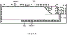
As communication devices continue to become smaller in size, the space allocated in the communication device for communication circuitry including the antenna(s) may also be reduced. The size or spacing required for the antenna may vary depending on a number of factors, including the choice of communication network and the type of antenna used. One particular operating scenario involves the use of inverted-f antennas in 2.4 gigahertz (GHz) home wireless networks. Fig. 1A-1C illustrate exemplary inverted-f antenna designs incorporated onto a printed circuit board located inside a communication device. Inverted-f antennas use top and bottom conductive copper layers of a multilayer printed circuit board. The conductive copper layers are bonded together with interlayer vias to form elements of the antenna.
Fig. 1A includes a conductive element 105. Element 105 operates with similar characteristics to a monopole antenna on the ground plane. One end of element 115 is connected to element 105 at a point a predetermined distance from one end of element 105. The other end of element 115 is connected to element 120. The element 120 is an interface point to circuitry, such as a connection point to communications circuitry. The length of element 105 is selected to be approximately a quarter wavelength of the operating frequency of the antenna. The distance from the end of element 105 to the connection point with element 115 is chosen such that the radiation resistance is as close as possible to the operating impedance or resistance for the communication circuit connected to element 120. The end of element 105 closest to element 115 is connected to one end of another conductive element 110. The other end of the element 110 is further connected to a conductive copper ground plane 125. The addition of element 110 is important to the structure of the inverted-f antenna. Since the antenna length is typically selected to be less than the full wavelength of the operating frequency for the antenna, the electrical interface for the antenna may operate electrically equivalent to a resistive element in series with a low value capacitive element. Element 110 operates electrically similar to adding an inductor in parallel with the remaining equivalent elements in the antenna. Thus, the element 110 reduces the effect of the equivalent series capacitance for the antenna. While the addition of series capacitance may be used to reduce the size of the antenna, the location and amount of additional series capacitance may also result in undesirable effects, including degradation of the antenna impedance or resistance and degradation of the antenna radiation pattern.
FIG. 1B includes mirror images of elements 105, 110, and 125, labeled 106, 111, and 126, respectively. Figure 1b does not include elements 115 and 120. The mirror image elements 105, 106, 110 and 111 in fig. 1A and 1A are connected together using vias 130 a-n. The mirror ground planes 125 and 126 in fig. 1A and 1B are connected together using vias 135 a-n. Vias 130 a-n and 135 a-n are spaced apart at a small fraction of the wavelength for the operating or resonant frequency of the antenna. Thus, a mirrored set of elements effectively acts as and operates as a single set of elements. The other ends of elements 150 and 106 are left disconnected or unconnected. These ends of elements 105 and 106 are also kept at a distance from conductive ground planes 125 and 126 so that any undesired or stray capacitances are kept to a minimum in order to have a negligible effect on the tuning or resonance frequency of the antenna.
FIG. 1C shows a three-dimensional view of the elements described with respect to FIGS. 1A and 1B.
Printed circuit board antennas, such as the inverted-f antenna described in fig. 1A-1C, additionally rely on characteristics associated with elements and materials surrounding the antenna in order to determine a relationship between antenna physical parameters and antenna electrical operating parameters. The physical parameters, including the size, thickness and length of the elements, along with the conductivity and dielectric constant of the material used with the antenna, determine the electrical operating frequency for the antenna. The antenna in fig. 1A-1C relies on a dielectric constant value associated with air (e.g., a dielectric constant value equal to one) as one of the physical parameters to determine the electrical parameter, and thus the physical parameter or dimension that constitutes the antenna. However, given the increasing constraints on space in devices, antennas with small physical parameters are desired, as previously described. Accordingly, there is a need to develop a printed circuit board antenna that is smaller in physical size than conventional printed circuit board antennas while maintaining the same or similar electrical operating parameters.
Disclosure of Invention
According to an aspect of the present disclosure, an antenna structure is described. The antenna structure includes a first set of conductive elements forming a first portion of the antenna structure formed on a first layer of the multilayer printed circuit board and a second set of conductive elements forming a second portion of the antenna structure formed parallel to the first set of conductive elements on a second layer of the multilayer printed circuit board, wherein the first and second layers are inner layers of the multilayer printed circuit board.
According to another aspect of the disclosure, a communication device is described. The communication device includes circuitry capable of at least one of transmitting and receiving signals and an antenna coupled to the circuitry. The antenna also includes a first set of conductive elements forming a first portion of the antenna structure on a first layer of the multi-layer printed circuit board and a second set of conductive elements forming a second portion of the antenna structure on a second layer of the multi-layer printed circuit board. The second set of conductive elements is formed in parallel with the first set of conductive elements, wherein the first and second layers are inner layers of a multilayer printed circuit board.
Drawings
These and other aspects, features and advantages of the present disclosure will be described or become apparent from the following detailed description of the preferred embodiments, which is to be read in connection with the accompanying drawings.
Fig. 1A is a diagram of a first view of an exemplary antenna;
fig. 1B is a diagram of a second view of an exemplary antenna;
fig. 1C is a diagram of a third view of an exemplary antenna;
fig. 2 is a block diagram of an exemplary communication device, in accordance with aspects of the present disclosure;
fig. 3 is a three-dimensional diagram of an exemplary antenna in accordance with aspects of the present disclosure;
fig. 4 is a side view of a printed circuit board structure associated with an exemplary antenna, in accordance with aspects of the present disclosure;
fig. 5 is a three-dimensional diagram of another exemplary antenna in accordance with aspects of the present disclosure;
fig. 6 is a diagram illustrating characteristics of an exemplary antenna in accordance with aspects of the present disclosure; and
fig. 7 is a flow diagram of an example process for manufacturing an antenna, in accordance with aspects of the present disclosure.
It should be understood that the drawing(s) is (are) for purposes of illustrating the concepts of the disclosure and is not necessarily the only possible configuration for illustrating the disclosure, as will be known to those skilled in the art.
Detailed Description
It should be understood that the elements shown in the fig. may be implemented in various forms of hardware, software or combinations thereof. Preferably, these elements are implemented in a combination of hardware and software on one or more appropriately programmed general-purpose devices, which may include a processor, memory and input/output interfaces. The phrase "coupled" is defined herein to mean connected directly to or indirectly through one or more intermediate components. Such intermediate components may include both hardware and software based components.
The present description illustrates the principles of the present disclosure. It will thus be appreciated that those skilled in the art will be able to devise various arrangements that, although not explicitly described or shown herein, embody the principles of the disclosure and are included within its scope.
All examples and conditional language recited herein are intended for pedagogical purposes to aid the reader in understanding the principles of the disclosure and the concepts contributed by the inventor to furthering the art, and are to be construed as being without limitation to such specifically recited examples and conditions.
Moreover, all statements herein reciting principles, aspects, and embodiments of the disclosure, as well as specific examples thereof, are intended to encompass both structural and functional equivalents thereof. Additionally, it is intended that such equivalents include both currently known equivalents as well as equivalents developed in the future, i.e., any elements developed that perform the same function, regardless of structure. For example, it will be appreciated by those skilled in the art that the diagrams presented herein represent conceptual views of illustrative circuitry and elements embodying the principles of the disclosure.
The functions of the various elements shown in the figures may be provided through the use of dedicated hardware as well as hardware capable of executing software in association with appropriate software. When provided by a processor, the functions may be provided by a single dedicated processor, by a single shared processor, or by a plurality of individual processors, some of which may be shared. Moreover, explicit use of the term "processor" or "controller" should not be construed to refer exclusively to hardware capable of executing software, and may implicitly include, without limitation, Digital Signal Processor (DSP) hardware, Read Only Memory (ROM) for storing software, Random Access Memory (RAM), and non-volatile storage.
The present disclosure is directed to problems associated with reducing the size of antennas used as part of communication circuits. As devices using antennas continue to shrink in size, efficient packaging and structures for components, including antennas, become more important. The antenna design may be limited by constraints and inherent tradeoffs between electrical operating parameters and physical characteristics. The present disclosure attempts to address at least some of these issues.
Embodiments of the present disclosure relate to an antenna that is printed onto or into a printed circuit board and utilizes printed circuit board material as part of a dielectric element associated with electrical properties for the antenna in order to reduce the physical size of the antenna. The antenna places conductive elements for the antenna in parallel on an inner layer of the circuit board, where the conductive elements are connected together using vias in the circuit board. The printed circuit board structure is described in connection with an antenna. In a printed circuit board structure, four copper surfaces or layers are sandwiched around three regions of material. The first and second layers are inner layers surrounded by material, while the third and fourth layers are top and bottom layers of the printed circuit board structure. Thus, the antenna structure is located within the material used for the printed circuit board.
Based on the structure used for the embodiment, the radiation field for the antenna passes symmetrically through the printed circuit board material before entering the air. The dielectric constant for printed circuit board material is greater than or equal to that for air. The higher dielectric constant produces a change in the relationship between the electrical and physical properties for the antenna, resulting in a reduced physical size for the antenna while maintaining a similar operating or resonant frequency. In addition, one end of the antenna may be capacitively coupled or loaded to the ground plane using the circuit board material as a dielectric in order to further reduce the size of the antenna.
Described herein are mechanisms for implementing one or more antennas in a communication device. In particular, the mechanism is described with respect to an inverted-f antenna. It is important to note that this mechanism may be suitable for use in other antenna designs, particularly those that may be conventionally designed to operate at frequencies associated with air dielectric interface designs implemented on printed circuit boards. The mechanism is further useful for antenna designs at frequencies below the frequency range for which microstrip or patch antennas can be switched practical (e.g., frequencies below 2.5 GHz). For example, the embodiments described below may be modified to operate with a dipole antenna included in or with the communication device with only minor modifications.
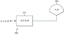
Turning now to fig. 2, a block diagram of an embodiment of a communication device 200 is shown, in accordance with aspects of the present disclosure. The communication device 200 may be used as part of a communication receiver, transmitter, and/or transceiver device, including but not limited to a handheld radio, a set-top box, a gateway, a modem, a cellular or wireless telephone, a television, a home computer, a tablet, and a media content player. The communication device 200 may include one or more interfaces to a wireless network, including but not limited to Wi-Fi, Institute of Electrical and Electronics Engineers (IEEE) standard 802.11, or other similar wireless communication protocols. It is important to note that the various components and interconnections necessary for the complete operation of the communication device 200, either as a stand-alone device or incorporated as part of another device, are not shown for the sake of simplicity, as the components not shown are well known to those skilled in the art.
The communication device 200 includes communication circuitry 210 that interfaces with other processing circuitry, such as a content source and/or a content playback device, not shown. The communication circuit 210 is connected to an antenna 220. The antenna 220 provides an interface to an electric wave to perform transmission and reception of signals to and from the communication apparatus 200.
The communication circuit 210 includes circuitry for improving the transmission and reception of signals interfaced to another device via the antenna 220 over a wireless network. The signal received from the antenna 220 may be amplified by a low noise amplifier and tuned by a set of filters, mixers, and oscillators. The tuned signal may be digitized and further demodulated and decoded. The decoded signal may be provided to other processing circuitry. In addition, communication circuit 210 generates, converts, and/or formats input signals (e.g., audio, video, or data signals) from other processing circuits for transmission through antenna 220. The communication circuit 210 may include a power amplifier for increasing the transmit signal level of signals transmitted from the communication device 200 over the wireless network. The amplification applied to signals received from the antenna 220 and the adjustment for amplification of signals transmitted by the antenna 220 may be controlled by circuitry in the communication circuit 210, or may be controlled by other processing circuitry.
The communication circuit 210 also includes an interface to send and receive data (e.g., audio and/or video signals) to other processing circuits (not shown). The communication circuit 200 further amplifies and processes the data to provide the data to the antenna 220 for transmission or to provide the data to other processing circuits. The communication circuit 210 may receive or transmit audio, video and/or data signals in analog or digital signal formats. In one embodiment, the communication circuit 210 has an ethernet interface for communicating data to other processing circuits and an Orthogonal Frequency Division Multiplexing (OFDM) interface for communicating with the antenna 220. The communication circuit 210 includes processing circuitry for converting signals between ethernet and OFDM formats.
It is important to note that more than one antenna 220 may be used in the communication device 200. The use of more than one antenna provides additional performance capabilities and control options. For example, in one embodiment, the first antenna may be oriented in a first orientation or axis and the second antenna oriented in a second orientation or axis. In another embodiment, the two antennas may be physically spaced apart at opposite ends of the communication device 200 or a larger device that includes the communication device 200. The use of multiple antennas as in the embodiments described herein allows for performance improvements such as orientation control, diversity transmission or reception, antenna steering (steering), and multiple-input multiple-output signal transmission and reception.
The communication device 200 in fig. 2 is primarily described as operating with a local wireless network, such as WiFi or IEEE 802.11. Those skilled in the art will recognize that other network standards incorporating a wireless physical interface may be used. For example, the communication device 200 may be readily used with a bluetooth network, a WiMax network, or any number of cellular telephone network protocols. Further, more than two networks may alternatively or simultaneously be used together.
Turning now to fig. 3, a three-dimensional diagram of an exemplary antenna 300 using aspects of the present disclosure is shown. The antenna 300 may be used as part of a communication device, such as the communication device 200 depicted in fig. 2. Further, the antenna 300 may be included in a larger multifunction device, such as but not limited to a handheld radio, a set-top box, a gateway, a modem, a cellular or wireless phone, a television, a home computer, a tablet, and a media content player.
The antenna 300 depicts an exemplary inverted-f antenna design incorporated into a printed circuit inside a communication device. Unlike previous printed circuit board antennas (such as the antenna described in fig. 1A-1C), the antenna 300 places conductive elements within the printed circuit board material and uses interlayer vias to form elements of the antenna.
It is physically impossible to immerse the entire near and far electromagnetic radiation fields into materials 345 and 350 that are part of a printed circuit board antenna, such as antenna 300. However, dielectric loading from antennas 345 and 350 present in the near radiated field has a significant and significant effect on the resonant frequency for antenna 300. In one embodiment, a thickness equal to.025 inches for both materials 345 and 350 reduces the resonant frequency for antenna 300 by about five percent compared to the case without materials 345 and 350. The physical length of elements 305 and 306 may be shortened due to dielectric loading in order to return the resonant frequency of antenna 300 to a desired resonant or operating frequency range. Antennas using the inner layer embodiment (such as antenna 300) for the conductive element take up less space and are physically smaller in size than similar structures using the outer layer embodiment (e.g., the antennas depicted in fig. 1A-1C).
Vias 330 a-n are shown as interlayer vias through material 340 along with vias 335 a-n, and also appear at the top and bottom after passing through materials 345 and 350. Vias 330 a-n may provide additional conductive surfaces for radiation of antenna 300. As previously described, the vias are spaced apart by a fraction of a wavelength (e.g., one tenth of a wavelength) for the operating frequency of the antenna 300. The small spacing causes the vias to function as if they were continuous and results in additional metal surface area and material thickness for the antenna 300. This additional metal surface area reduces resistive losses and improves antenna efficiency. However, the vias through materials 345 and 350 may further reduce the size or length of antenna 300. In an alternative embodiment, vias 330 a-n and/or vias 335 a-n may continue only through material 340 and not through materials 345 and 350, however, this alternative embodiment may also be used to reduce the benefits of the above-described additions. A through hole that passes only to connect the inner layers and does not pass to the top and bottom surfaces is called a blind hole.
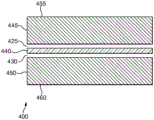
Turning now to fig. 4, a diagram of a printed circuit board structure 400 associated with an exemplary antenna is shown, in accordance with aspects of the present disclosure. In particular, the circuit board structure 400 will be described with respect to the antenna 300 depicted in fig. 3. The structure and manufacturing process for the printed circuit board will not be described in detail herein because it is well known to those skilled in the art.
Each conductive region 425, 430, 455, and 460 is typically very thin. The conductive material used in the conductive regions 425, 430, 455, and 460 is typically copper or a copper alloy. However, other conductive materials, such as silver, platinum or gold, may be used in pure or alloy form. The material regions 440, 445, and 450 may use common printed circuit board materials such as FR-4 and the like. The material used in material region 440 may be the same as or different from the material used for material regions 445 and 450. Additionally, material region 440 may be the same or different thickness than material regions 445 and 450. In one embodiment, the thickness for the conductive regions 425, 430, 455, and 460 is.0025 inches, the thickness for the material region 440 is.0125 inches, and the thickness for the material regions 445 and 450 is.025 inches. Other thicknesses may be used. It is important to note, however, that the operation of antenna 300 depends on the value of the dielectric constant of the material used in material regions 445 and 450 as well as the thickness of the material. The improvement achieved by the principles of the present embodiment will be affected by the thickness of the material in material regions 445 and 450 and the value of the dielectric constant for that material.
Further, circuit board structure 400 illustrates a multi-layer board, referred to as a four-layer board, that includes two inner layers and two outer layers. Other embodiments may utilize more layers. For example, in another embodiment, the circuit board structure may use an eight-layer printed circuit board that includes seven material regions and six conductive regions. To benefit most from the principles of this disclosure, the innermost layer or conductive region of the multilayer board should be used for the conductive elements of the antenna structure.
Turning now to fig. 5, a three-dimensional diagram of another exemplary antenna 500 using aspects of the present disclosure is shown. The antenna 500 may be used as part of a communication device, such as the communication device 200 depicted in fig. 2. Further, the antenna 500 may be included in a larger multifunction device, such as but not limited to a handheld radio, a set-top box, a gateway, a modem, a cellular or wireless phone, a television, a home computer, a tablet, and a media content player. Except as described herein, the elements of antenna 500 are positioned and function in a similar manner as similarly numbered elements described with respect to antenna 300 depicted in fig. 3.
The antenna 500 also includes a portion of ground plane 525 and ground plane 526, labeled 527 and 528, respectively. Portions 527 and 528 are located in close proximity to the open or unconnected ends of elements 505 and 506, respectively. Configurations in antenna 500 capacitively load or capacitively couple the ends of elements 505 and 506 to ground at portions 527 and 528. As mentioned above, capacitive loading is generally undesirable for operation of the antenna. However, the configuration in antenna 500 creates a capacitive coupling that is concentrated to the ends of elements 505 and 506 and dielectrically loaded through materials 540, 545, and 550.
The additional capacitive coupling further reduces the operating or resonant frequency for the antenna 500. Thus, the size of the antenna 500 may be reduced, primarily by reducing the length of the elements 505 and 506. In one embodiment, the length of elements 505 and 506 is reduced to 10.4 millimeters (mm) compared to the original length of 16.6 mm. In addition, the closer proximity of the ground planes 527 and 528 reduces the overall length of the antenna 500 from 26.6 mm to 12.3 mm.
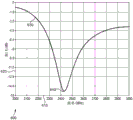
Fig. 6 illustrates a graph 600 of electrical characteristics of the antenna 500 according to aspects of the present disclosure. Graph 600 represents a scalar value for return loss of antenna 500 versus frequency measured at the antenna electrical terminals (e.g., element 520). Graph 600 includes an x-axis 610 that shows frequency in megahertz (MHz). Graph 600 also includes a y-axis 620 showing return loss in decibels (dB) shown as (S1, 1). Line 630 shows the value versus the contrast frequency for the return loss of the antenna 500. Point 640 shows a minimum value for return loss representing the point of optimal impedance matching between the antenna 500 and the expected circuit impedance at element 520.
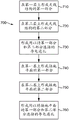
Turning now to fig. 7, a flow diagram of an exemplary process 700 for manufacturing an antenna is shown, in accordance with aspects of the present disclosure. Process 700 may be incorporated as part of a process for manufacturing an antenna, such as antenna 300 previously described in fig. 3 or antenna 300 previously described in fig. 5. The process 700 may also be incorporated as part of a process for manufacturing a communication device, such as the communication device 200 described in fig. 2. Process 700 may also rely on certain manufacturing techniques and materials, including but not limited to those described in fig. 4. Specific details regarding certain manufacturing techniques required to manufacture the antenna and/or device will not be described further herein as they are well known to those skilled in the art.
Process 700 forms an antenna using two internal layers of a printed circuit board as part of the manufacturing process. The inner layers are connected by a plurality of conductive vias or elements also formed during the manufacturing process. In one embodiment, the antenna formed by process 700 is an inverted-F antenna intended to operate at frequencies of 2.5 GHz or less.
At step 710, a first portion of an antenna structure is formed on a first layer of a multi-layer printed circuit board using a first set of conductive elements. At step 720, a second portion of the antenna structure is formed on a second layer of the multi-layer printed circuit board using a second set of conductive elements. It is important to note that the first and second sets of conductive elements are formed such that the second set of conductive elements is parallel to the first set of conductive elements. Next, at step 730, a plurality of conductive vias or elements are formed to connect the first set of conductive elements to the second set of conductive elements formed at steps 710 and 720. It is important to note that other attachment structures may be used at step 730, or attachment step 730 may be combined as an inherent part of step 710 and/or step 720.
In some embodiments, process 700 may continue to form additional structures related to a ground plane for the antenna. The ground plane may reduce the size of the antenna structure when a portion of the first conductive ground plane and a portion of the second conductive ground plane are capacitively coupled to a portion of the first set of conductive elements and a portion of the second set of conductive elements.
At step 740, a first conductive ground plane is formed on a first layer of the multi-layer printed circuit board. At step 750, a second conductive ground plane is formed on a second layer of the multi-layer printed circuit board such that the second conductive ground plane is parallel to the first conductive ground plane. Finally, at step 760, a plurality of conductive vias or elements connect the first and second conductive ground planes together. As with previous step 730, the connection at step 760 may be accomplished by mechanisms other than through-hole connections, or step 730 may be incorporated into steps 740 and 750.
Embodiments herein describe an antenna that is printed onto or into a printed circuit board and utilizes printed circuit board material as part of a dielectric element associated with electrical properties for the antenna in order to reduce the physical size of the antenna. The antenna is described as being used as part of a communication device. The antenna places conductive elements for the antenna on the inner layers of the circuit board, where the conductive elements are connected together using vias in the circuit board.
The configuration described in this embodiment effectively places a dielectric material around the entire conductive surface of the antenna. Thus, the radiation field for the antenna passes symmetrically through the printed circuit board material before entering the air. The dielectric constant for printed circuit board material is greater than the dielectric constant for air. The higher dielectric constant produces a change in the relationship between the electrical and physical properties for the antenna, resulting in a reduced physical size for the antenna while maintaining a similar operating or resonant frequency. In addition, one end of the antenna may be capacitively coupled or loaded to the ground plane using the circuit board material as a dielectric in order to further reduce the size of the antenna.
Although the embodiments which incorporate the teachings of the present disclosure have been shown and described in detail herein, those skilled in the art can readily devise many other varied embodiments that still incorporate these teachings. Having described preferred embodiments of the antenna using dielectric loading (which are intended to be illustrative and not limiting), it is noted that modifications and variations can be made by persons skilled in the art in light of the above teachings. It is therefore to be understood that changes may be made in the embodiments of the disclosure disclosed which are within the scope of the disclosure as outlined by the appended claims.
Claims (24)
1. An antenna structure comprising:
a multilayer printed circuit board having first (425) and second inner layers (430) separated by a first material region (440) and third (455) and fourth outer layers (460) separated from the first and second inner layers by second (445) and third (450) material regions, respectively;
a first set of conductive elements (305, 505, 310, 510, 315, 515) forming a first portion of the antenna structure formed on the first inner layer and comprising a first radiator arm (305, 505), a first shorting arm (310, 510), and a feeder arm (315, 515);
a second set of conductive elements (306, 506, 311, 511) forming a second portion of the antenna structure, the second portion being formed parallel to the first set of conductive elements (305, 505, 310, 510, 315, 515) on a second inner layer and comprising a second radiator arm (306, 506) and a second shorting arm (311, 511), the first and second sets of conductive elements being configured to act as an inverted-f antenna, wherein the first radiator arm (305, 505) and the second radiator arm (306, 506) are connected together using a plurality of conductive vias, and wherein the first shorting arm (310, 510) and the second shorting arm (311, 511) are connected together using a plurality of conductive vias;
a first conductive ground plane (325, 525) formed on a first layer of the multilayer printed circuit board; and
a second conductive ground plane (326, 526) formed parallel to the first conductive ground plane (325, 525) on a second layer of the multilayer printed circuit board, the second conductive ground plane (326, 526) and the first conductive ground plane (325, 525) being connected together using conductive vias.
2. The antenna structure of claim 1, wherein a portion of the first conductive ground plane (325) and a portion of the second conductive ground plane (326) are capacitively coupled to a portion of the first set of conductive elements (305, 310) and a portion of the second set of conductive elements (306, 311).
3. The antenna structure according to claim 1, wherein the second set of conductive elements (306, 311) is formed as a mirror image of the first set of conductive elements (305, 310).
4. The antenna structure according to claim 1, wherein the first set of conductive elements (305, 310) and the second set of conductive elements (306, 311) are integrated within a material used as a base material for a multilayer printed circuit board.
5. The antenna structure according to claim 4, wherein the base material for the printed circuit board has a dielectric constant value greater than air.
6. The antenna structure according to claim 5, wherein the first set of conductive elements (305, 310) and the second set of conductive elements (306, 311) integrated within the material used as a base material for the multilayer printed circuit board reduce the physical dimensions of the antenna structure for a given frequency of electrical operation.
7. The antenna structure of claim 2, wherein the capacitive coupling reduces the physical size of the antenna structure for a given frequency of electrical operation.
8. The antenna structure of claim 1, wherein the antenna structure (300) is used at an electrical frequency of less than or equal to 2.5 gigahertz.
9. A communication device, comprising:
a circuit (210) capable of at least one of transmitting and receiving a signal; and
the antenna structure of claim 1.
10. The communication device of claim 9, wherein a portion of the first conductive ground plane (325) and a portion of the second conductive ground plane (326) are capacitively coupled to a portion of the first set of conductive elements (305, 310) and a portion of the second set of conductive elements (306, 311).
11. The communication device of claim 9, wherein the second set of conductive elements is formed as a mirror image of the first set of conductive elements.
12. The communication device of claim 9, wherein the first set of conductive elements and the second set of conductive elements are integrated within a material used as a base material for a printed circuit board.
13. The communication device of claim 12, wherein the base material for the printed circuit board has a dielectric constant value greater than air.
14. The communication device of claim 13, wherein the first and second sets of conductive elements integrated within a material used as a base material for a multilayer printed circuit board reduce the physical size of the antenna (220) for a given frequency of electrical operation.
15. The communication device of claim 10, wherein the capacitive coupling reduces a physical size of the antenna (220) for a given frequency of electrical operation.
16. The communication device of claim 9, wherein the antenna (220) is used at an electrical frequency less than or equal to 2.5 gigahertz.
17. A method for manufacturing an antenna structure, comprising:
forming a first portion of an antenna structure on a first inner layer of a multilayer printed circuit board using a first set of conductive elements comprising a first radiator arm (305, 505), a first shorting arm (310, 510), and a feeder arm (315, 515);
forming a second portion of the antenna structure on a second inner layer of the multilayer printed circuit board using a second set of conductive elements such that the second set of conductive elements is parallel to the first set of conductive elements, the second set of conductive elements including a second radiator arm (306, 506) and a second shorting arm (311, 511), the first and second sets of conductive elements configured to act as an inverted-f antenna;
forming a plurality of conductive vias to connect the first radiator arm (305, 505) and the second radiator arm (306, 506) together and to connect the first shorting arm (310, 510) and the second shorting arm (311, 511) together;
separating the first and second inner layers with a region of material disposed therebetween;
placing an outer material region around the first and second inner layers;
forming a first conductive ground plane (325, 525) on a first layer of a multilayer printed circuit board;
forming a second conductive ground plane (326, 526) on a second layer of the multi-layer printed circuit board such that the second conductive ground plane is parallel to the first conductive ground plane; and
a plurality of conductive vias are formed to connect the first and second conductive ground planes together.
18. The method of claim 17, wherein a portion of the first conductive ground plane and a portion of the second conductive ground plane are capacitively coupled to a portion of the first set of conductive elements and a portion of the second set of conductive elements.
19. The method of claim 17, wherein the second set of conductive elements is formed as a mirror image of the first set of conductive elements.
20. The method of claim 17, wherein the first set of conductive elements and the second set of conductive elements are integrated within a material used as a base material for a multilayer printed circuit board.
21. The method of claim 20, wherein the base material for the printed circuit board has a dielectric constant value greater than air.
22. The method of claim 21, wherein the first and second sets of conductive elements integrated within a material used as a base material for a multilayer printed circuit board reduce the physical size of the antenna structure for a given frequency of electrical operation.
23. The method of claim 18, wherein the capacitive coupling reduces a physical size of the antenna structure for a given frequency of electrical operation.
24. The method of claim 17, wherein the antenna structure is used at an electrical frequency less than or equal to 2.5 gigahertz.
Applications Claiming Priority (3)
| Application Number | Priority Date | Filing Date | Title |
|---|---|---|---|
| US201461970432P | 2014-03-26 | 2014-03-26 | |
| US61/970432 | 2014-03-26 | ||
| PCT/US2015/021712 WO2015148298A1 (en) | 2014-03-26 | 2015-03-20 | An antenna structure with dielectric loading |
Publications (2)
| Publication Number | Publication Date |
|---|---|
| CN107078385A CN107078385A (en) | 2017-08-18 |
| CN107078385B true CN107078385B (en) | 2020-02-14 |
Family
ID=52808195
Family Applications (1)
| Application Number | Title | Priority Date | Filing Date |
|---|---|---|---|
| CN201580016250.7A Active CN107078385B (en) | 2014-03-26 | 2015-03-20 | Antenna structure with dielectric loading |
Country Status (6)
| Country | Link |
|---|---|
| US (1) | US10326206B2 (en) |
| EP (1) | EP3123559B1 (en) |
| JP (1) | JP6621418B2 (en) |
| KR (1) | KR20160137550A (en) |
| CN (1) | CN107078385B (en) |
| WO (1) | WO2015148298A1 (en) |
Families Citing this family (7)
| Publication number | Priority date | Publication date | Assignee | Title |
|---|---|---|---|---|
| AU2018230992B2 (en) * | 2017-03-07 | 2023-07-27 | Smith & Nephew, Inc. | Reduced pressure therapy systems and methods including an antenna |
| ES2737879A1 (en) * | 2018-07-16 | 2020-01-16 | Verisure Sarl | Printed circuit board for the control unit of an alarm system (Machine-translation by Google Translate, not legally binding) |
| DE102018212319A1 (en) * | 2018-07-24 | 2020-01-30 | BSH Hausgeräte GmbH | PCB antenna |
| DE102019205556A1 (en) * | 2019-04-17 | 2020-10-22 | BSH Hausgeräte GmbH | PCB antenna |
| CN110308336B (en) * | 2019-07-04 | 2021-05-07 | 中国人民解放军63660部队 | Dielectric loaded D-dot electric field measuring sensor |
| CN111430897A (en) * | 2020-03-05 | 2020-07-17 | 泰凌微电子(上海)有限公司 | Antenna structure, communication device and method for forming antenna structure |
| US20210307672A1 (en) | 2020-04-05 | 2021-10-07 | Epitel, Inc. | Eeg recording and analysis |
Citations (3)
| Publication number | Priority date | Publication date | Assignee | Title |
|---|---|---|---|---|
| JPH09270618A (en) * | 1996-03-29 | 1997-10-14 | Mitsubishi Electric Corp | Antenna system |
| CN1341980A (en) * | 2000-08-31 | 2002-03-27 | 夏普公司 | Image antenna and radio communication device with said antenna |
| US7796085B2 (en) * | 2005-10-28 | 2010-09-14 | Shinko Electric Industries Co., Ltd. | Antenna and wiring board |
Family Cites Families (14)
| Publication number | Priority date | Publication date | Assignee | Title |
|---|---|---|---|---|
| JP3482089B2 (en) * | 1996-12-25 | 2003-12-22 | シャープ株式会社 | Frequency switching inverted F antenna |
| EP1239539A3 (en) * | 2001-03-02 | 2003-11-05 | Nokia Corporation | Antenna |
| JP2004201278A (en) * | 2002-12-06 | 2004-07-15 | Sharp Corp | Pattern antenna |
| US7095382B2 (en) * | 2003-11-24 | 2006-08-22 | Sandbridge Technologies, Inc. | Modified printed dipole antennas for wireless multi-band communications systems |
| US7183994B2 (en) * | 2004-11-22 | 2007-02-27 | Wj Communications, Inc. | Compact antenna with directed radiation pattern |
| KR101459768B1 (en) | 2008-04-08 | 2014-11-12 | 엘지이노텍 주식회사 | Antenna |
| KR101039697B1 (en) | 2008-12-26 | 2011-06-08 | 전자부품연구원 | Printed circuit board and embeding antenna device having the same |
| US8044877B2 (en) * | 2009-05-15 | 2011-10-25 | Cheng Uei Precision Industry Co., Ltd. | Antenna |
| EP2348578A1 (en) | 2010-01-20 | 2011-07-27 | Insight sip sas | Improved antenna-in-package structure |
| EP2599366A4 (en) | 2010-07-28 | 2014-12-24 | Nokia Corp | Telecommunication apparatus and associated methods |
| US8611953B2 (en) * | 2010-12-07 | 2013-12-17 | M/A-Com Technology Solutions Holdings, Inc. | Integrated GPS receiver and cellular transceiver module for automotive bus applications |
| TWM421612U (en) * | 2011-06-14 | 2012-01-21 | Unictron Technologies Corp | Curly broadband antenna apparatus |
| WO2013011702A1 (en) * | 2011-07-20 | 2013-01-24 | 株式会社フジクラ | Antenna and wireless tag |
| JP6077207B2 (en) * | 2011-10-18 | 2017-02-08 | 富士通コンポーネント株式会社 | Memory card |
-
2015
- 2015-03-20 US US15/124,689 patent/US10326206B2/en active Active
- 2015-03-20 EP EP15714141.7A patent/EP3123559B1/en active Active
- 2015-03-20 WO PCT/US2015/021712 patent/WO2015148298A1/en active Application Filing
- 2015-03-20 KR KR1020167026572A patent/KR20160137550A/en unknown
- 2015-03-20 JP JP2016559232A patent/JP6621418B2/en not_active Expired - Fee Related
- 2015-03-20 CN CN201580016250.7A patent/CN107078385B/en active Active
Patent Citations (3)
| Publication number | Priority date | Publication date | Assignee | Title |
|---|---|---|---|---|
| JPH09270618A (en) * | 1996-03-29 | 1997-10-14 | Mitsubishi Electric Corp | Antenna system |
| CN1341980A (en) * | 2000-08-31 | 2002-03-27 | 夏普公司 | Image antenna and radio communication device with said antenna |
| US7796085B2 (en) * | 2005-10-28 | 2010-09-14 | Shinko Electric Industries Co., Ltd. | Antenna and wiring board |
Also Published As
| Publication number | Publication date |
|---|---|
| WO2015148298A1 (en) | 2015-10-01 |
| EP3123559A1 (en) | 2017-02-01 |
| CN107078385A (en) | 2017-08-18 |
| KR20160137550A (en) | 2016-11-30 |
| EP3123559B1 (en) | 2020-01-01 |
| US10326206B2 (en) | 2019-06-18 |
| JP6621418B2 (en) | 2019-12-18 |
| JP2017514368A (en) | 2017-06-01 |
| US20170085000A1 (en) | 2017-03-23 |
Similar Documents
| Publication | Publication Date | Title |
|---|---|---|
| CN107078385B (en) | Antenna structure with dielectric loading | |
| JP4343655B2 (en) | antenna | |
| CN110178267B (en) | Antenna device and communication device | |
| US8581799B2 (en) | Ground radiation antenna | |
| JP5669043B2 (en) | Post-wall waveguide antenna and antenna module | |
| JP2007281990A (en) | Antenna device and wireless communication instrument using the same | |
| US20100309087A1 (en) | Chip antenna device | |
| US8026855B2 (en) | Radio apparatus and antenna thereof | |
| US20110285599A1 (en) | Antenna | |
| Luo et al. | A differential‐fed Yagi–Uda antenna with enhanced bandwidth via addition of parasitic resonator | |
| JP5213039B2 (en) | Single-sided radiation antenna | |
| US20110221638A1 (en) | Internal lc antenna for wireless communication device | |
| US8604998B2 (en) | Ground radiation antenna | |
| US20150009093A1 (en) | Antenna apparatus and portable wireless device equipped with the same | |
| JP6014071B2 (en) | Communication device and antenna device | |
| US8970443B2 (en) | Compact balanced embedded antenna | |
| KR20090061585A (en) | Antenna device | |
| US20230208021A1 (en) | Devices with Radiating Systems Proximate to Conductive Bodies | |
| WO2019215970A1 (en) | Filter circuit and communication device | |
| CN109792104B (en) | Antenna device, antenna assembly and communication device | |
| EP2267834A1 (en) | Efficient integrated miniature antenna structure for multi-GHz wireless applications | |
| EP3787113A1 (en) | Antenna module and terminal | |
| CN107994329B (en) | Compact 4G LTE MIMO and GPS three-in-one antenna | |
| CN111602289B (en) | Antenna and communication apparatus | |
| EP4307481A1 (en) | Antenna |
Legal Events
| Date | Code | Title | Description |
|---|---|---|---|
| PB01 | Publication | ||
| PB01 | Publication | ||
| SE01 | Entry into force of request for substantive examination | ||
| SE01 | Entry into force of request for substantive examination | ||
| GR01 | Patent grant | ||
| GR01 | Patent grant |