CN106269451B - Piezoelectric transducer using micro-dome array - Google Patents
Piezoelectric transducer using micro-dome array Download PDFInfo
- Publication number
- CN106269451B CN106269451B CN201610701812.8A CN201610701812A CN106269451B CN 106269451 B CN106269451 B CN 106269451B CN 201610701812 A CN201610701812 A CN 201610701812A CN 106269451 B CN106269451 B CN 106269451B
- Authority
- CN
- China
- Prior art keywords
- piezoelectric
- vibrating
- reference electrode
- piezoelectric element
- drive
- Prior art date
- Legal status (The legal status is an assumption and is not a legal conclusion. Google has not performed a legal analysis and makes no representation as to the accuracy of the status listed.)
- Active
Links
- 239000000758 substrate Substances 0.000 claims abstract description 65
- 229910052751 metal Inorganic materials 0.000 claims description 18
- 239000002184 metal Substances 0.000 claims description 18
- 239000012528 membrane Substances 0.000 claims description 13
- 230000004044 response Effects 0.000 claims description 13
- 230000005496 eutectics Effects 0.000 claims description 6
- 230000002093 peripheral effect Effects 0.000 claims description 4
- 238000012545 processing Methods 0.000 abstract description 6
- 239000010408 film Substances 0.000 description 51
- 239000000463 material Substances 0.000 description 26
- 229910052451 lead zirconate titanate Inorganic materials 0.000 description 17
- 238000000034 method Methods 0.000 description 13
- 230000007704 transition Effects 0.000 description 13
- 238000003491 array Methods 0.000 description 11
- 238000000151 deposition Methods 0.000 description 11
- 230000001681 protective effect Effects 0.000 description 11
- 230000010287 polarization Effects 0.000 description 10
- 238000004544 sputter deposition Methods 0.000 description 10
- 230000008859 change Effects 0.000 description 9
- 238000004519 manufacturing process Methods 0.000 description 9
- 238000006073 displacement reaction Methods 0.000 description 8
- 238000003384 imaging method Methods 0.000 description 8
- 239000002245 particle Substances 0.000 description 8
- 230000008569 process Effects 0.000 description 8
- 239000004020 conductor Substances 0.000 description 7
- 230000006870 function Effects 0.000 description 7
- 239000004065 semiconductor Substances 0.000 description 6
- 238000013461 design Methods 0.000 description 5
- 230000005684 electric field Effects 0.000 description 5
- 229910052741 iridium Inorganic materials 0.000 description 5
- 230000001902 propagating effect Effects 0.000 description 5
- 238000002604 ultrasonography Methods 0.000 description 5
- 238000005530 etching Methods 0.000 description 4
- 238000001746 injection moulding Methods 0.000 description 4
- -1 IrO2 Chemical class 0.000 description 3
- ROXBGBWUWZTYLZ-UHFFFAOYSA-N [6-[[10-formyl-5,14-dihydroxy-13-methyl-17-(5-oxo-2h-furan-3-yl)-2,3,4,6,7,8,9,11,12,15,16,17-dodecahydro-1h-cyclopenta[a]phenanthren-3-yl]oxy]-4-methoxy-2-methyloxan-3-yl] 4-[2-(4-azido-3-iodophenyl)ethylamino]-4-oxobutanoate Chemical compound O1C(C)C(OC(=O)CCC(=O)NCCC=2C=C(I)C(N=[N+]=[N-])=CC=2)C(OC)CC1OC(CC1(O)CCC2C3(O)CC4)CCC1(C=O)C2CCC3(C)C4C1=CC(=O)OC1 ROXBGBWUWZTYLZ-UHFFFAOYSA-N 0.000 description 3
- 230000008901 benefit Effects 0.000 description 3
- 238000005520 cutting process Methods 0.000 description 3
- 230000008021 deposition Effects 0.000 description 3
- 229910052737 gold Inorganic materials 0.000 description 3
- 150000002739 metals Chemical class 0.000 description 3
- 229910052697 platinum Inorganic materials 0.000 description 3
- 230000000284 resting effect Effects 0.000 description 3
- 239000010409 thin film Substances 0.000 description 3
- 210000001519 tissue Anatomy 0.000 description 3
- 229910002711 AuNi Inorganic materials 0.000 description 2
- 229910021543 Nickel dioxide Inorganic materials 0.000 description 2
- 229910019020 PtO2 Inorganic materials 0.000 description 2
- 230000001154 acute effect Effects 0.000 description 2
- 229910045601 alloy Inorganic materials 0.000 description 2
- 239000000956 alloy Substances 0.000 description 2
- 239000000919 ceramic Substances 0.000 description 2
- 239000011248 coating agent Substances 0.000 description 2
- 238000000576 coating method Methods 0.000 description 2
- 239000002131 composite material Substances 0.000 description 2
- 238000011109 contamination Methods 0.000 description 2
- 238000005260 corrosion Methods 0.000 description 2
- 230000007797 corrosion Effects 0.000 description 2
- 230000008878 coupling Effects 0.000 description 2
- 238000010168 coupling process Methods 0.000 description 2
- 238000005859 coupling reaction Methods 0.000 description 2
- 238000010586 diagram Methods 0.000 description 2
- 238000005516 engineering process Methods 0.000 description 2
- GKOZUEZYRPOHIO-UHFFFAOYSA-N iridium atom Chemical compound [Ir] GKOZUEZYRPOHIO-UHFFFAOYSA-N 0.000 description 2
- HTXDPTMKBJXEOW-UHFFFAOYSA-N iridium(IV) oxide Inorganic materials O=[Ir]=O HTXDPTMKBJXEOW-UHFFFAOYSA-N 0.000 description 2
- 238000001755 magnetron sputter deposition Methods 0.000 description 2
- 229910044991 metal oxide Inorganic materials 0.000 description 2
- 150000004706 metal oxides Chemical class 0.000 description 2
- 238000000623 plasma-assisted chemical vapour deposition Methods 0.000 description 2
- 230000005855 radiation Effects 0.000 description 2
- 230000009467 reduction Effects 0.000 description 2
- 230000035945 sensitivity Effects 0.000 description 2
- 230000001225 therapeutic effect Effects 0.000 description 2
- 229910052718 tin Inorganic materials 0.000 description 2
- XLYOFNOQVPJJNP-UHFFFAOYSA-N water Substances O XLYOFNOQVPJJNP-UHFFFAOYSA-N 0.000 description 2
- XUIMIQQOPSSXEZ-UHFFFAOYSA-N Silicon Chemical compound [Si] XUIMIQQOPSSXEZ-UHFFFAOYSA-N 0.000 description 1
- 238000000231 atomic layer deposition Methods 0.000 description 1
- 238000005452 bending Methods 0.000 description 1
- 210000004204 blood vessel Anatomy 0.000 description 1
- 210000000988 bone and bone Anatomy 0.000 description 1
- 210000004556 brain Anatomy 0.000 description 1
- 238000005229 chemical vapour deposition Methods 0.000 description 1
- 238000010276 construction Methods 0.000 description 1
- 238000007796 conventional method Methods 0.000 description 1
- 239000013078 crystal Substances 0.000 description 1
- 238000013144 data compression Methods 0.000 description 1
- 230000007547 defect Effects 0.000 description 1
- 230000032798 delamination Effects 0.000 description 1
- 230000001934 delay Effects 0.000 description 1
- 230000001419 dependent effect Effects 0.000 description 1
- 238000001514 detection method Methods 0.000 description 1
- 239000000428 dust Substances 0.000 description 1
- 238000002592 echocardiography Methods 0.000 description 1
- 210000001508 eye Anatomy 0.000 description 1
- 238000000227 grinding Methods 0.000 description 1
- 238000010438 heat treatment Methods 0.000 description 1
- 238000002347 injection Methods 0.000 description 1
- 239000007924 injection Substances 0.000 description 1
- 238000003780 insertion Methods 0.000 description 1
- 230000037431 insertion Effects 0.000 description 1
- 230000010354 integration Effects 0.000 description 1
- 238000002608 intravascular ultrasound Methods 0.000 description 1
- 238000007735 ion beam assisted deposition Methods 0.000 description 1
- 238000001659 ion-beam spectroscopy Methods 0.000 description 1
- HFGPZNIAWCZYJU-UHFFFAOYSA-N lead zirconate titanate Chemical compound [O-2].[O-2].[O-2].[O-2].[O-2].[Ti+4].[Zr+4].[Pb+2] HFGPZNIAWCZYJU-UHFFFAOYSA-N 0.000 description 1
- 238000012986 modification Methods 0.000 description 1
- 230000004048 modification Effects 0.000 description 1
- 229910052759 nickel Inorganic materials 0.000 description 1
- 238000004806 packaging method and process Methods 0.000 description 1
- 238000000059 patterning Methods 0.000 description 1
- 238000005240 physical vapour deposition Methods 0.000 description 1
- 238000001020 plasma etching Methods 0.000 description 1
- 239000011253 protective coating Substances 0.000 description 1
- 238000001552 radio frequency sputter deposition Methods 0.000 description 1
- 238000005546 reactive sputtering Methods 0.000 description 1
- 238000001878 scanning electron micrograph Methods 0.000 description 1
- 229910052710 silicon Inorganic materials 0.000 description 1
- 239000010703 silicon Substances 0.000 description 1
- 239000000126 substance Substances 0.000 description 1
- 238000012546 transfer Methods 0.000 description 1
- 238000012285 ultrasound imaging Methods 0.000 description 1
- 238000011144 upstream manufacturing Methods 0.000 description 1
- 238000009736 wetting Methods 0.000 description 1
Images


Classifications
-
- B—PERFORMING OPERATIONS; TRANSPORTING
- B06—GENERATING OR TRANSMITTING MECHANICAL VIBRATIONS IN GENERAL
- B06B—METHODS OR APPARATUS FOR GENERATING OR TRANSMITTING MECHANICAL VIBRATIONS OF INFRASONIC, SONIC, OR ULTRASONIC FREQUENCY, e.g. FOR PERFORMING MECHANICAL WORK IN GENERAL
- B06B1/00—Methods or apparatus for generating mechanical vibrations of infrasonic, sonic, or ultrasonic frequency
- B06B1/02—Methods or apparatus for generating mechanical vibrations of infrasonic, sonic, or ultrasonic frequency making use of electrical energy
- B06B1/06—Methods or apparatus for generating mechanical vibrations of infrasonic, sonic, or ultrasonic frequency making use of electrical energy operating with piezoelectric effect or with electrostriction
- B06B1/0607—Methods or apparatus for generating mechanical vibrations of infrasonic, sonic, or ultrasonic frequency making use of electrical energy operating with piezoelectric effect or with electrostriction using multiple elements
- B06B1/0622—Methods or apparatus for generating mechanical vibrations of infrasonic, sonic, or ultrasonic frequency making use of electrical energy operating with piezoelectric effect or with electrostriction using multiple elements on one surface
-
- B—PERFORMING OPERATIONS; TRANSPORTING
- B06—GENERATING OR TRANSMITTING MECHANICAL VIBRATIONS IN GENERAL
- B06B—METHODS OR APPARATUS FOR GENERATING OR TRANSMITTING MECHANICAL VIBRATIONS OF INFRASONIC, SONIC, OR ULTRASONIC FREQUENCY, e.g. FOR PERFORMING MECHANICAL WORK IN GENERAL
- B06B1/00—Methods or apparatus for generating mechanical vibrations of infrasonic, sonic, or ultrasonic frequency
- B06B1/02—Methods or apparatus for generating mechanical vibrations of infrasonic, sonic, or ultrasonic frequency making use of electrical energy
- B06B1/06—Methods or apparatus for generating mechanical vibrations of infrasonic, sonic, or ultrasonic frequency making use of electrical energy operating with piezoelectric effect or with electrostriction
- B06B1/0644—Methods or apparatus for generating mechanical vibrations of infrasonic, sonic, or ultrasonic frequency making use of electrical energy operating with piezoelectric effect or with electrostriction using a single piezoelectric element
- B06B1/0662—Methods or apparatus for generating mechanical vibrations of infrasonic, sonic, or ultrasonic frequency making use of electrical energy operating with piezoelectric effect or with electrostriction using a single piezoelectric element with an electrode on the sensitive surface
-
- B—PERFORMING OPERATIONS; TRANSPORTING
- B06—GENERATING OR TRANSMITTING MECHANICAL VIBRATIONS IN GENERAL
- B06B—METHODS OR APPARATUS FOR GENERATING OR TRANSMITTING MECHANICAL VIBRATIONS OF INFRASONIC, SONIC, OR ULTRASONIC FREQUENCY, e.g. FOR PERFORMING MECHANICAL WORK IN GENERAL
- B06B1/00—Methods or apparatus for generating mechanical vibrations of infrasonic, sonic, or ultrasonic frequency
- B06B1/02—Methods or apparatus for generating mechanical vibrations of infrasonic, sonic, or ultrasonic frequency making use of electrical energy
- B06B1/0207—Driving circuits
-
- B—PERFORMING OPERATIONS; TRANSPORTING
- B06—GENERATING OR TRANSMITTING MECHANICAL VIBRATIONS IN GENERAL
- B06B—METHODS OR APPARATUS FOR GENERATING OR TRANSMITTING MECHANICAL VIBRATIONS OF INFRASONIC, SONIC, OR ULTRASONIC FREQUENCY, e.g. FOR PERFORMING MECHANICAL WORK IN GENERAL
- B06B1/00—Methods or apparatus for generating mechanical vibrations of infrasonic, sonic, or ultrasonic frequency
- B06B1/02—Methods or apparatus for generating mechanical vibrations of infrasonic, sonic, or ultrasonic frequency making use of electrical energy
- B06B1/06—Methods or apparatus for generating mechanical vibrations of infrasonic, sonic, or ultrasonic frequency making use of electrical energy operating with piezoelectric effect or with electrostriction
- B06B1/0607—Methods or apparatus for generating mechanical vibrations of infrasonic, sonic, or ultrasonic frequency making use of electrical energy operating with piezoelectric effect or with electrostriction using multiple elements
- B06B1/0622—Methods or apparatus for generating mechanical vibrations of infrasonic, sonic, or ultrasonic frequency making use of electrical energy operating with piezoelectric effect or with electrostriction using multiple elements on one surface
- B06B1/0637—Spherical array
-
- B—PERFORMING OPERATIONS; TRANSPORTING
- B06—GENERATING OR TRANSMITTING MECHANICAL VIBRATIONS IN GENERAL
- B06B—METHODS OR APPARATUS FOR GENERATING OR TRANSMITTING MECHANICAL VIBRATIONS OF INFRASONIC, SONIC, OR ULTRASONIC FREQUENCY, e.g. FOR PERFORMING MECHANICAL WORK IN GENERAL
- B06B1/00—Methods or apparatus for generating mechanical vibrations of infrasonic, sonic, or ultrasonic frequency
- B06B1/02—Methods or apparatus for generating mechanical vibrations of infrasonic, sonic, or ultrasonic frequency making use of electrical energy
- B06B1/06—Methods or apparatus for generating mechanical vibrations of infrasonic, sonic, or ultrasonic frequency making use of electrical energy operating with piezoelectric effect or with electrostriction
- B06B1/0644—Methods or apparatus for generating mechanical vibrations of infrasonic, sonic, or ultrasonic frequency making use of electrical energy operating with piezoelectric effect or with electrostriction using a single piezoelectric element
-
- G—PHYSICS
- G10—MUSICAL INSTRUMENTS; ACOUSTICS
- G10K—SOUND-PRODUCING DEVICES; METHODS OR DEVICES FOR PROTECTING AGAINST, OR FOR DAMPING, NOISE OR OTHER ACOUSTIC WAVES IN GENERAL; ACOUSTICS NOT OTHERWISE PROVIDED FOR
- G10K11/00—Methods or devices for transmitting, conducting or directing sound in general; Methods or devices for protecting against, or for damping, noise or other acoustic waves in general
- G10K11/18—Methods or devices for transmitting, conducting or directing sound
- G10K11/26—Sound-focusing or directing, e.g. scanning
- G10K11/32—Sound-focusing or directing, e.g. scanning characterised by the shape of the source
-
- H—ELECTRICITY
- H04—ELECTRIC COMMUNICATION TECHNIQUE
- H04R—LOUDSPEAKERS, MICROPHONES, GRAMOPHONE PICK-UPS OR LIKE ACOUSTIC ELECTROMECHANICAL TRANSDUCERS; DEAF-AID SETS; PUBLIC ADDRESS SYSTEMS
- H04R17/00—Piezoelectric transducers; Electrostrictive transducers
-
- H—ELECTRICITY
- H10—SEMICONDUCTOR DEVICES; ELECTRIC SOLID-STATE DEVICES NOT OTHERWISE PROVIDED FOR
- H10N—ELECTRIC SOLID-STATE DEVICES NOT OTHERWISE PROVIDED FOR
- H10N30/00—Piezoelectric or electrostrictive devices
- H10N30/1051—Piezoelectric or electrostrictive devices based on piezoelectric or electrostrictive films or coatings
-
- H—ELECTRICITY
- H10—SEMICONDUCTOR DEVICES; ELECTRIC SOLID-STATE DEVICES NOT OTHERWISE PROVIDED FOR
- H10N—ELECTRIC SOLID-STATE DEVICES NOT OTHERWISE PROVIDED FOR
- H10N30/00—Piezoelectric or electrostrictive devices
- H10N30/20—Piezoelectric or electrostrictive devices with electrical input and mechanical output, e.g. functioning as actuators or vibrators
- H10N30/204—Piezoelectric or electrostrictive devices with electrical input and mechanical output, e.g. functioning as actuators or vibrators using bending displacement, e.g. unimorph, bimorph or multimorph cantilever or membrane benders
- H10N30/2047—Membrane type
- H10N30/2048—Membrane type having non-planar shape
-
- H—ELECTRICITY
- H10—SEMICONDUCTOR DEVICES; ELECTRIC SOLID-STATE DEVICES NOT OTHERWISE PROVIDED FOR
- H10N—ELECTRIC SOLID-STATE DEVICES NOT OTHERWISE PROVIDED FOR
- H10N30/00—Piezoelectric or electrostrictive devices
- H10N30/80—Constructional details
-
- H—ELECTRICITY
- H10—SEMICONDUCTOR DEVICES; ELECTRIC SOLID-STATE DEVICES NOT OTHERWISE PROVIDED FOR
- H10N—ELECTRIC SOLID-STATE DEVICES NOT OTHERWISE PROVIDED FOR
- H10N30/00—Piezoelectric or electrostrictive devices
- H10N30/80—Constructional details
- H10N30/87—Electrodes or interconnections, e.g. leads or terminals
-
- B—PERFORMING OPERATIONS; TRANSPORTING
- B06—GENERATING OR TRANSMITTING MECHANICAL VIBRATIONS IN GENERAL
- B06B—METHODS OR APPARATUS FOR GENERATING OR TRANSMITTING MECHANICAL VIBRATIONS OF INFRASONIC, SONIC, OR ULTRASONIC FREQUENCY, e.g. FOR PERFORMING MECHANICAL WORK IN GENERAL
- B06B2201/00—Indexing scheme associated with B06B1/0207 for details covered by B06B1/0207 but not provided for in any of its subgroups
- B06B2201/70—Specific application
- B06B2201/76—Medical, dental
-
- H—ELECTRICITY
- H10—SEMICONDUCTOR DEVICES; ELECTRIC SOLID-STATE DEVICES NOT OTHERWISE PROVIDED FOR
- H10N—ELECTRIC SOLID-STATE DEVICES NOT OTHERWISE PROVIDED FOR
- H10N30/00—Piezoelectric or electrostrictive devices
- H10N30/01—Manufacture or treatment
- H10N30/07—Forming of piezoelectric or electrostrictive parts or bodies on an electrical element or another base
- H10N30/074—Forming of piezoelectric or electrostrictive parts or bodies on an electrical element or another base by depositing piezoelectric or electrostrictive layers, e.g. aerosol or screen printing
- H10N30/076—Forming of piezoelectric or electrostrictive parts or bodies on an electrical element or another base by depositing piezoelectric or electrostrictive layers, e.g. aerosol or screen printing by vapour phase deposition
Abstract
An ultrasonic piezoelectric transducer device includes a transducer array composed of an array of vibrating elements and a substrate to which the array of vibrating elements in the transducer array is attached. The substrate includes integrated electrical interconnects for carrying drive and sense signals between the vibratory element and external control circuitry. The substrate may be an ASIC wafer that includes integrated circuits for controlling the driving and processing of the sensed signals. The interconnections and control circuitry in the substrate are substantially mounted in an area beneath the array of multiple vibrating elements.
Description
The application is a divisional application of an invention patent application with the application date of 2012, 2 and 14, the application number of 201280018636.8 and the name of 'piezoelectric transducer using micro-dome array'.
Technical Field
This description relates to piezoelectric transducers.
Background
Piezoelectric transducers include piezoelectric elements that are capable of converting electrical energy into mechanical energy (e.g., acoustic or ultrasonic energy) and vice versa. Thus, the piezoelectric transducer can act as both a transmitter of mechanical energy and a sensor that affects mechanical energy.
An ultrasonic piezoelectric transducer device may include a piezoelectric vibrating element that vibrates at a high frequency in response to a time-varying drive voltage and generates high frequency pressure waves in a propagation medium (e.g., air, water, or tissue) in contact with an exposed outer surface of the vibrating element. The high frequency pressure wave is capable of propagating into other media. The same vibrating element may also receive reflected pressure waves from the propagating medium and convert the received pressure waves into electrical signals. The electrical signal may be processed in conjunction with the drive voltage signal to obtain information about the density or elastic modulus change in the propagation medium.
The ultrasonic piezoelectric transducer device may include an array of piezoelectric vibrating elements, each of which may be independently controlled at a respective driving voltage and time delay, so that pressure waves having a desired direction, shape, and focus may be collectively generated in a propagation medium by the array of vibrating elements, and information about density or elastic modulus changes in the propagation medium may be ascertained more accurately and precisely based on reflected and/or refracted pressure waves captured by the array of piezoelectric vibrating elements.
In general, many ultrasonic transducer devices use a vibrating element formed by mechanically cutting a bulk piezoelectric material or formed by injection molding a support material impregnated with a piezoelectric ceramic crystal.
Disclosure of Invention
This specification describes technologies relating to piezoelectric transducers.
The piezoelectric transducer device may include one or more vibrating elements, each having an inner surface suspended above and attached to a base and an outer surface exposed to a propagation medium. The one or more vibrating elements are vibratable in response to an applied time-varying drive voltage and generate pressure waves in a propagation medium in contact with an exposed outer surface of the vibrating element.
Each vibrating element may comprise a piezoelectric element disposed between a drive electrode and a reference electrode. The electrode remote from the substrate is the outwardly facing electrode of the vibrating element. The drive electrode, the reference electrode, and the piezoelectric element each have a respective flexible portion and a respective stationary portion adjoining (e.g., surrounding) the flexible portion, and the respective flexible portions of the drive electrode, the reference electrode, and the piezoelectric element (in other words, the flexible portion of the entire vibrating element) are concavely or convexly curved with respect to the substrate in the absence of an applied voltage across the vibrating element. Alternatively, the vibrating element may be flat. The exposed outer surface of each vibrating element may comprise the outer surface of the vibrating element facing outwardly towards the electrode, or the outer surface of a flexible protective coating covering the outwardly facing electrode of the vibrating element.
In a transducer arrangement, the same vibrating element or elements may also act as sensing elements that, in response to varying mechanical pressure applied by pressure waves reflected in a propagating medium, may generate a sensed voltage across a piezoelectric element between a pair of electrodes. The transducer arrangement may alternate between a drive mode and a sense mode according to a timed switch.
In various embodiments, a piezoelectric transducer device may include a transducer array comprised of an array of vibrating elements and a substrate to which the array of vibrating elements in the transducer array is attached. In some implementations, the substrate may include a plurality of integrated electrical interconnects for conveying drive and sense signals between the vibrating elements of the transducer array and external control circuitry. In some embodiments, the substrate may be an ASIC wafer that includes integrated circuits for sending drive voltage signals to the array of vibratory elements and recording sense voltages from the array of vibratory elements. The ASIC wafer may be mounted substantially in an area beneath the plurality of arrays of vibratory elements. The array of vibrating elements in the transducer array may share a common reference electrode on one side and have individually controllable drive electrodes on the opposite side. The common reference electrode and the independently controllable drive electrode of the vibrating element may be electrically connected to an integrated circuit in an ASIC wafer. Vertically oriented interconnects may be formed between the drive electrodes of each vibrating element and the control circuitry in the ASIC wafer. The vertically oriented interconnection enables a large number of connections to be accommodated within the small lateral area occupied by the array of vibratory elements.
In various embodiments, piezoelectric transducer devices, including piezoelectric elements of an array of vibrating elements (e.g., curved or flat piezoelectric vibrating elements), drive electrodes, a common reference electrode, and electrical connections made with respect to integrated circuits in an ASIC wafer, may be fabricated using various semiconductor fabrication techniques (e.g., material deposition, photolithographic patterning, forming features by etching, etc.).
Particular embodiments of the subject matter described in this specification can be implemented to realize one or more of the following advantages.
In some embodiments, arrays of vibrating elements in piezoelectric transducer devices can be made using semiconductor manufacturing processes, and the size and spacing of the vibrating elements in the arrays can be made smaller and more precisely controlled than is available in vibrating elements formed by mechanical cutting of bulk piezoelectric material or by injection molding. The smaller vibratory elements and finer spacing between adjacent vibratory elements allow for higher imaging resolution based on reflected and refracted pressure waves received by the vibratory elements. Moreover, multiple transducer devices may be fabricated on the same wafer using semiconductor fabrication processes, thereby reducing the cost of individual transducer devices.
In various embodiments, the control circuitry and sensing circuitry for the piezoelectric transducer device may be implemented in an AISC layer attached to the substrate on the underside of the array of curved vibrating elements. Since the ASIC layer may support a large number of internal output connectors using a small number of external input connectors, a transducer device including an integrated AISC layer for providing drive signals may have a small number of external input lines, e.g., the wiring harness to be connected to the transducer device may be thin. By reducing the lateral area required to accommodate the external input connections of the transducer device, the overall size of the transducer device is reduced, which may allow the device to be used in a smaller space and thus for a wide variety of applications. Moreover, more processing logic for controlling the direction, focus, shape and/or frequency of the transmitted pressure waves may be implemented in the AISC layer to reduce the overall cost of the perimeter support devices (e.g., external drive circuitry and connection cables) of the piezoelectric transducer. In some embodiments, a reduction in device size may be achieved by having the substrate with integrated electrical interconnects connected to external control circuitry or control circuit boards at appropriate locations not directly below the transducer array.
Furthermore, for a given applied voltage, a curved piezoelectric element (e.g., a piezoelectric film having a domed portion surrounded by a planar portion) has a larger displacement (e.g., 5-10 times) than a flat piezoelectric film or piezoelectric body (e.g., a rod) of comparable size. Therefore, by using a curved piezoelectric element in each vibrating element of the piezoelectric transducer device, a stronger pressure wave can be generated using a given driving voltage. Similarly, for a given acceptable sensed voltage level, a lower mechanical pressure is required. For example, a drive voltage of 10-20 volts or less may be used for ultrasonic transducer devices made from micro-dome transducer arrays as compared to 100-200 volts for ultrasonic transducer devices formed from diced bulk piezoelectric material. At lower required drive voltages, power consumption and losses due to ohmic heating and excessive temperatures on the transducer arrangement can also be avoided. This may also allow the device to be used in a wide variety of applications.
Furthermore, due to the small size of the vibrating element available using semiconductor manufacturing techniques, the compact size of the ASIC layer, and the low drive voltages required to drive the vibrating element, piezoelectric transducer devices suitable for high precision medical diagnostic and therapeutic applications may be developed using the designs disclosed in this specification. For example, the low voltage, low heat and small size of the transducer device makes it safer and/or more comfortable to use in contact with the skin or inside the body of a patient. In addition, small, delicate and inaccessible areas (e.g., the eye, blood vessels or brain) within a patient's body can be dynamically imaged by the transducer design disclosed in this specification. Further, providing the ASIC layer having the array of driving circuits vertically connected to the vibration elements corresponding to the array of vibration elements makes it possible to tightly package the vibration elements, which can improve image quality. This is particularly effective in combination with deposition techniques (e.g., sputtering) that allow the piezoelectric element to be deposited in a small size.
Further, the resonant frequency and impedance of the curved vibrating element can be controlled during the design and manufacture of the piezoelectric transducer by, for example, varying the size, shape, and thickness of the curved piezoelectric element. Thus, all applications requiring different operating frequency ranges and different types of propagation media (e.g., different impedances) can be accommodated.
In some embodiments, the curved piezoelectric element may be formed by depositing (e.g., sputtering) particles of piezoelectric material on a curved profile-transferring substrate (profile-transferring surface). Alternatively, the sputtered piezoelectric material may form a flat piezoelectric element. The curved or flat piezoelectric element formed by deposition has a columnar grain structure aligned and vertically oriented with respect to the curved or flat surface of the piezoelectric element and a natural as-deposited polarization direction pointing in the direction of the columnar grains. Such aligned columnar grain structures cause less internal stress during operation, resulting in longer life of piezoelectric transducers formed from such piezoelectric elements.
In some embodiments, a perimeter portion of the curved portion of each piezoelectric element remains stationary during operation, while a central portion of the curved portion bends in response to a drive voltage. By placing the transition point between the curved portion and the stationary portion of the piezoelectric element in an area where the grain structures of the piezoelectric element are better aligned, the piezoelectric element can better withstand the high stresses generated at the transition point, which can lead to a longer lifetime of the piezoelectric element and the piezoelectric transducer arrangement.
The details of one or more embodiments of the subject matter described in this specification are set forth in the accompanying drawings and the description below. Other features, aspects, and advantages of the subject matter will become apparent from the description, the drawings, and the claims.
Drawings
FIGS. 1A-1H illustrate example configurations of piezoelectric transducer devices that include an array of curved vibrating elements.
2A-2B illustrate vertical cross-sections of two example piezoelectric transducers including a curved vibrating element.
Figures 3A-3B are each a schematic illustration of the deflection of a curved piezoelectric element under an applied voltage or mechanical pressure.
Fig. 4A-4B are images showing grain structures within a curved piezoelectric element formed by depositing particles of piezoelectric material on a curved profile transfer surface.
Fig. 5A is a schematic top view of an example micro-dome transducer array in a piezoelectric transducer device.
Fig. 5B is a perspective view of a portion of a micro-dome transducer array in the piezoelectric transducer device shown in fig. 5A.
Figure 5C is a close-up top view of the micro-dome transducer array shown in figure 5A.
FIG. 6 is a schematic diagram of circuit functions that may be implemented in an integrated ASIC layer below an array of vibrating elements in a piezoelectric transducer device.
Many layers and features have been exaggerated to better illustrate the process steps and results. Like reference numbers and designations in the various drawings indicate like elements.
Detailed Description
Piezoelectric ultrasonic transducer devices are capable of generating high frequency pressure waves in a propagation medium (e.g., air, water, tissue, bone, metal, etc.) using a piezoelectric transducer array that vibrates in response to a time-varying high frequency drive voltage. The exposed outer surface of the array of vibration transducers may be placed in proximity to or in contact with a propagation medium to couple energy carried by vibrations of the exposed outer surface to energy carried by pressure waves propagating in one or more directions in the propagation medium. Ultrasonic transducer devices typically generate sound waves having frequencies above the human auditory range. However, in some embodiments, piezoelectric transducer devices made in accordance with the description herein may also be used to generate sound waves having frequencies that are within or below the human hearing range.
When a pressure wave encounters a change in density or modulus of elasticity (or both) within a propagating medium or at a boundary between media, the pressure wave is reflected. Some of the reflected pressure waves may be captured by the exposed outer surface of the transducer array and converted into voltage signals that are sensed by the sensing circuitry of the ultrasonic transducer device. The sensed voltage signal may be processed in conjunction with the drive voltage signal to obtain information related to density or elastic modulus (or both) changes within the propagation medium or at the boundary between the media.
When the vibration of each vibrating element in the array of vibrating transducers is independently controlled and timed with a corresponding time delay and frequency, a wavefront can be produced having a desired shape, size, direction, and velocity. The size and spacing of the vibratory elements, the layout of the transducer array, the drive frequency, and the respective time delays and positions of the vibratory elements may be used in conjunction with the respective strengths and timings of the voltage signals sensed on the vibratory elements to determine density or modulus of elasticity (or both) changes in or within the propagation medium to infer the location, size, shape, and/or velocity of changes in the objects and/or structures encountered by the pressure waves in the propagation medium. The inferred information about the location, size, shape, and/or velocity of the object and/or structural change in the propagation medium may be presented on the external display device, for example, as a color or monochrome image. Ultrasonic transducer devices are widely used, for example, in medical diagnostics, product defect detection, minimally invasive surgical equipment, etc., where imaging of internal structural changes within a medium or media is of interest.
In this specification, a piezoelectric transducer device having a transducer array formed of curved vibrating elements is disclosed. The curved vibrating element includes a curved piezoelectric element disposed between a pair of curved electrodes having respective curved surfaces that match the curved surfaces of the piezoelectric element. A curved vibrating element exhibits a larger displacement in response to a given driving voltage and has better sensing sensitivity than a flat vibrating element.
In addition, the transducer array may be fabricated in and integrated with an Application Specific Integrated Circuit (ASIC) wafer using semiconductor fabrication processes. The ASIC wafer includes integrated circuits for controlling the drive and sense functions of the transducer arrangement and requires only a small number of external connections to transmit drive signals to a large number of vibrating elements in the transducer array and to collect sense signals from the large number of vibrating elements.
Accordingly, the transducer device disclosed herein, which includes an array of curved vibrating elements and an integrated ASIC wafer, can be compact, lightweight, and have better driving and sensing efficiency and require lower driving voltages than conventional transducer arrays formed from flat piezoelectric films or elements (cut from bulk piezoelectric material).
In some embodiments, in addition to including an ASIC wafer, the transducer device may include an electrical interconnect layer. The traces (trace) of the individual transducers may be moved to the interconnect layer so that a high density array of vibrating elements is still achieved. The circuitry for controlling the drive and sense functions of the transducer device may be located elsewhere in the device (e.g., outside of the substrate or upstream of the interconnect layer).
In some embodiments, a transducer device may include a planar array of vibrating elements and an integrated ASIC wafer. The planar vibrating element may be formed by sputtering the piezoelectric material or etching (e.g., plasma etching) a bulk of the piezoelectric material. Sputtering the piezoelectric material or etching rather than sawing the bulk piezoelectric material allows the vibrating element to have a wide variety of desired shapes, such as a shape with rounded corners, a circle, a pentagon, a hexagon, or any other shape. This facilitates wafer-level integration into MEM devices. Moreover, the density of the transducer array is not limited by the size of the saw blade as is the case with cut bulk piezoelectric vibrating elements.
FIGS. 1A-1G illustrate an example configuration of a piezoelectric transducer device including an array of curved vibrating elements.
In some embodiments, the transducer arrangement comprises a linear or one-dimensional transducer array. The curved vibrating elements in a one-dimensional transducer array are distributed along a straight line. The vibrating outer surface of the linear transducer array may lie substantially in a plane parallel to the straight line. As shown in fig. 1A, the transducer arrangement 102 includes a handle portion 104. The linear transducer array 106 may be attached to the handle 104 at one distal end 108 of the handle 104, wherein the shape of the handle 104 is modified (e.g., widened, flattened, etc.) to accommodate the shape and size of the transducer array 106. In this example, the vibrating outer surface of the transducer array 106 faces forward along the long axis of the handle 104, i.e., the outer surface 105 of the base layer on which the array 106 is fabricated is perpendicular to the long axis of the handle 104. In other implementations, the exposed outer surface of the linear transducer array 106 may face the side in a direction perpendicular (or at an acute angle) to the long axis of the handle 104. If desired, an operator of the transducer arrangement 102 may manipulate the handle 104 to change the orientation and position of the vibrating outer surface of the linear transducer array 106 (e.g., facing the area to be imaged).
The piezoelectric transducer arrangement 102 optionally includes an integrated ASIC wafer (not shown) located below the linear array of vibrating elements 106 and inside the handle portion 104 (e.g., within the widened and flattened first distal end 108). The wires 110 connected to the external input connections of the ASIC wafer may exit from the rear end of the handle 104 and connect to external equipment (e.g., control devices and/or display devices).
In some embodiments, the transducer device may comprise a two-dimensional transducer array. Each two-dimensional transducer array may include a plurality of curved vibrating elements distributed in a two-dimensional array. The area covered by the two-dimensional array may have various shapes, such as rectangular, square, circular, octagonal, hexagonal, circular, and the like. The vibrating elements in the two-dimensional array may be distributed on a grid made up of straight lines (for example a square or hexagonal grid), or on a grid with a more complex pattern. The vibrating outer surface of the two-dimensional transducer array may also lie substantially in a plane. A two-dimensional transducer array may be attached to the handle (e.g., at one distal end of the straight cylindrical handle) to form a transducer device. The plane of the vibrating outer surface of the transducer array may face forward, e.g., perpendicular to the long axis of the handle (e.g., as shown in fig. 1B), or sideways, i.e., parallel (or at an acute angle) to the long axis of the handle (e.g., as shown in fig. 1C).
If necessary, an operator of the transducer apparatus may manipulate a handle of the transducer apparatus to change the facing and position of the vibrating outer surface of the two-dimensional transducer array (e.g., facing the region to be imaged).
As shown in fig. 1B, the piezoelectric transducer device 112 includes a forward hexagonal transducer array 116 attached to the handle 114 at a first distal end 118. The piezoelectric transducer arrangement 112 may optionally include an integrated ASIC wafer (not shown) located below the hexagonal array of vibrating elements and inside the handle portion 114. The wires 120 connected to the external connections of the ASIC wafer may exit from the rear (e.g., second distal end) of the handle 114 and connect to external equipment (e.g., control devices and/or display devices). The forward transducer assembly 112 may be used for intravascular ultrasound (IVUS) imaging, which is not feasible with conventional ultrasound imaging.
Fig. 1C shows a piezoelectric transducer device 122 including a lateral square transducer array 126 attached to a handle 124 at a first distal end 128. The piezoelectric transducer arrangement 122 may optionally include an integrated ASIC wafer (not shown) located behind the square array of vibrating elements and inside the handle portion 124. The wires 130 connected to the external connections of the ASIC wafer may exit from the rear (e.g., second distal end) of the handle 124 and connect to external equipment (e.g., control devices and/or display devices).
In some embodiments, the transducer arrangement may comprise a one-dimensional transducer array or a two-dimensional transducer array wrapped along a curve or around a curved surface such that the vibrating outer surface of the transducer array is a curve or curved surface.
For example, fig. 1D illustrates an example transducer arrangement 132 that includes a linear transducer array 136 extending along a curve and attached to a handle 134 at a first distal end 138 (e.g., an enlarged, curved, and flattened portion) of the handle 134. The transducer arrangement 132 also includes wires 140 that connect to an ASIC wafer (not shown) and exit from the rear end of the handle 134.
Fig. 1E shows an example transducer arrangement 142 that includes a forward facing linear transducer array 146 extending circumferentially and attached to a handle 144 at a distal end 148 of the handle 144. The transducer arrangement 142 also includes wires 150 that connect to an ASIC wafer (not shown) and exit from the back end of the handle 144.
Fig. 1F shows an example transducer arrangement 152 that includes a laterally linear transducer array 156 extending circumferentially and attached to the handle 154 at a distal end 158 of the handle 154. The transducer arrangement 152 also includes wires 160 that connect to an ASIC wafer (not shown) and exit from the back end of the handle 154.
In some embodiments, each of the vibrating elements of the linear transducer arrays 136, 146, and 156 shown in FIGS. 1D, 1E, and 1F may be replaced by a small two-dimensional sub-array. For example, each sub-array may be a small square transducer array. As shown in fig. 1G, the transducer device 162 includes a forward two-dimensional annular array 166 formed by a plurality of square sub-arrays (e.g., square sub-array 168) of vibratory elements, wherein the forward annular array 166 is attached to a first distal end of the handle 164 of the transducer device 162. The transducer arrangement 162 also includes wires 170 connected to an ASIC wafer (not shown) and exiting from the back end of the handle 164.
Similarly, as shown in fig. 1H, the transducer device 172 includes a lateral array 176 formed from a plurality of square sub-arrays of vibratory elements (e.g., square sub-array 178), wherein the lateral array 176 is attached to a first distal end of a handle 174 of the transducer device 172. The transducer arrangement 172 also includes wires 180 that connect to an ASIC wafer (not shown) and exit from the back end of the handle 174.
The construction of the transducer arrangement shown in fig. 1A-1H is merely illustrative. Different combinations of the facing (e.g., forward, lateral, or other facing angle) and overall shape (e.g., flat or curved, linear, polygonal, or annular) of the vibrating outer surface of the entire transducer array, the position of the transducer array on the handle, and the layout of the vibrating elements on the transducer array are possible in various embodiments of the transducer apparatus.
Further, depending on the application (e.g., desired operating frequency, imaging region, imaging resolution, etc.), the total number of vibrating elements in the transducer array, the size of the transducer array, and the size and spacing of the vibrating elements in the transducer array may also vary. In one example, a linear array includes 128 vibratory elements with a radius of 50 microns at a 200 micron pitch. In another example, a square array includes 16 vibrating elements with a radius of 75 microns at a 200 micron pitch. Other example configurations are described in other portions of the specification.
As disclosed herein, a transducer array of a transducer device includes a plurality of curved piezoelectric vibrating elements. Fig. 2A-2B show two example configurations of a flexural piezoelectric vibration element.
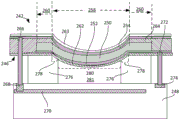
In fig. 2A, a convex or dome-shaped vibration element 202 is shown. The convex vibratory element 202 includes a top surface 204 that is exposed and forms a portion of the vibrating outer surface of the transducer array (e.g., along with the top surfaces of the other vibratory elements in the transducer array). The vibrating element 202 also includes a bottom surface 206 attached to a top surface of a base 208.
As shown in fig. 2A, the dome-shaped vibrating element 202 includes a convex or dome-shaped piezoelectric element 210 disposed between a reference electrode 212 and a drive electrode 214. In this example, the reference electrode 212 is disposed above the top surface (distal from the substrate 208) of the convex piezoelectric element 210, while the drive electrode 214 is disposed below the bottom surface (proximal to the substrate 208) of the convex piezoelectric element 210. In an alternative example (not shown), the drive electrode may be disposed above the top surface of the convex piezoelectric element while the reference electrode is disposed below the bottom surface of the convex piezoelectric element.
As shown in fig. 2A, the convex piezoelectric element 210 is a thin layer of piezoelectric material having substantially the same thickness throughout. The thin layer of piezoelectric material includes a bend 218 surrounded by a planar portion 220. The central flexure 218 is bent away from the base 208 to which the vibrating element 202 is attached. For example, the convex piezoelectric element 210 can be formed by depositing (e.g., sputtering) particles of piezoelectric material in a uniform layer on a profile-transferring base layer having a dome formed on a planar top surface. An example piezoelectric material that may be used to form the piezoelectric element 210 includes lead zirconate titanate (PZT).
As further shown in fig. 2A, the convex piezoelectric element 210 is disposed above the drive electrode 214, on the top surface of the drive electrode 214. The drive electrode 214 may be a thin layer of conductive material having a top surface that contacts and conforms to the bottom surface of the convex piezoelectric element 210. Thus, the drive electrode 214 also includes a central curved portion that curves away from the substrate 208 and a planar portion that adjoins (e.g., surrounds) the central curved portion. The central curved portion of the drive electrode 214 and the central curved portion of the convex piezoelectric element 210 have matching surface profiles.
In some embodiments, the drive electrode 214 may be formed by depositing a thin layer of conductive material on a profile-transferring base layer having a dome formed on a planar top surface. After the layer of conductive material (i.e., the drive electrode layer in this example) is deposited on the profile-transferring base layer, then the deposited drive electrode layer may serve as the profile-transferring base layer upon which the thin layer of piezoelectric material of the piezoelectric element 210 may be deposited. For example, the conductive material for the drive electrode layer may include various metals (e.g., Au, Pt, Ni, I)r, etc.), alloys (e.g., Au/Sn, Ir/TiW, Au/TiW, AuNi, etc.), metal oxides (e.g., IrO2、NiO2、PtO2Etc.) or combinations thereof.
In some embodiments, suitable methods for depositing the piezoelectric material on the drive electrode layer include, for example, sputtering, chemical vapor deposition, physical vapor deposition, atomic layer deposition, plasma enhanced chemical vapor deposition, and the like. Types of sputter deposition may include magnetron sputter deposition (e.g., RF sputtering), ion beam sputtering, reactive sputtering, ion beam assisted deposition, high utilization target sputtering, and high power pulsed magnetron sputtering. The thickness of the piezoelectric layer can be selected such that the piezoelectric element 210 is flexible enough to bend under a driving voltage, yet strong enough to transmit its vibration to a propagation medium in contact with the exposed outer surface 204 of the vibrating element 202.
As further shown in fig. 2A, a reference electrode 212 is disposed above the top surface of the convex piezoelectric element 210. The reference electrode 212 may be a thin layer of conductive material with a bottom surface in contact with and conforming to the top surface of the convex piezoelectric element 210. Thus, the reference electrode 212 also includes a central curved portion that curves away from the substrate 208 and a planar portion that adjoins (e.g., surrounds) the central curved portion. The central curved portion of the reference electrode 212 and the central curved portion of the convex piezoelectric element 210 have matching surface profiles.
In some embodiments, for example, after the deposited piezoelectric layer has been patterned to define the piezoelectric element 210, the reference electrode 212 may be formed by depositing a thin layer of conductive material on the deposited piezoelectric layer. For example, the conductive material for the reference electrode layer can include various metals (e.g., Au, Pt, Ni, Ir, etc.), alloys (e.g., Au/Sn, Ir/TiW, Au/TiW, AuNi, etc.), metal oxides (e.g., IrO2、NiO2、PtO2Etc.) or combinations thereof.
As further shown in FIG. 2A, in some embodiments, the vibrating element 202 optionally includes a thin film layer 222 underlying the drive electrode 214 and in contact with a bottom surface of the drive electrode 214. In some embodiments, to form the vibrating element 202, the thin film layer 222 may first be deposited on a dome-shaped profile-transferring substrate. The drive electrode layer may then be deposited on the top surface of the thin film layer 222. After the drive electrode layer is deposited, a piezoelectric layer can be deposited on the drive electrode layer. The piezoelectric layer and the drive electrode layer may be patterned to form separate drive electrodes 214 and piezoelectric elements 210 before the reference electrode layer is deposited on the piezoelectric elements. In some embodiments, the profile-transferring base layer on which the film layer 222 is deposited may be etched away from bottom to top to expose a central curvature of the bottom surface of the film 222, such that the central curvature may be curved under an applied voltage. In some embodiments, the film layer 222 may be an oxide layer that serves as an etch stop for the etching process.
In some embodiments, dielectric film 224 layer (e.g., SiO) is formed after piezoelectric element 210 is formed on the top surface of drive electrode 214 and before the deposition of the reference electrode layer2、SiN2Or a combination thereof) may be deposited on the top surface of the piezoelectric element 210. The central portion of the membrane 224 above the central portion of the curved portion 218 of the piezoelectric element 210 may be etched open to expose the central top surface of the piezoelectric element 210. A reference electrode layer may then be deposited on the exposed top surface of the piezoelectric element 210 such that the bottom surface of the reference electrode 212 contacts and conforms to the exposed top surface of the dielectric film 224 and the exposed top surface of the piezoelectric element 210. A dielectric film 224 may be used to insulate the drive electrode 214 from the reference electrode 212. In addition, the dielectric film 224 may also serve to insulate the reference electrode 212 from the piezoelectric element 210 (e.g., including the perimeter portion 238 and the planar portion 220 of the piezoelectric element 210) in regions of the piezoelectric element 210 that remain stationary during operation. By insulating the reference electrode 212 from the piezoelectric element 210 in the regions that remain stationary, the internal stress experienced by the piezoelectric element due to the drive voltage applied in those regions can be reduced.
In some embodiments, where only a small number of vibrating elements are present in the transducer array, electrical connections to the drive and reference electrodes of each vibrating element may be made via conductive traces extending in the same plane parallel to the top surface of the substrate 208. In some embodiments, the reference electrodes of several vibrating elements may be connected to form a common reference electrode across multiple vibrating elements. In some embodiments, where many vibrating elements are distributed in a small lateral area, there may not be enough space between the individual vibrating elements to have the conductive traces extend in a single plane parallel to the top surface of the substrate 208. Alternatively, respective vertically oriented electrical interconnects may be made for each of some or all of the vibrating elements in the transducer array to connect the vibrating elements to the control/sensing circuitry in the substrate 208. As shown in FIG. 2A, vertically oriented electrical interconnects 226 are used to electrically connect the drive electrodes 214 to active connection pads 228 of control/sense circuitry 230 in the substrate 208. In addition, vertically oriented electrical interconnects 232 are used to electrically connect the reference electrode 212 to a ground pad 234 of the control/sensing circuitry 230 in the substrate 208. In some embodiments, where a common reference electrode is used across the entire transducer array, only one electrical connection is required to electrically connect the common reference electrode to a ground pad in the substrate 208.
In some embodiments, as shown in fig. 2A, the flexible portion of the vibrating element 202 may be suspended above the top surface of the substrate 208. The space between the top surface of the base 208 and the bottom surface 206 of the vibrating element 202 may be a support 236, such as an annular support, having a hole 241 vertically aligned with the flexure 218 of the vibrating element 202. The support 236 has a bottom surface attached to the top surface of the base 208 and a top surface attached to the bottom surface 206 of the vibration element 202. In embodiments where the membrane 222 is not present under the drive electrode 214, the bottom surface of the drive electrode may serve as the bottom surface 206 of the vibrating element 202. If a membrane 222 is present, the bottom surface of the membrane 222 may serve as the bottom surface of the vibration element 202. The supports 236 may also be used to insulate individual vibrating elements located on the substrate 208 to reduce cross-talk between adjacent vibrating elements. In some embodiments, the height of the support may be sufficiently small such that only a small gap (e.g., a few microns) exists between the central vibrating portion (in other words, the flexible portion) of the vibrating element 202 and the top surface of the substrate 208. In some embodiments, the height of the support 236 may be thicker, such as 10-50 microns or thicker.
In the example configuration shown in fig. 2A, the reference electrode 212 is positioned above the piezoelectric element 210, while the drive electrode 214 is positioned below the piezoelectric element 210. In an alternative configuration, the reference electrode may be positioned below the piezoelectric element, while the reference electrode is positioned above the piezoelectric element. A vibrating element having an alternative configuration may be formed in a similar manner to that described above, except that the lower metal layer may be used as the reference electrode layer and the upper metal layer may be used as the drive electrode layer. Furthermore, the vertically oriented electrical interconnects all reach into different metal layers in the vibrating element.
With continued reference to the example shown in fig. 2A, in some embodiments, a protective film (not shown) (e.g., a non-wetting coating, a PECVD oxide coating, etc.) may be deposited on the top surface of the reference electrode 212. In some embodiments, the protective film may be a continuous layer deposited over the entire top surface of the transducer array. The top surface of the protective film may be exposed and no additional layers deposited on top. In operation, the exposed top surface of the optional protective film may be in direct contact with a propagation medium (which may be a material of interest, such as tissue, or a coupling medium, such as an ultrasound transmissive gel) so that vibrations of the vibrating elements in the transducer array may be coupled to pressure waves in the propagation medium.
The optional protective film may protect the vibrating element 202 from dust and contamination, as well as possible corrosion due to moisture or other substances in the propagation medium. Furthermore, in embodiments where the drive electrode is placed above the piezoelectric element 210 and the reference electrode is placed below the piezoelectric element 210, a protective membrane may be advantageous in embodiments where the protective membrane may act as an insulating layer between the drive electrode (now positioned on top of the vibrating element) and the propagation medium (e.g. the skin or tissue of the patient).
In some embodiments, no protective film is used in the vibrating element 202, and the top surface of the reference electrode 212 may be directly exposed to the propagation medium when in use. For example, where a continuous reference electrode is used to cover the entire transducer array and the continuous reference electrode is made of an inert metal that is resistant to corrosion and contamination (e.g., Au or Pt), then the continuous reference electrode may serve as the exposed outer surface of the transducer arrangement for coupling the vibration of the vibrating element to the propagation medium, with the reference electrode held at ground potential.
In some embodiments, as shown in fig. 2A, the flexures of the vibrating element 202 (including the central flexures of the reference, piezoelectric, and drive electrodes, and any additional membrane layers above, below, or between the reference, piezoelectric, and/or drive electrodes) remain curved in the absence of any applied voltage between the drive and reference electrodes. When a time-varying driving voltage is applied between the driving electrode 214 and the reference electrode 212, the bent portion (or the central bent portion thereof) of the vibration element 202 may vibrate in response to the time-varying driving voltage.
In some embodiments, only the planar portion of the vibrating element 202 is fixed to the base 208 (e.g., by the support 236) and remains stationary during operation, while the entire curved portion of the vibrating element 202 vibrates in response to a time-varying drive voltage. However, in some embodiments, the perimeter portion 238 of the flexure may also be secured to the substrate 203 by supports 236 such that the perimeter portion 238 of the flexure may remain stationary during operation while only the central portion 240 of the flexure vibrates in response to a time-varying drive voltage. In some embodiments where the perimeter portion 238 of the flexure is secured to the substrate, all or some of the planar portions of the vibrating element may be eliminated.
In some embodiments, the perimeter portion 238, which is fixed and remains stationary, may occupy only a small width relative to the transverse dimension of the flexure 218. As will be shown later in the specification, by keeping the small peripheral portion 238 of the flexure 218 stationary during operation, stress at the transition point between the flexure 218 and the flat portion 220 of the piezoelectric element 210 can be reduced, thereby extending the life of the vibrating element 210.
In some embodiments, where the perimeter portion 238 of the flexure 218 of the piezoelectric element 210 is fixed and remains stationary during operation, the size of the planar portion 220 surrounding the perimeter portion 238 of the flexure 218 may be reduced or eliminated entirely from the vibrating element 202, so long as the holding force provided by the support 236 to the perimeter portion 238 is sufficiently strong and durable to prevent delamination of the piezoelectric element 210 from the electrodes 212 and 214 during an acceptable life of the piezoelectric transducer device.
Fig. 2B shows another example configuration of the vibration element 242, in which a concave piezoelectric element 250 is used. The vibrating element 242 may be configured similarly to the vibrating element 202, except as described below. In the example vibration element 242, the reference electrode 252 is disposed below the bottom surface of the concave piezoelectric element 250, and the drive electrode 254 is disposed above the top surface of the concave piezoelectric element 250. An optional membrane layer 262 may be disposed below the bottom surface of the reference electrode 252. The bottom surface 246 of the vibrating element 242 may be the bottom surface of the membrane layer 262 (if present) or the bottom surface of the reference electrode 252 (if the membrane layer 262 is not used). In addition, a dielectric layer 264 may be deposited on the piezoelectric element and the reference electrode layer to insulate the drive electrode 254 from the reference electrode 252 and to insulate the drive electrode 154 from the piezoelectric element 250 in regions other than the central region on the top surface of the piezoelectric element 250.
In addition, an optional protective film 263 may be used to cover the top surface of the driving electrode 254. The top surface of the protective film 263 may serve as an exposed top surface of the vibration element 242 and be in contact with a propagation medium during operation. In some embodiments, the protective film 263 is a thin dielectric layer that serves to insulate the drive electrode 254 from the propagation medium.
Further, vertically oriented electrical interconnects 266 may electrically connect the drive electrodes 254 to active connection pads 268 of control/sense circuitry 270 in the substrate 248. Vertically oriented electrical interconnects 272 may electrically connect the reference electrode 252 to a ground pad 274 of the control/sensing circuitry 270 in the substrate 248. In some embodiments, the reference electrode 252 may be a continuous conductive layer that spans the entire transducer array in the transducer device.
Although the example shown in FIG. 2B has the reference electrode 252 disposed closer to the substrate 248 and the drive electrode 254 disposed further from the substrate 248, in alternative embodiments, the positions of the reference electrode 252 and the drive electrode 248 may be reversed. When the positions of the reference electrode 252 and the drive electrode 254 are reversed, the lengths of the electrical interconnects 266 and 272 may be adjusted to connect to the appropriate electrodes in the vibrating element 242.
As shown in FIG. 2B, the vibrating element 242 is similar to the vibrating element 202 shown in FIG. 2A, except that the piezoelectric element 250, the drive electrode 254, and the reference electrode 252 each include respective flexures that flex toward the substrate 248. In some embodiments, the concave reference electrode 252, the piezoelectric element 250, and the drive electrode 254 may be formed by sequentially depositing a reference electrode layer, a piezoelectric layer, and a drive electrode layer on a top surface of a profile-transferring base layer having a concave portion (or an inverted dome) surrounded by a planar portion.
In some embodiments, similar to the vibrating element 202 as shown in fig. 2A, the peripheral portion 278 of the flexure portion 258 of the vibrating element 242, except for the planar portion 260 of the piezoelectric element 242, also remains stationary during operation, while only the central portion 280 of the flexure portion 258 vibrates in response to a time-varying drive voltage.
Although fig. 2A and 2B illustrate electrical interconnects 226, 232, 266, 272 contacting the bottom surfaces of electrodes 214, 212, 254, 252 in some embodiments, the electrical interconnects may contact the top surfaces of the electrodes.
In some embodiments, the vibrating element 242 is suspended above the base 248 and attached to the base 248 by a support 276 (e.g., an annular support having an aperture 281 aligned with the flexure 258 of the piezoelectric element 250). Since the concave-shaped vibration element 242 is used in the example configuration shown in fig. 2B, the space between the bottom surface 246 of the vibration element 242 and the top surface of the substrate 248 should be large enough to keep the bottom of the vibrating portion 280 out of contact with the top surface of the substrate 242 when the vibration element 242 generates the maximum displacement under a driving voltage or an impact pressure. Therefore, the thickness of the support 276 should be selected to accommodate the expected maximum displacement of the vibrating element 242.
Although the support 276 is used to support and suspend the vibratory element shown in fig. 2A and 2B, in some embodiments, a cavity may be formed in the substrate (e.g., substrate 208 or 248) below the flexible portion of the vibratory element (e.g., vibratory element 202 or 242) to create space for accommodating displacement of the vibratory element during operation (e.g., driving and/or sensing). Alternatively, the electrical interconnects 226, 272 may be supports (e.g., ring supports) that define the height between the vibrating elements 202, 252 and the bases 208, 248 in place of the supports 236, 276.
Although fig. 2A and 2B illustrate the piezoelectric elements 210, 250 as discrete elements of a single vibrating element, the piezoelectric elements may be a continuous layer for multiple vibrating elements.
Although fig. 2A and 2B show the vibrating elements 202, 242 curved, the vibrating elements may alternatively be flat. Fig. 3A is a schematic diagram illustrating deformation of a convexly curved piezoelectric element 302 under an applied voltage (e.g., during driving) and an applied mechanical pressure (e.g., during sensing).
In fig. 3A, it is assumed that the piezoelectric element 302 has a as-deposited polarization direction which is directed from the left surface of the piezoelectric element 302 to the right surface of the piezoelectric element 302 and is locally perpendicular to both surfaces of the piezoelectric element 302. It is further assumed that a drive electrode (not shown) is disposed adjacent to the left surface of the piezoelectric element 302 and a reference electrode (not shown) is disposed adjacent to the right surface of the piezoelectric element 302. For example, this configuration corresponds to the configuration shown in fig. 2A. Based on the above configuration, a positive voltage applied to the piezoelectric element 302 between the drive electrode and the reference electrode may cause an electric field in the piezoelectric element 302 that is directed from the left surface to the right surface of the piezoelectric element 302. In other words, the applied positive voltage results in an electric field in the piezoelectric element 302 that is locally aligned and parallel to the polarization direction in the piezoelectric element 302. As a result, the piezoelectric element 302 contracts, the bending portion of the piezoelectric element 302 retracts to the left (shown as piezoelectric element 302 "), and the center O of the bent vibration element 302 moves along its central axis from the rest position 304 to a new position 308 to the left of the position 304. When the applied positive voltage is removed, the flexure of the piezoelectric element 302 expands back to its original shape, and the center O of the flexed vibrating element 302 returns to its original resting position 304. The vibration of the piezoelectric element 302 may transmit pressure waves 310 into the propagation medium 303 located to the right of the piezoelectric element 302.
In some embodiments, when a negative voltage is applied across the piezoelectric element 302 between the drive electrode and the reference electrode, the piezoelectric element 302 can expand and the center O of the curved piezoelectric element 302 (now shown as 302') can move further to the right of the rest position 304 to a new position 306. When the negative voltage is removed, the center O of the curved piezoelectric element 302 may return to its original rest position 304.
In some embodiments, a drive signal comprising alternating negative and positive voltage signals may be used to vibrate the vibratory element between a maximum positive displacement position and a maximum negative displacement position (e.g., positions associated with center positions 306, 308). In some embodiments, only positive voltages are used to drive the vibrating element, and a positive voltage signal may be applied as a pulse above a constant reference voltage. In some embodiments, it is advantageous to avoid using a negative voltage signal when driving the vibrating element. For example, in the configuration shown in fig. 3A, a negative drive voltage may induce an electric field anti-parallel to the polarization direction of the piezoelectric element 302, which tends to depolarize the piezoelectric element 302 and cause the performance of the piezoelectric element 302 to deteriorate over time.
In some implementations, when the vibrating element is in the sensing mode and no voltage is applied to the curved piezoelectric element 302, the curved piezoelectric element 302 can deform in response to the applied mechanical pressure. For example, when a pressure wave in the propagation medium 303 reflects back to the vibrating element and is intercepted by the exposed surface of the vibrating element, the curved surface of the piezoelectric element 302 may be pushed from the rest position to a position to the left of the rest position. The center O of the curved piezoelectric element 302 may move from the rest position 304 to a new position to the left of the rest position 304. Due to the deformation, a voltage difference is generated between the left and right surfaces of the vibration element 302. The timing and strength of the voltage difference can be used to determine the change in density and elastic modulus in the propagation medium 303 (and thus the location of the object or structure change in the propagation medium 303) that would result in the reflection of the pressure wave in the propagation medium 303.
In some embodiments, the same vibrating elements in the transducer array may be used to both drive pressure waves in the propagation medium 303 and to sense pressure waves reflected from the propagation medium 303. The vibrating element may be switched between drive and sense modes based on control signals generated by switching circuitry in the substrate. In some embodiments, the vibrating elements used for driving and sensing may be separated in the transducer array, e.g., the driving vibrating elements and the sensing vibrating elements may be alternately distributed in the transducer array and operated synchronously.
Although fig. 3A shows a dome-shaped or convex piezoelectric element 302 having a dephasing direction pointing to the right, the same principles for driving and sensing vibration of a dome-shaped piezoelectric element are also applicable to driving and sensing vibration of a concave or convex piezoelectric element.
For example, as shown in fig. 3B, assuming that the concave piezoelectric element 322 has a dephasing direction pointing from the left surface to the right surface of the piezoelectric element 322, a drive electrode (not shown) is disposed on the left side of the concave piezoelectric element 322, and a reference electrode (not shown) is disposed on the right side of the concave piezoelectric element 322.
According to the above configuration, when a positive voltage is applied between the drive electrode and the reference electrode, an electric field can be induced in the piezoelectric element 322. The induced electric field is aligned and parallel to the polarization direction of the piezoelectric element 322. As a result, the piezoelectric element 322 may contract (e.g., as represented by piezoelectric element 322'), and the center O of the flexed piezoelectric element 322 may be displaced to a new position 326 to the right of the resting position 324. When the positive voltage is removed, the piezoelectric element 322 returns to its original resting shape. The vibration of the vibrating element 322 excites a pressure wave 330 in the propagation medium 333 which is in contact with the exposed concave surface of the vibrating element.
Similarly, when the reflected pressure wave exerts mechanical pressure on the concave right surface of the vibrating element 322, the piezoelectric element 322 may extend to the left (e.g., as represented by piezoelectric element 322 "). The center O of the piezoelectric element 322 can be moved from its rest position 324 to a new position 328, and a voltage difference can be generated between the left and right surfaces of the piezoelectric element 322. The timing and strength of the voltage difference can be used to determine the change in density and elastic modulus in the propagation medium 333 and infer the location of an object or structure change in the propagation medium 333 that would cause a reflected pressure wave.
As previously described, sputtered piezoelectric material can have a large as-deposited polarization. Some environments for sputtering piezoelectric materials include Direct Current (DC) biasing during sputtering. The DC field causes the piezoelectric material to polarize in the direction of the DC field. In some embodiments, the as-deposited polarization direction in the deposited piezoelectric layer (e.g., sputtered PZT) can be locally perpendicular to the underlying profile-transferring base layer surface and directed away from the base layer surface.
If the desired polarization direction in the piezoelectric element is different from the as-deposited polarization direction, the piezoelectric film is deposited on the profile-transferring base layer, then flipped over, and bonded to another base layer to obtain the desired polarization direction.
Although fig. 3A and 3B show curved piezoelectric elements 302, 322, the piezoelectric elements may alternatively be flat.
Fig. 4A shows a Scanning Electron Microscope (SEM) image 400 of a partial cross-section of a convex piezoelectric film. Image 400 shows the grain structure of a sputtered PZT layer 402 deposited on a dome-shaped iridium electrode layer 404. A dome-shaped iridium electrode layer 404 is suspended over the silicon-based layer.
The particle structure within the PZT layer 402 is substantially cylindrical, with all or almost all of the cylindrical particles being locally perpendicular to the surface of the curved PZT layer 402. The aligned columnar PZT particle structure shown in fig. 4A occurs when PZT is gradually deposited or grown on a curved underlayer (e.g., on a curved surface of an etch stop layer or a profile-transferring base layer). Aligned columnar grain structures locally perpendicular to the curved surface of the piezoelectric film do not inherently appear in the bulk of the piezoelectric material ground into a curved film. Such grain alignment and orientation also does not inherently occur in injection molded curved piezoelectric films.
When the grain structure in the sputtered PZT film is aligned and locally perpendicular to the curved surface of the PZT film, the amount of local internal stress present in the film during vibration of the film is reduced compared to films having randomly oriented grain structures (e.g., films formed from bulk PZT or injection molding). With a reduced amount of local internal stress, PZT films with columnar particles aligned as shown in fig. 4A can have a longer useful life than films produced using other conventional methods (e.g., by grinding or by injection molding).
Fig. 4B is an enlarged SEM image 410 of the curved sputtered PZT film 402 near the transition region 412 between the curved portion and the planar portion of the sputtered PZT film 402. The grain structure of the sputtered PZT in the transition region 412 is squeezed toward the center of the transition region 412. The transition region 412 is less robust during vibration than other more uniform regions in the sputtered PZT film 402 where the particle structures are better aligned and parallel.
Generally, during operation, a relatively large amount of stress is generated in the piezoelectric film near the boundary between the vibrating portion and the stationary portion of the piezoelectric film. As a result, if the transition point between the flat portion and the curved portion of the piezoelectric film 402 is accurately placed at the transition point between the vibrating portion and the stationary portion of the piezoelectric film 402 (e.g., when the piezoelectric film 402 is fixed to the substrate only at the flat portion and not at the curved portion of the piezoelectric film 402), the piezoelectric film 402 tends to break after excessive use.
In some embodiments, the perimeter of the curved portion of the PZT film 402 can be secured to a substrate and remain stationary during operation (e.g., as shown in the configurations in fig. 2A-2B). In other words, the weaker transition point between the curved portion and the flat portion in the piezoelectric film 402 moves away from the transition point between the vibrating portion and the stationary portion of the piezoelectric film 402. Alternatively, the transition point between the vibrating portion and the stationary portion moves to a more powerful, better aligned uniform portion of the piezoelectric membrane 402 (e.g., a bend of the piezoelectric membrane 402). By moving the high stress areas to stronger areas in piezoelectric film 402, piezoelectric film 402 is less prone to fracture due to internal stresses generated during vibration of piezoelectric film 402.
Although fig. 4A and 4B illustrate a curved piezoelectric film including a sputtered piezoelectric layer 402 and electrode layer 404, the piezoelectric film may alternatively be flat. A flat sputtered piezoelectric layer has the same benefits of a columnar grain structure as a curved sputtered piezoelectric layer. The columnar grain structure is locally perpendicular to the surface of the planar piezoelectric layer. Because the planar piezoelectric layer is planar, it does not have a transition region between the curved portion and the planar portion. Thus, the flat piezoelectric film has better flexibility in the case where it is attached to the substrate.
2A-4B illustrate example designs and structures of individual vibratory elements that may be used in a transducer array of a transducer device. The piezoelectric transducer device may include one or more transducer arrays, each transducer array including a plurality of vibrating elements. Fig. 5A illustrates an example hexagonal transducer array 502 that may be included in an ultrasonic transducer device 504. In an example embodiment, about 1000 vibrating elements 506 having a size of 25 microns may be distributed within hexagonal array 502 having a lateral dimension of about 3 mm. In another example embodiment, about 400 vibrating elements having a size of 60 microns may be distributed in a hexagonal array having a lateral dimension of about 3 mm. In yet another embodiment, about 378 vibratory elements having a size of 60 microns can be distributed in a square array having a lateral dimension of 2.13 mm. The above dimensions are illustrative and other dimensions and array sizes, spacings and layouts of the vibrating elements are possible. For example, the above example dimensions are applicable to ultrasound devices used in intravascular diagnostic or therapeutic applications.
Figure 5B illustrates a perspective view of a cross-section of the transducer array 502 in the transducer device 504 shown in figure 5A. As shown in fig. 5B, the top surface 508 of the transducer array 504 is exposed and may be in contact with a propagation medium. When the top surfaces of the vibrating elements 506 in the transducer array 502 vibrate in response to a driving voltage, the vibration of the top surfaces of the vibrating elements 506 may cause pressure waves to be generated in the propagation medium.
As shown in fig. 5B, the vibrating element 506 in the transducer array 502 includes a vibrating portion 510, the vibrating portion 510 suspended over a cavity or aperture 512 created by a ring-shaped support (e.g., a ring-shaped metal seal 514) attached to the vibrating portion 510 and to a top surface of a substrate 516. An annular metal seal 514 is attached to the planar portion of the vibrating element 506 and the peripheral portion of the curved portion of the vibrating element 506. In addition, the annular metal seal 514 supporting each vibratory element 506 is insulated from the annular metal seals supporting the other vibratory elements 506, e.g., by an air or vacuum gap 518. In some embodiments, the thickness and width of the annular seal 514 are selected such that the seal 514 substantially prevents vibrational crosstalk between adjacent vibratory elements 506 in the transducer array 502. In some embodiments, a support layer may be placed within the cavity 512 over the top surface of the substrate 516 to absorb energy transferred to the vibrating element 506 from reflected pressure waves in order to reduce noise in the sensing signal and echoes within the cavity 512 caused by vibrations of the vibrating element 506.
Although fig. 5B shows a curved vibrating element 506, the vibrating element may alternatively be flat.
In some embodiments, the annular metal seal 514 may be formed by a eutectic bonding process. For example, the vibrating elements 506 and the substrate 516 of the transducer array 502 may be prepared in separate processes. Metals that can be bonded using eutectic bonding techniques can then be plated at corresponding locations on the bottom surface of the array of vibrating elements 506 and the top surface of the substrate 516, respectively. The array of vibratory elements 506 may then be bonded to a substrate 516 at the locations plated with metal. The bonded metal may form an annular seal 514 that attaches the vibrating element 506 to a substrate 516. In some embodiments, other suitable materials (e.g., ceramics) may be used to form the seal.
In some embodiments, substrate 516 includes an ASIC layer for providing control signals to the vibrating element and for processing (e.g., compressing, packaging, and transmitting) sensing signals received from the vibrating element. Thus, in addition to the annular seal 514, electrical connection pads and connection bumps may be plated on the top surface of the substrate 516 (leading to the electrical ground and active elements of the drive/sense circuitry in the ASIC layer of the substrate 516). Corresponding electrical connection pads and connection bumps may be plated on the bottom surface of the transducer array 502, where the connection pads are electrically connected to the individual drive electrodes of the vibrating elements 506 in the transducer array 502.
The ASIC layer in the substrate 516 includes an array of driving or sensing integrated circuits corresponding to the transducer array 502, e.g., one circuit for each vibrating element 506. Each circuit in the array of ASIC layers may have the same circuit structure and function. There is also an array of vertically extending electrical interconnects corresponding to the transducer array 502 and to the array of circuits in the ASIC layer, for example at least one vertically extending electrical interconnect for each vibrating element 506 to connect to the drive electrodes of the vibrating element 506. If there is a common reference electrode for the transducer array 502, at least one vertically extending electrical connection connects the ASIC layer in the substrate 516 to the reference electrode. There may be an array of vertically extending electrical connections for the reference electrode, although there may be fewer vertically extending electrical connections for the drive electrode. If there is a reference electrode for each vibrating element, there are vertically extending electrical connections for each reference electrode, i.e. two vertically extending electrical connections for each vibrating element, one for the drive electrode and one for the reference electrode.
Vertically extending electrical interconnects may be provided by the annular seal 514 or other conductive elements, such as vertically oriented electrical interconnects 232 (see fig. 2A) connected to the pads 520. Thus, each vibratory element 506 may be connected to associated circuitry in the ASIC by an associated vertically extending interconnect. In this configuration, the leads from the vibrating element do not require significant space on the face of the transducer array. Thus, the vibrating element 506 may be more tightly packed, which may improve image quality, as compared to systems having laterally extending leads.
When the bottom surface of the transducer array 502 and the top surface of the substrate 516 are bonded together at the metal ring seal 514 (e.g., by a eutectic bonding process), the electrical connection bumps plated on the bottom surface of the transducer array 502 may be bonded (e.g., by a eutectic bonding process) to the electrical connection bumps plated on the top surface of the substrate 516 to form vertically oriented electrical interconnects that electrically connect the individual drive electrodes in the transducer array 502 to their respective drive and/or sense circuits located in the ASIC layer of the substrate 516. Further, in some embodiments, the ground electrode may be a shared common ground electrode, and a single vertically oriented interconnect may be implemented between the ground electrode and an electrical ground in the ASIC layer of the substrate 516. For example, a single vertically oriented interconnect for the reference electrode may also be formed using a eutectic bonding process.
Fig. 5C shows an enlarged top view of the transducer array 502 showing the flexible portion of the vibrating element 506, the annular seal 514 supporting the flexible portion, and the electrical connection pads 520 to the drive electrodes. In some embodiments, the drive electrodes are located at the bottom of the vibrating element 506, and electrical connections to the drive electrodes may run directly vertically down from electrical connection pads in the drive electrode layer to corresponding connection pads in the top surface of the substrate 516. In some embodiments, the drive electrode is located on top of the vibrating element 506, and electrical connections to the drive electrode can travel vertically downward from the electrical connection pads in the drive electrode layer, through corresponding openings in the piezoelectric layer and the reference electrode layer, to the electrical connection pads located on the top surface of the substrate 516.
As previously described herein, the size (e.g., radius) of the vibrating portion of the vibrating element 506 and the spacing (or pitch) of the vibrating elements 506 in the transducer array 502 may be selected based on the desired imaging resolution of the ultrasound transducer device 504. The smaller the size of the vibrating elements and the space/spacing between the vibrating elements, the better the resolution of the ultrasonic transducer. In some embodiments, the flexible portion of the vibration element 506 may have a size (e.g., radius) in the range of 20 microns to 70 microns. The size of the transducer device array may be selected based on the desired imaging area and the desired size of the transducer device 504. For example, for intravascular applications, the array size can be made less than 2mm in at least two orthogonal directions.
In some implementations, the height of the curved vibrating elements in the transducer array (e.g., the height of the dome-shaped or concave-shaped piezoelectric elements) may be selected based on the desired operating range or resonant frequency and the appropriate impedance for matching the impedance of the intended propagation medium. For example, for an ultrasonic transducer, the resonant frequency may be in the range of 20KHz to 30 MHz. For medical use, the resonance frequency is typically in the range of 1MHz to 15 MHz. For example, the thickness of the piezoelectric element in the vibration element 506 may be in the range of 3 to 6 micrometers. For example, the height of the curved piezoelectric element may be from 1.5 microns to 10 microns. The resonant frequency and impedance of the transducer array are highly tuned to suit the needs in various applications. In an exemplary embodiment, for a dome-shaped vibrating element having a radius of 50 microns and a vertex angle of 25 degrees, the resonant frequency is about 14.3MHz and the electrical impedance is about 1.2 kilo-ohms at 15 MHz. The amount of displacement is about 82 angstroms per volt.
In some embodiments, the drive voltage for the micro-dome/concave transducer array may be 5-10 volts to obtain a signal strength comparable to that obtainable using conventional ultrasonic transducer devices driven at 100-200 volts or higher. For example, ultrasound transducer devices based on micro-dome/concave arrays may have a drive efficiency of up to 3MPa/V at 15MHz drive frequency. As a receiver, the ultrasound transducer device based on the micro-dome array may have a sensitivity up to 0.5 μ V/Pa at a drive frequency of 15 MHz. Furthermore, micro-dome/concave based transducer arrays may have insertion losses as high as 50% (6dB) compared to the 20dB losses in other conventional transducer technologies.
In some embodiments, each vibrating element in a micro-dome/concave transducer array may be made quite small compared to the ultrasonic wavelengths that the transducer array may produce, based on the semiconductor manufacturing processes described herein. In addition, the spacing between adjacent vibrating elements is not limited to the size of the cutting blade used to make the vibrating elements from a bulk piezoelectric material. Because the transducer array may be made of small vibrating elements and have a pitch less than half the drive wavelength, each vibrating element may act as a point source for emitting waves with a uniform circular wavefront. Thus, the entire vibrating transducer array may be used to form a beam having a desired wavefront direction, focus, and shape without any undesirable side lobes. Furthermore, the omnidirectional radiation pattern of the vibrating elements also creates a larger acceptance angle of the transducer arrangement due to the radiation pattern of the vibrating elements located at the edge of the transducer array.
Although, as previously mentioned, there may be conductive traces to individual vibrating elements in the transducer array in the same plane as the drive electrodes of the vibrating elements, such traces are only possible when a small number of vibrating elements are present in the transducer array (e.g., a 4 x 4 array) and the space between the vibrating elements is large enough (e.g., 20-30 microns). When a high resolution compact transducer arrangement is desired, an integrated ASIC layer positioned directly below the transducer array may be implemented, wherein vertically oriented electrical interconnects may be formed between the drive electrodes in the transducer array and the integrated ASIC layer. A high resolution compact transducer device may have, for example, more than 200 vibrating elements, for example 1000 or more vibrating elements; a pitch of less than about 200 microns, such as between 100 and 200 microns, 65 microns or less or 30 microns or less; and/or a resolution of less than about 0.25mm, such as 0.1mm or less or 0.06mm or less.
For example, when a large number (e.g., 1000) of vibrating elements are tightly packed within a small area (e.g., within a 3mm radius circle), there is not enough space in the same plane as the drive electrodes for individual traces to extend from the drive electrodes. Alternatively, vertically oriented electrical connections may be made from small electrical connection pads for each drive electrode to an integrated ASIC layer in the substrate located below the transducer array. The integrated ASIC layer may have a plurality of circuit layers made of NMOS transistors. The design of the ASIC layer may accommodate a large number of individually controlled outputs (e.g., 1000-. The same external input connection may also serve as an output connection to send the sensed voltage signal to an external imaging device.
Fig. 6 illustrates example functions that may be implemented in an integrated ASIC layer in a substrate of a transducer device 602 that includes a micro-dome/concave transducer array. The integrated ASIC layer can significantly reduce the number of external connections required to use the transducer device. Fewer external connections results in a reduction in the overall size of the transducer arrangement. Furthermore, more data processing may be performed on the board within the ASIC layer of the transducer arrangement, and thus, external equipment for processing the signals required to drive the transducer array and analyzing the signals received from the transducer array may also be reduced or simplified.
As shown in fig. 6, in some embodiments, the composite control signal may be provided to the ASIC layer via a small number of external input connections of the ASIC layer. The composite control signal may be deserialized by a deserializer 604. The deserialized control signal may be demultiplexed by the demultiplexer 606 and the corresponding timing control for the demultiplexed signal may be added to the demultiplexed signal. The digital-to-analog converter 608 may be implemented in the ASIC layer to convert analog control signals to drive voltage signals for individual vibrating elements in the transducer array. A corresponding time delay may be added to the individual drive voltage signals by the programmable time delay controller 610 to produce the desired beam shape, focus and direction. The switch 612 may be implemented to switch the operation of the transducer array between a drive mode and a receive mode. When the transducer arrangement 602 is in a receive mode, the received voltage signal may be converted to an analog signal using the analog-to-digital converter 614. The analog signal is compressed by a data compression unit 616 and multiplexed by a multiplexer 618. The multiplexed signal may be serialized by the serializer 620 and sent back to the external processing device via an external output connection of the ASIC layer (e.g., the same external connection used to receive the input during the drive mode). The above-described functions are merely illustrative of functions that may be implemented using integrated ASIC layers. More or less functionality may be included in the ASIC layer of various embodiments. In addition, the precise implementation, the ASIC layers are application dependent and depend on the size, shape and layout of the transducer array.
Terms such as "front," "back," "top," "bottom," "left," "right," "above," "over," and "under" are used in the specification and claims to describe the relative positions of the components of the system and of the parts described herein. Similarly, the use of any horizontal or vertical term in this specification and claims is intended to describe the relative orientation of the components of the system and the relative orientation of portions of the components described herein. The use of such terms does not imply that the system, apparatus, components or portions thereof are oriented relative to (1) the direction of earth attraction, unless the relative orientation or position set forth below is explicitly stated as being for the purpose of describing a particular component, system or apparatus; (2) the earth's ground or ground level; (3) the orientation that a system, device, or specific part thereof, has in actual manufacture, use, or transport; or (4) any particular location or orientation of a surface on which a system, device, or particular component thereof may be placed during actual manufacture, use, or transportation.
A number of embodiments of the invention have been described. Nevertheless, it will be understood that various modifications may be made without departing from the spirit and scope of the invention. For example, some of the steps may be performed in a different order, modified, or omitted. The layout and configuration of the vibrating elements, electrodes and electrical connections may vary.
Claims (15)
1. A piezoelectric transducer, comprising:
a support structure including a base and a support between the base and the vibration element, wherein a hole is formed through the support and the base spans the hole; and
a vibrating element having an inner surface fixed to the first surface of the support structure, the vibrating element comprising a drive electrode, a reference electrode, a dielectric layer arranged between the drive electrode and the reference electrode, and a piezoelectric element arranged between the drive electrode and the reference electrode, the vibrating element having an outer surface positioned to receive or generate pressure waves in an external medium, and wherein the drive electrode, the reference electrode and the piezoelectric element each comprise a respective flexible portion and a respective stationary portion connected to the respective flexible portion,
wherein the stationary portion includes a planar portion of the piezoelectric element and a curved peripheral portion between the flexible portion and the planar portion of the piezoelectric element,
wherein the flexible portions of the drive electrode, the reference electrode and the piezoelectric element are suspended over the aperture of the support structure and are bent in a first direction relative to the first surface of the support member without applying a voltage between the drive electrode and the reference electrode and without applying a force that would increase mechanical stress on the flexible portions, and wherein the flexible portions of the reference electrode, the drive electrode and the piezoelectric element deflect in response to the drive voltage applied between the drive electrode and the reference electrode.
2. The piezoelectric transducer of claim 1, wherein the support structure comprises a base having a first surface and a cavity formed in the first surface of the base to provide the aperture.
3. The piezoelectric transducer of claim 1, wherein the support has a first side attached to the first surface of the substrate and a second side attached to a respective stationary portion of one of the drive and reference electrodes positioned closer to the first surface of the substrate.
4. The piezoelectric transducer according to claim 3, wherein the support is a metal ring.
5. The piezoelectric transducer according to claim 4, wherein the metal ring is formed by eutectic bonding the first surface of the base to a respective stationary portion of one of the drive and reference electrodes that is positioned closer to the first surface of the base.
6. The piezoelectric transducer according to claim 1, wherein the support electrically connects the drive electrode and the common reference electrode of the vibrating element to an integrated circuit formed in the substrate.
7. The piezoelectric transducer according to claim 1, wherein the outer surface comprises a flexible membrane covering a drive electrode or a reference electrode.
8. The piezoelectric transducer according to claim 1, wherein the vibrating element is one of a plurality of identical vibrating elements, wherein the support structure comprises a base and a plurality of supports between the base and the vibrating element.
9. The piezoelectric transducer according to claim 8, wherein the vibrating element is one of a linear array of identical vibrating elements.
10. The piezoelectric transducer according to claim 8, wherein the vibrating element is one of a two-dimensional array of identical vibrating elements.
11. The piezoelectric transducer according to claim 8, wherein the substrate comprises an integrated circuit configured to independently sense pressure changes applied to the outer surface of the respective vibrating elements of the plurality of vibrating elements.
12. The piezoelectric transducer according to claim 1, wherein the drive electrode is positioned closer to a support structure than the reference electrode.
13. The piezoelectric transducer according to claim 1, wherein the flexible portions of the drive electrode, the reference electrode, and the piezoelectric element all bend away from the aperture.
14. The piezoelectric transducer according to claim 1, wherein the flexible portions of the drive electrode, the reference electrode, and the piezoelectric element all bend toward the aperture.
15. The piezoelectric transducer of claim 1, wherein the piezoelectric element comprises a bend surrounded by a planar portion, wherein the planar portion of the piezoelectric element and a perimeter portion of the bend are part of a stationary portion of the piezoelectric element.
Applications Claiming Priority (3)
| Application Number | Priority Date | Filing Date | Title |
|---|---|---|---|
| US201161443042P | 2011-02-15 | 2011-02-15 | |
| US61/443,042 | 2011-02-15 | ||
| CN201280018636.8A CN103493510B (en) | 2011-02-15 | 2012-02-14 | Use the piezoelectric transducer of micro-dome array |
Related Parent Applications (1)
| Application Number | Title | Priority Date | Filing Date |
|---|---|---|---|
| CN201280018636.8A Division CN103493510B (en) | 2011-02-15 | 2012-02-14 | Use the piezoelectric transducer of micro-dome array |
Publications (2)
| Publication Number | Publication Date |
|---|---|
| CN106269451A CN106269451A (en) | 2017-01-04 |
| CN106269451B true CN106269451B (en) | 2020-02-21 |
Family
ID=46636349
Family Applications (2)
| Application Number | Title | Priority Date | Filing Date |
|---|---|---|---|
| CN201280018636.8A Active CN103493510B (en) | 2011-02-15 | 2012-02-14 | Use the piezoelectric transducer of micro-dome array |
| CN201610701812.8A Active CN106269451B (en) | 2011-02-15 | 2012-02-14 | Piezoelectric transducer using micro-dome array |
Family Applications Before (1)
| Application Number | Title | Priority Date | Filing Date |
|---|---|---|---|
| CN201280018636.8A Active CN103493510B (en) | 2011-02-15 | 2012-02-14 | Use the piezoelectric transducer of micro-dome array |
Country Status (6)
| Country | Link |
|---|---|
| US (5) | US9070861B2 (en) |
| EP (1) | EP2676459B1 (en) |
| JP (2) | JP6066422B2 (en) |
| KR (1) | KR20140005289A (en) |
| CN (2) | CN103493510B (en) |
| WO (1) | WO2012112540A2 (en) |
Families Citing this family (132)
| Publication number | Priority date | Publication date | Assignee | Title |
|---|---|---|---|---|
| US9282945B2 (en) | 2009-04-14 | 2016-03-15 | Maui Imaging, Inc. | Calibration of ultrasound probes |
| US9184369B2 (en) | 2008-09-18 | 2015-11-10 | Fujifilm Sonosite, Inc. | Methods for manufacturing ultrasound transducers and other components |
| US9173047B2 (en) * | 2008-09-18 | 2015-10-27 | Fujifilm Sonosite, Inc. | Methods for manufacturing ultrasound transducers and other components |
| JP2011076725A (en) * | 2009-09-29 | 2011-04-14 | Fujifilm Corp | Piezoelectric mems element, and manufacturing method thereof |
| KR102121040B1 (en) | 2010-02-18 | 2020-06-09 | 마우이 이미징, 인코포레이티드 | Method of constructing an ultrasound image and multi-aperture ultrasound imaging system therefor |
| WO2012051308A2 (en) | 2010-10-13 | 2012-04-19 | Maui Imaging, Inc. | Concave ultrasound transducers and 3d arrays |
| JP6066422B2 (en) | 2011-02-15 | 2017-01-25 | フジフィルム ディマティックス, インコーポレイテッド | Piezoelectric transducer using microdome array |
| US8811636B2 (en) * | 2011-11-29 | 2014-08-19 | Qualcomm Mems Technologies, Inc. | Microspeaker with piezoelectric, metal and dielectric membrane |
| TW201336478A (en) | 2011-12-01 | 2013-09-16 | Maui Imaging Inc | Motion detection using ping-based and multiple aperture doppler ultrasound |
| WO2013101988A1 (en) | 2011-12-29 | 2013-07-04 | Maui Imaging, Inc. | M-mode ultrasound imaging of arbitrary paths |
| KR102134763B1 (en) | 2012-02-21 | 2020-07-16 | 마우이 이미징, 인코포레이티드 | Determining material stiffness using multiple aperture ultrasound |
| EP2833791B1 (en) | 2012-03-26 | 2022-12-21 | Maui Imaging, Inc. | Methods for improving ultrasound image quality by applying weighting factors |
| US8767512B2 (en) | 2012-05-01 | 2014-07-01 | Fujifilm Dimatix, Inc. | Multi-frequency ultra wide bandwidth transducer |
| US9454954B2 (en) * | 2012-05-01 | 2016-09-27 | Fujifilm Dimatix, Inc. | Ultra wide bandwidth transducer with dual electrode |
| CN104620128B (en) | 2012-08-10 | 2017-06-23 | 毛伊图像公司 | The calibration of multiple aperture ultrasonic probe |
| KR102176319B1 (en) | 2012-08-21 | 2020-11-09 | 마우이 이미징, 인코포레이티드 | Ultrasound imaging system memory architecture |
| CN203053923U (en) * | 2012-09-18 | 2013-07-10 | 天津空中代码工程应用软件开发有限公司 | Sensor for monitoring high polymer material injection moulding process |
| TWI498011B (en) * | 2012-09-24 | 2015-08-21 | Zippy Tech Corp | Waterproof piezoelectric ceramic speakers |
| US9660170B2 (en) | 2012-10-26 | 2017-05-23 | Fujifilm Dimatix, Inc. | Micromachined ultrasonic transducer arrays with multiple harmonic modes |
| JP6334561B2 (en) * | 2012-12-28 | 2018-05-30 | ボルケーノ コーポレイション | Intravascular ultrasound imaging device, interface architecture, and manufacturing method |
| US9375850B2 (en) * | 2013-02-07 | 2016-06-28 | Fujifilm Dimatix, Inc. | Micromachined ultrasonic transducer devices with metal-semiconductor contact for reduced capacitive cross-talk |
| US9096422B2 (en) * | 2013-02-15 | 2015-08-04 | Fujifilm Dimatix, Inc. | Piezoelectric array employing integrated MEMS switches |
| US9510806B2 (en) | 2013-03-13 | 2016-12-06 | Maui Imaging, Inc. | Alignment of ultrasound transducer arrays and multiple aperture probe assembly |
| CN105122488B (en) * | 2013-03-14 | 2018-01-26 | 火山公司 | Wafer scale transducer coats and method |
| FR3005223B1 (en) * | 2013-04-30 | 2015-04-24 | Sagem Defense Securite | METHOD FOR CONTROLLING A PIEZOELECTRIC DEVICE WITH PIEZOELECTRIC ELEMENT REPORTED ON A SUPPORT |
| US9437802B2 (en) | 2013-08-21 | 2016-09-06 | Fujifilm Dimatix, Inc. | Multi-layered thin film piezoelectric devices and methods of making the same |
| US9883848B2 (en) | 2013-09-13 | 2018-02-06 | Maui Imaging, Inc. | Ultrasound imaging using apparent point-source transmit transducer |
| JP5797356B2 (en) * | 2013-09-26 | 2015-10-21 | 京セラ株式会社 | Elastic wave device and elastic wave module |
| US9475093B2 (en) | 2013-10-03 | 2016-10-25 | Fujifilm Dimatix, Inc. | Piezoelectric ultrasonic transducer array with switched operational modes |
| US10441247B2 (en) * | 2013-11-04 | 2019-10-15 | Koninklijke Philips N.V. | High volume manufacture of single element ultrasound transducers |
| US9525119B2 (en) | 2013-12-11 | 2016-12-20 | Fujifilm Dimatix, Inc. | Flexible micromachined transducer device and method for fabricating same |
| KR101883209B1 (en) | 2013-12-12 | 2018-08-30 | 퀄컴 인코포레이티드 | Micromechanical ultrasonic transducers and display |
| US9604255B2 (en) * | 2014-01-10 | 2017-03-28 | Fujifilm Dimatix, Inc. | Method, apparatus and system for a transferable micromachined piezoelectric transducer array |
| WO2015112452A1 (en) * | 2014-01-24 | 2015-07-30 | The Regents Of The University Of California | Curved piezoelectric transducers |
| WO2015131083A1 (en) * | 2014-02-28 | 2015-09-03 | The Regents Of The University Of California | Variable thickness diaphragm for a wideband robust piezoelectric micromachined ultrasonic transducer (pmut) |
| JP6209992B2 (en) * | 2014-03-04 | 2017-10-11 | 富士ゼロックス株式会社 | Electrostatic image developing toner, electrostatic image developer, toner cartridge, process cartridge, image forming apparatus, and image forming method |
| JP6209993B2 (en) * | 2014-03-04 | 2017-10-11 | 富士ゼロックス株式会社 | Electrostatic image developing toner, electrostatic image developer, toner cartridge, process cartridge, image forming apparatus, and image forming method |
| NL2012419B1 (en) * | 2014-03-13 | 2016-01-06 | Novioscan B V | High voltage MEMS, and a portable ultrasound device comprising such a MEMS. |
| US10022751B2 (en) * | 2014-05-30 | 2018-07-17 | Fujifilm Dimatix, Inc. | Piezoelectric transducer device for configuring a sequence of operational modes |
| US9789515B2 (en) | 2014-05-30 | 2017-10-17 | Fujifilm Dimatix, Inc. | Piezoelectric transducer device with lens structures |
| US10107645B2 (en) | 2014-05-30 | 2018-10-23 | Fujifilm Dimatix, Inc. | Piezoelectric transducer device with flexible substrate |
| EP3166734A1 (en) * | 2014-07-08 | 2017-05-17 | Qualcomm Incorporated | Piezoelectric ultrasonic transducer and process |
| WO2016028787A1 (en) | 2014-08-18 | 2016-02-25 | Maui Imaging, Inc. | Network-based ultrasound imaging system |
| US9995821B2 (en) | 2014-10-15 | 2018-06-12 | Qualcomm Incorporated | Active beam-forming technique for piezoelectric ultrasonic transducer array |
| CN104270034A (en) * | 2014-10-20 | 2015-01-07 | 吉林大学 | Curved surface piezoelectric power generation cantilever beam |
| JP5798699B1 (en) * | 2014-10-24 | 2015-10-21 | 太陽誘電株式会社 | Electroacoustic transducer |
| CN104622512B (en) * | 2015-02-04 | 2017-06-13 | 天津大学 | Oval film unit structure capacitive declines sonac annular array and circuit system |
| US9862592B2 (en) | 2015-03-13 | 2018-01-09 | Taiwan Semiconductor Manufacturing Co., Ltd. | MEMS transducer and method for manufacturing the same |
| JP2016181841A (en) * | 2015-03-24 | 2016-10-13 | セイコーエプソン株式会社 | Ultrasonic sensor and method for driving the same |
| CN104811881B (en) * | 2015-04-29 | 2019-03-19 | 歌尔股份有限公司 | Piezoelectric speaker and forming method thereof |
| US10345162B2 (en) * | 2015-08-28 | 2019-07-09 | Kabushiki Kaisha Toshiba | Sensor and electronic device |
| US10497748B2 (en) | 2015-10-14 | 2019-12-03 | Qualcomm Incorporated | Integrated piezoelectric micromechanical ultrasonic transducer pixel and array |
| WO2017066934A1 (en) * | 2015-10-21 | 2017-04-27 | Goertek.Inc | Micro-speaker, the manufacturing method thereof, speaker device and electronic apparatus |
| US10353503B2 (en) * | 2015-10-29 | 2019-07-16 | Texas Instruments Incorporated | Integrated force sensing element |
| CN105305881B (en) * | 2015-11-26 | 2017-09-12 | 北京工业大学 | Circularoscillations energy collecting device based on piezo-electric effect |
| CN105499110B (en) * | 2016-01-11 | 2017-11-21 | 深圳开立生物医疗科技股份有限公司 | A kind of annular array transducer and preparation method thereof and EUS |
| US10856846B2 (en) | 2016-01-27 | 2020-12-08 | Maui Imaging, Inc. | Ultrasound imaging with sparse array probes |
| JP6665667B2 (en) * | 2016-04-28 | 2020-03-13 | セイコーエプソン株式会社 | Ultrasonic device, ultrasonic module, and ultrasonic measurement device |
| US10445547B2 (en) | 2016-05-04 | 2019-10-15 | Invensense, Inc. | Device mountable packaging of ultrasonic transducers |
| US10670716B2 (en) | 2016-05-04 | 2020-06-02 | Invensense, Inc. | Operating a two-dimensional array of ultrasonic transducers |
| US10656255B2 (en) | 2016-05-04 | 2020-05-19 | Invensense, Inc. | Piezoelectric micromachined ultrasonic transducer (PMUT) |
| US10315222B2 (en) | 2016-05-04 | 2019-06-11 | Invensense, Inc. | Two-dimensional array of CMOS control elements |
| US10632500B2 (en) | 2016-05-10 | 2020-04-28 | Invensense, Inc. | Ultrasonic transducer with a non-uniform membrane |
| US10706835B2 (en) | 2016-05-10 | 2020-07-07 | Invensense, Inc. | Transmit beamforming of a two-dimensional array of ultrasonic transducers |
| US10562070B2 (en) | 2016-05-10 | 2020-02-18 | Invensense, Inc. | Receive operation of an ultrasonic sensor |
| US10452887B2 (en) | 2016-05-10 | 2019-10-22 | Invensense, Inc. | Operating a fingerprint sensor comprised of ultrasonic transducers |
| US10408797B2 (en) | 2016-05-10 | 2019-09-10 | Invensense, Inc. | Sensing device with a temperature sensor |
| US10441975B2 (en) | 2016-05-10 | 2019-10-15 | Invensense, Inc. | Supplemental sensor modes and systems for ultrasonic transducers |
| US10539539B2 (en) | 2016-05-10 | 2020-01-21 | Invensense, Inc. | Operation of an ultrasonic sensor |
| US10600403B2 (en) | 2016-05-10 | 2020-03-24 | Invensense, Inc. | Transmit operation of an ultrasonic sensor |
| US11673165B2 (en) | 2016-05-10 | 2023-06-13 | Invensense, Inc. | Ultrasonic transducer operable in a surface acoustic wave (SAW) mode |
| CN109313496B (en) * | 2016-06-09 | 2021-11-09 | 艾托有限公司 | Piezoelectric touch device |
| US11712221B2 (en) | 2016-06-20 | 2023-08-01 | Bfly Operations, Inc. | Universal ultrasound device and related apparatus and methods |
| US10856840B2 (en) * | 2016-06-20 | 2020-12-08 | Butterfly Network, Inc. | Universal ultrasound device and related apparatus and methods |
| US10712378B2 (en) | 2016-07-01 | 2020-07-14 | United States Of America As Represented By The Administrator Of Nasa | Dynamic multidimensional electric potential and electric field quantitative measurement system and method |
| US10900930B2 (en) | 2016-07-15 | 2021-01-26 | United States Of America As Represented By The Administrator Of Nasa | Method for phonon assisted creation and annihilation of subsurface electric dipoles |
| JP6595422B2 (en) * | 2016-08-24 | 2019-10-23 | 株式会社東芝 | Sensor and electronic equipment |
| JP6805630B2 (en) * | 2016-08-24 | 2020-12-23 | セイコーエプソン株式会社 | Ultrasonic devices, ultrasonic modules, and ultrasonic measuring devices |
| CN107920313A (en) * | 2016-08-27 | 2018-04-17 | 深圳市诺维创科技有限公司 | A kind of miniature piezoelectric ultrasonic transducer and preparation method thereof |
| JP2018048894A (en) * | 2016-09-21 | 2018-03-29 | 株式会社東芝 | Sensor and electronic apparatus |
| GB2555835B (en) * | 2016-11-11 | 2018-11-28 | Novosound Ltd | Ultrasound transducer |
| US11039814B2 (en) * | 2016-12-04 | 2021-06-22 | Exo Imaging, Inc. | Imaging devices having piezoelectric transducers |
| US20180190896A1 (en) * | 2017-01-04 | 2018-07-05 | Te Connectivity Corporation | Ultrasonic Transmitter and Receiver |
| US10620252B2 (en) | 2017-01-19 | 2020-04-14 | United States Of America As Represented By The Administrator Of Nasa | Electric field imaging system |
| US10891461B2 (en) | 2017-05-22 | 2021-01-12 | Invensense, Inc. | Live fingerprint detection utilizing an integrated ultrasound and infrared sensor |
| US10474862B2 (en) | 2017-06-01 | 2019-11-12 | Invensense, Inc. | Image generation in an electronic device using ultrasonic transducers |
| US10643052B2 (en) | 2017-06-28 | 2020-05-05 | Invensense, Inc. | Image generation in an electronic device using ultrasonic transducers |
| KR102391311B1 (en) * | 2017-07-07 | 2022-04-26 | 엘지디스플레이 주식회사 | Film speaker and display device including the same |
| CN107520110A (en) * | 2017-07-31 | 2017-12-29 | 瑞声科技(新加坡)有限公司 | Piezoelectric ultrasonic transducer and preparation method thereof |
| GB2565375A (en) * | 2017-08-11 | 2019-02-13 | Cirrus Logic Int Semiconductor Ltd | MEMS devices and processes |
| CN107470116B (en) * | 2017-08-14 | 2019-10-18 | 太仓宏微电子科技有限公司 | A kind of high frequency ultrasound array energy transducer and production method based on MEMS technology |
| US10949030B2 (en) | 2017-09-26 | 2021-03-16 | Apple Inc. | Shear-poled curved piezoelectric material |
| TW201918079A (en) * | 2017-10-17 | 2019-05-01 | 友達光電股份有限公司 | Sound effect system |
| US10997388B2 (en) | 2017-12-01 | 2021-05-04 | Invensense, Inc. | Darkfield contamination detection |
| US10984209B2 (en) | 2017-12-01 | 2021-04-20 | Invensense, Inc. | Darkfield modeling |
| US10936841B2 (en) | 2017-12-01 | 2021-03-02 | Invensense, Inc. | Darkfield tracking |
| CN108175441A (en) * | 2017-12-28 | 2018-06-19 | 业成科技(成都)有限公司 | Ultrasonic sensing device |
| US11151355B2 (en) | 2018-01-24 | 2021-10-19 | Invensense, Inc. | Generation of an estimated fingerprint |
| US10456107B2 (en) * | 2018-02-20 | 2019-10-29 | General Electric Company | Ultrasound imaging device and method for transmitting audible sounds |
| US10755067B2 (en) | 2018-03-22 | 2020-08-25 | Invensense, Inc. | Operating a fingerprint sensor comprised of ultrasonic transducers |
| US10648852B2 (en) | 2018-04-11 | 2020-05-12 | Exo Imaging Inc. | Imaging devices having piezoelectric transceivers |
| US10656007B2 (en) | 2018-04-11 | 2020-05-19 | Exo Imaging Inc. | Asymmetrical ultrasound transducer array |
| CN108955736B (en) * | 2018-05-30 | 2020-03-06 | 京东方科技集团股份有限公司 | Ultrasonic sensor, manufacturing method thereof and display device |
| US10725573B2 (en) | 2018-08-06 | 2020-07-28 | Apple Inc. | Annular piezoelectric structure for ultrasonic touch sensing |
| CN109272976B (en) * | 2018-10-25 | 2023-09-05 | 无锡十顶电子科技有限公司 | Buzzer driving circuit |
| CN109696260A (en) * | 2018-12-25 | 2019-04-30 | 电子科技大学 | A kind of novel pressure sensitivity meta structure |
| US10936843B2 (en) | 2018-12-28 | 2021-03-02 | Invensense, Inc. | Segmented image acquisition |
| CN109760243B (en) * | 2018-12-28 | 2021-04-27 | 广州瑞派医疗器械有限责任公司 | Convex array type ultrasonic transducer manufacturing equipment and method |
| CN109508097B (en) * | 2019-01-11 | 2022-04-08 | 业成科技(成都)有限公司 | Tactile feedback module, preparation method thereof and touch device |
| CN109815918B (en) * | 2019-01-28 | 2021-11-05 | 京东方科技集团股份有限公司 | Fingerprint identification module, manufacturing method and driving method thereof, and display device |
| CN111491238A (en) * | 2019-01-28 | 2020-08-04 | 华一声学股份有限公司 | Three-dimensional film loudspeaker |
| JP7349090B2 (en) * | 2019-05-21 | 2023-09-22 | 日清紡マイクロデバイス株式会社 | Piezoelectric element |
| US11188735B2 (en) | 2019-06-24 | 2021-11-30 | Invensense, Inc. | Fake finger detection using ridge features |
| US11216681B2 (en) | 2019-06-25 | 2022-01-04 | Invensense, Inc. | Fake finger detection based on transient features |
| US11176345B2 (en) | 2019-07-17 | 2021-11-16 | Invensense, Inc. | Ultrasonic fingerprint sensor with a contact layer of non-uniform thickness |
| US11216632B2 (en) | 2019-07-17 | 2022-01-04 | Invensense, Inc. | Ultrasonic fingerprint sensor with a contact layer of non-uniform thickness |
| CN110475188A (en) * | 2019-07-30 | 2019-11-19 | 吕舒晗 | A kind of flexible piezoelectric energy converter and system |
| US20210041287A1 (en) * | 2019-08-09 | 2021-02-11 | Apple Inc. | On-Bed Differential Piezoelectric Sensor |
| US11232549B2 (en) | 2019-08-23 | 2022-01-25 | Invensense, Inc. | Adapting a quality threshold for a fingerprint image |
| CN114728311A (en) | 2019-09-12 | 2022-07-08 | 艾科索成像公司 | MUT coupling efficiency and bandwidth via edge notches, virtual pivots, and free boundaries |
| CN110636420B (en) * | 2019-09-25 | 2021-02-09 | 京东方科技集团股份有限公司 | Film loudspeaker, preparation method of film loudspeaker and electronic equipment |
| KR102380771B1 (en) * | 2019-10-02 | 2022-03-31 | 재단법인대구경북과학기술원 | Piezoelectric element and manufacturing method the piezoelectric element |
| US11392789B2 (en) | 2019-10-21 | 2022-07-19 | Invensense, Inc. | Fingerprint authentication using a synthetic enrollment image |
| US20210242393A1 (en) * | 2020-01-30 | 2021-08-05 | UltraSense Systems, Inc. | System including piezoelectric capacitor assembly having force-measuring, touch-sensing, and haptic functionalities |
| CN115551650A (en) | 2020-03-09 | 2022-12-30 | 应美盛公司 | Ultrasonic fingerprint sensor with contact layer of non-uniform thickness |
| US11243300B2 (en) | 2020-03-10 | 2022-02-08 | Invensense, Inc. | Operating a fingerprint sensor comprised of ultrasonic transducers and a presence sensor |
| US11328165B2 (en) | 2020-04-24 | 2022-05-10 | Invensense, Inc. | Pressure-based activation of fingerprint spoof detection |
| CN111711899B (en) * | 2020-06-22 | 2021-06-22 | 武汉华星光电技术有限公司 | Display panel |
| US11951512B2 (en) | 2021-03-31 | 2024-04-09 | Exo Imaging, Inc. | Imaging devices having piezoelectric transceivers with harmonic characteristics |
| US11819881B2 (en) | 2021-03-31 | 2023-11-21 | Exo Imaging, Inc. | Imaging devices having piezoelectric transceivers with harmonic characteristics |
| JP2023042042A (en) | 2021-09-14 | 2023-03-27 | 日清紡ホールディングス株式会社 | piezoelectric device |
| CN114007175B (en) * | 2021-10-19 | 2022-08-23 | 上海交通大学 | Ultrasonic transducer array and method of forming the same |
Citations (3)
| Publication number | Priority date | Publication date | Assignee | Title |
|---|---|---|---|---|
| WO2001073861A1 (en) * | 2000-03-28 | 2001-10-04 | Measurement Specialties Inc. | Piezoelectric transducer having protuberances for transmitting acoustic energy and method of making the same |
| US6625854B1 (en) * | 1999-11-23 | 2003-09-30 | Koninklijke Philips Electronics N.V. | Ultrasonic transducer backing assembly and methods for making same |
| CN101391379A (en) * | 2008-10-28 | 2009-03-25 | 北京航空航天大学 | Ultrasonic vibration taper shank capable of quickly align |
Family Cites Families (96)
| Publication number | Priority date | Publication date | Assignee | Title |
|---|---|---|---|---|
| JPS5758877Y2 (en) * | 1974-02-18 | 1982-12-16 | ||
| JPS5215972B2 (en) | 1974-02-28 | 1977-05-06 | ||
| US4045695A (en) | 1974-07-15 | 1977-08-30 | Pioneer Electronic Corporation | Piezoelectric electro-acoustic transducer |
| US3962063A (en) | 1974-12-18 | 1976-06-08 | Advanced Materials Systems, Inc. | Selective plating apparatus |
| US4322877A (en) | 1978-09-20 | 1982-04-06 | Minnesota Mining And Manufacturing Company | Method of making piezoelectric polymeric acoustic transducer |
| US5265069A (en) | 1979-04-27 | 1993-11-23 | The United States Of America As Represented By The Secretary Of The Navy | Blanket array adhesion system |
| FR2511570A1 (en) * | 1981-08-11 | 1983-02-18 | Thomson Csf | ELECTROACOUSTIC TRANSDUCER WITH PIEZOELECTRIC POLYMER |
| EP0119855B2 (en) * | 1983-03-17 | 1992-06-10 | Matsushita Electric Industrial Co., Ltd. | Ultrasonic transducers having improved acoustic impedance matching layers |
| US4588998A (en) | 1983-07-27 | 1986-05-13 | Ricoh Company, Ltd. | Ink jet head having curved ink |
| JPS60111600A (en) * | 1983-11-21 | 1985-06-18 | Mitsubishi Mining & Cement Co Ltd | Electromechanical transducing element |
| JPS60167598A (en) * | 1984-02-09 | 1985-08-30 | Shimadzu Corp | Ultrasonic probe |
| US5154797A (en) | 1991-08-14 | 1992-10-13 | The United States Of America As Represented By The Secretary Of The Army | Silicon shadow mask |
| JP3040554B2 (en) * | 1991-10-08 | 2000-05-15 | ジーイー横河メディカルシステム株式会社 | Ultrasonic probe |
| US5340510A (en) | 1993-04-05 | 1994-08-23 | Materials Systems Incorporated | Method for making piezoelectric ceramic/polymer composite transducers |
| IT1268870B1 (en) | 1993-08-23 | 1997-03-13 | Seiko Epson Corp | INKJET REGISTRATION HEAD AND PROCEDURE FOR ITS MANUFACTURING. |
| US5557305A (en) | 1994-02-24 | 1996-09-17 | Spectra, Inc. | Ink jet purging arrangement |
| JPH07285221A (en) | 1994-04-19 | 1995-10-31 | Sharp Corp | Ink jet head |
| US5634999A (en) | 1994-09-06 | 1997-06-03 | Ngk Insulators, Ltd. | Method of producing ceramic diaphragm structure having convex diaphragm portion |
| JP3032439B2 (en) * | 1994-11-29 | 2000-04-17 | リオン株式会社 | Ultrasonic transducer |
| US5598050A (en) | 1995-02-17 | 1997-01-28 | Materials Systems Inc. | Acoustic actuator and flextensional cover plate there for |
| JPH0923499A (en) * | 1995-07-06 | 1997-01-21 | Oki Electric Ind Co Ltd | Piezoelectric vibrator |
| US5691960A (en) | 1995-08-02 | 1997-11-25 | Materials Systems, Inc. | Conformal composite acoustic transducer panel and method of fabrication thereof |
| JP3890634B2 (en) * | 1995-09-19 | 2007-03-07 | セイコーエプソン株式会社 | Piezoelectric thin film element and ink jet recording head |
| US5888412A (en) | 1996-03-04 | 1999-03-30 | Motorola, Inc. | Method for making a sculptured diaphragm |
| EP0803918B2 (en) | 1996-04-11 | 2010-10-20 | Seiko Epson Corporation | Piezoelectric vibrator unit, ink jet recording head using the piezoelectric vibrator unit and method of manufacturing the same |
| JP3776520B2 (en) * | 1996-09-04 | 2006-05-17 | アロカ株式会社 | Ultrasonic probe |
| JPH1081018A (en) | 1996-09-06 | 1998-03-31 | Sony Corp | Printer device and its manufacture |
| US5831371A (en) * | 1996-11-22 | 1998-11-03 | Face International Corp. | Snap-action ferroelectric transducer |
| US5870482A (en) | 1997-02-25 | 1999-02-09 | Knowles Electronics, Inc. | Miniature silicon condenser microphone |
| US6074178A (en) * | 1997-04-15 | 2000-06-13 | Face International Corp. | Piezoelectrically actuated peristaltic pump |
| US5841736A (en) | 1997-04-28 | 1998-11-24 | Materials Systems Incorporated | Low voltage piezoelectric transducer and method |
| US6111818A (en) | 1997-04-28 | 2000-08-29 | Materials Systems Inc. | Low voltage piezoelectric actuator |
| US6107726A (en) | 1997-07-25 | 2000-08-22 | Materials Systems, Inc. | Serpentine cross-section piezoelectric linear actuator |
| US20030036746A1 (en) * | 2001-08-16 | 2003-02-20 | Avi Penner | Devices for intrabody delivery of molecules and systems and methods utilizing same |
| US6140740A (en) * | 1997-12-30 | 2000-10-31 | Remon Medical Technologies, Ltd. | Piezoelectric transducer |
| US6126273A (en) * | 1998-04-30 | 2000-10-03 | Hewlett-Packard Co. | Inkjet printer printhead which eliminates unpredictable ink nucleation variations |
| US6168906B1 (en) | 1998-05-26 | 2001-01-02 | The Charles Stark Draper Laboratory, Inc. | Micromachined membrane with locally compliant and stiff regions and method of making same |
| US6361154B1 (en) | 1998-09-03 | 2002-03-26 | Matsushita Electric Industrial Co., Ltd. | Ink-jet head with piezoelectric actuator |
| US6492762B1 (en) * | 1999-03-22 | 2002-12-10 | Transurgical, Inc. | Ultrasonic transducer, transducer array, and fabrication method |
| JP3748097B2 (en) * | 1999-04-20 | 2006-02-22 | セイコーエプソン株式会社 | Piezoelectric thin film element, actuator including piezoelectric thin film element, and ink jet recording head including actuator |
| US6217150B1 (en) | 1999-06-11 | 2001-04-17 | Lexmark International, Inc. | Method of printing with an ink jet printer using multiple carriage speeds |
| US6222304B1 (en) * | 1999-07-28 | 2001-04-24 | The Charles Stark Draper Laboratory | Micro-shell transducer |
| US6321142B1 (en) | 2000-05-16 | 2001-11-20 | Cummins Engine Company, Inc. | System for programming a vehicle control computer with selectable features and/or trim values |
| JP2001326999A (en) | 2000-05-18 | 2001-11-22 | Olympus Optical Co Ltd | Method for machining piezoelectric structure, and production method of complex piezoelectric body |
| DE10039644A1 (en) | 2000-08-14 | 2002-02-28 | Rubitec Gesellschaft Fuer Innovation & Technologie Ruhr Univ Bochum Mbh | Shadow mask and method for making a shadow mask |
| US6589180B2 (en) * | 2001-06-20 | 2003-07-08 | Bae Systems Information And Electronic Systems Integration, Inc | Acoustical array with multilayer substrate integrated circuits |
| WO2003015469A1 (en) | 2001-08-06 | 2003-02-20 | Measurement Specialties, Inc. | Acoustic sensor using cured piezoelectric film |
| US20030068580A1 (en) | 2001-10-09 | 2003-04-10 | Chief Lin | Ceramic shadow-mask in IC process flow |
| US7309948B2 (en) | 2001-12-05 | 2007-12-18 | Fujifilm Corporation | Ultrasonic transducer and method of manufacturing the same |
| US7204586B2 (en) | 2001-12-18 | 2007-04-17 | Dimatix, Inc. | Ink jet printing module |
| US6824253B2 (en) | 2001-12-18 | 2004-11-30 | Spectra, Inc. | Low voltage ink jet printing module |
| US7439141B2 (en) | 2001-12-27 | 2008-10-21 | Spansion, Llc | Shallow trench isolation approach for improved STI corner rounding |
| US7045459B2 (en) | 2002-02-19 | 2006-05-16 | Northrop Grumman Corporation | Thin film encapsulation of MEMS devices |
| US7363705B2 (en) | 2003-02-04 | 2008-04-29 | Microfabrica, Inc. | Method of making a contact |
| DE10247487A1 (en) | 2002-10-11 | 2004-05-06 | Infineon Technologies Ag | Membrane and process for its manufacture |
| GB0229655D0 (en) | 2002-12-20 | 2003-01-22 | Xaar Technology Ltd | Droplet deposition apparatus |
| US6883903B2 (en) | 2003-01-21 | 2005-04-26 | Martha A. Truninger | Flextensional transducer and method of forming flextensional transducer |
| US6821450B2 (en) | 2003-01-21 | 2004-11-23 | Hewlett-Packard Development Company, L.P. | Substrate and method of forming substrate for fluid ejection device |
| JP4133580B2 (en) | 2003-05-21 | 2008-08-13 | 独立行政法人科学技術振興機構 | Processing method of piezoelectric material |
| JP3787725B2 (en) * | 2003-10-17 | 2006-06-21 | 独立行政法人科学技術振興機構 | Ultrasonic vibrator and manufacturing method thereof |
| EP1691937B1 (en) | 2003-12-04 | 2017-03-22 | Koninklijke Philips N.V. | Ultrasound transducer and method for implementing flip-chip two dimensional array technology to curved arrays |
| WO2005055195A1 (en) * | 2003-12-04 | 2005-06-16 | Koninklijke Philips Electronics, N.V. | Implementing ic mounted sensor with high attenuation backing |
| US20050133479A1 (en) | 2003-12-19 | 2005-06-23 | Youngner Dan W. | Equipment and process for creating a custom sloped etch in a substrate |
| US7372346B2 (en) | 2003-12-24 | 2008-05-13 | Interuniversitair Microelektronica Centrum (Imec) | Acoustic resonator |
| JP2007527285A (en) * | 2004-02-27 | 2007-09-27 | ジョージア テック リサーチ コーポレイション | Multi-element electrode CMUT element and manufacturing method |
| US7806839B2 (en) | 2004-06-14 | 2010-10-05 | Ethicon Endo-Surgery, Inc. | System and method for ultrasound therapy using grating lobes |
| WO2006047326A1 (en) | 2004-10-21 | 2006-05-04 | Fujifilm Dimatix, Inc. | Sacrificial substrate for etching |
| US20060147329A1 (en) * | 2004-12-30 | 2006-07-06 | Tanner Edward T | Active valve and active valving for pump |
| JP4453830B2 (en) | 2005-03-25 | 2010-04-21 | セイコーエプソン株式会社 | Piezoelectric element and manufacturing method thereof, ink jet recording head, and ink jet printer |
| KR100983924B1 (en) | 2005-05-18 | 2010-09-27 | 파나소닉 전공 주식회사 | Process of forming a curved profile on a semiconductor substrate |
| JP2007035823A (en) | 2005-07-26 | 2007-02-08 | Elpida Memory Inc | Trench forming method, semiconductor device and manufacturing method thereof |
| JP4799091B2 (en) * | 2005-09-09 | 2011-10-19 | パナソニック株式会社 | Ultrasonic probe |
| WO2007069365A1 (en) | 2005-12-14 | 2007-06-21 | Matsushita Electric Industrial Co., Ltd. | Mems diaphragm structure and its forming method |
| KR101153562B1 (en) | 2006-01-26 | 2012-06-11 | 삼성전기주식회사 | Piezoelectric inkjet printhead and method of manufacturing the same |
| JP2007335779A (en) * | 2006-06-19 | 2007-12-27 | Matsushita Electric Ind Co Ltd | Piezoelectric body thin film element, ink-jet head and ink-jet recorder |
| RU2449418C2 (en) | 2006-09-25 | 2012-04-27 | Конинклейке Филипс Электроникс Н.В. | Interconnection by flip-chip technique through open-end holes in chip |
| JP4839176B2 (en) | 2006-10-12 | 2011-12-21 | オリンパスメディカルシステムズ株式会社 | Ultrasonic transducer and ultrasonic diagnostic apparatus |
| US7687976B2 (en) | 2007-01-31 | 2010-03-30 | General Electric Company | Ultrasound imaging system |
| JP5080858B2 (en) * | 2007-05-17 | 2012-11-21 | 太陽誘電株式会社 | Piezoelectric thin film resonator and filter |
| US8236480B2 (en) | 2007-05-24 | 2012-08-07 | The United States of America, as represented by the Secretary of Commere, the National Institute of Standards and Technology | Fabrication method of topographically modulated microstructures using pattern homogenization with UV light |
| US20090182229A1 (en) * | 2008-01-10 | 2009-07-16 | Robert Gideon Wodnicki | UltraSound System With Highly Integrated ASIC Architecture |
| JP5438983B2 (en) * | 2008-02-08 | 2014-03-12 | 株式会社東芝 | Ultrasonic probe and ultrasonic diagnostic apparatus |
| WO2010114602A1 (en) * | 2009-03-31 | 2010-10-07 | Sand9, Inc. | Integration of piezoelectric materials with substrates |
| JP5399166B2 (en) * | 2009-08-14 | 2014-01-29 | 富士フイルム株式会社 | Columnar structure film and film forming method therefor, piezoelectric element, liquid ejection device, and piezoelectric ultrasonic transducer |
| JP2013538446A (en) | 2010-07-26 | 2013-10-10 | 富士フイルム株式会社 | Formation of devices with curved piezoelectric films |
| US8733272B2 (en) * | 2010-12-29 | 2014-05-27 | Fujifilm Corporation | Electrode configurations for piezoelectric actuators |
| JP6066422B2 (en) | 2011-02-15 | 2017-01-25 | フジフィルム ディマティックス, インコーポレイテッド | Piezoelectric transducer using microdome array |
| US8628677B2 (en) | 2011-03-31 | 2014-01-14 | Fujifilm Corporation | Forming curved features using a shadow mask |
| US8404132B2 (en) | 2011-03-31 | 2013-03-26 | Fujifilm Corporation | Forming a membrane having curved features |
| US8450213B2 (en) | 2011-04-13 | 2013-05-28 | Fujifilm Corporation | Forming a membrane having curved features |
| EP2844343B1 (en) * | 2012-04-30 | 2018-11-21 | The Regents Of The University Of Michigan | Ultrasound transducer manufacturing using rapid-prototyping method |
| US9061320B2 (en) * | 2012-05-01 | 2015-06-23 | Fujifilm Dimatix, Inc. | Ultra wide bandwidth piezoelectric transducer arrays |
| US8767512B2 (en) * | 2012-05-01 | 2014-07-01 | Fujifilm Dimatix, Inc. | Multi-frequency ultra wide bandwidth transducer |
| US9660170B2 (en) | 2012-10-26 | 2017-05-23 | Fujifilm Dimatix, Inc. | Micromachined ultrasonic transducer arrays with multiple harmonic modes |
| US9525119B2 (en) * | 2013-12-11 | 2016-12-20 | Fujifilm Dimatix, Inc. | Flexible micromachined transducer device and method for fabricating same |
| ES2938849T3 (en) * | 2014-07-11 | 2023-04-17 | Microtech Medical Technologies Ltd | multi-cell transducer |
-
2012
- 2012-02-14 JP JP2013554545A patent/JP6066422B2/en active Active
- 2012-02-14 US US13/396,141 patent/US9070861B2/en active Active
- 2012-02-14 KR KR1020137024522A patent/KR20140005289A/en not_active Application Discontinuation
- 2012-02-14 EP EP12746454.3A patent/EP2676459B1/en active Active
- 2012-02-14 US US13/396,230 patent/US9070862B2/en active Active
- 2012-02-14 CN CN201280018636.8A patent/CN103493510B/en active Active
- 2012-02-14 WO PCT/US2012/025035 patent/WO2012112540A2/en active Application Filing
- 2012-02-14 CN CN201610701812.8A patent/CN106269451B/en active Active
-
2015
- 2015-06-29 US US14/753,707 patent/US10022750B2/en active Active
- 2015-06-29 US US14/753,634 patent/US9919342B2/en active Active
-
2016
- 2016-12-16 JP JP2016244228A patent/JP6262837B2/en active Active
-
2018
- 2018-06-20 US US16/013,786 patent/US10478857B2/en active Active
Patent Citations (3)
| Publication number | Priority date | Publication date | Assignee | Title |
|---|---|---|---|---|
| US6625854B1 (en) * | 1999-11-23 | 2003-09-30 | Koninklijke Philips Electronics N.V. | Ultrasonic transducer backing assembly and methods for making same |
| WO2001073861A1 (en) * | 2000-03-28 | 2001-10-04 | Measurement Specialties Inc. | Piezoelectric transducer having protuberances for transmitting acoustic energy and method of making the same |
| CN101391379A (en) * | 2008-10-28 | 2009-03-25 | 北京航空航天大学 | Ultrasonic vibration taper shank capable of quickly align |
Also Published As
| Publication number | Publication date |
|---|---|
| US20120206014A1 (en) | 2012-08-16 |
| WO2012112540A3 (en) | 2012-12-20 |
| US20180297080A1 (en) | 2018-10-18 |
| US9919342B2 (en) | 2018-03-20 |
| EP2676459B1 (en) | 2022-03-30 |
| CN103493510B (en) | 2016-09-14 |
| CN106269451A (en) | 2017-01-04 |
| US10022750B2 (en) | 2018-07-17 |
| KR20140005289A (en) | 2014-01-14 |
| US10478857B2 (en) | 2019-11-19 |
| US9070862B2 (en) | 2015-06-30 |
| CN103493510A (en) | 2014-01-01 |
| EP2676459A2 (en) | 2013-12-25 |
| US20120235539A1 (en) | 2012-09-20 |
| JP2014511055A (en) | 2014-05-01 |
| JP6262837B2 (en) | 2018-01-17 |
| JP6066422B2 (en) | 2017-01-25 |
| WO2012112540A2 (en) | 2012-08-23 |
| US20150298173A1 (en) | 2015-10-22 |
| JP2017112612A (en) | 2017-06-22 |
| US9070861B2 (en) | 2015-06-30 |
| EP2676459A4 (en) | 2017-11-22 |
| US20150298174A1 (en) | 2015-10-22 |
Similar Documents
| Publication | Publication Date | Title |
|---|---|---|
| CN106269451B (en) | Piezoelectric transducer using micro-dome array | |
| EP3549180B1 (en) | Low voltage, low power mems transducer with direct interconnect capability | |
| US9592534B2 (en) | Ultrasonic transducer element chip, probe, electronic instrument, and ultrasonic diagnostic device | |
| EP1690604B1 (en) | Vibrator array, manufacturing method thereof and ultrasonic probe | |
| AU2006218723B2 (en) | Piezoelectric micromachined ultrasonic transducer with air-backed cavities | |
| JP4992995B2 (en) | Array type ultrasonic transducer | |
| US20080089180A1 (en) | Ultrasonic transducer, ultrasonic probe, and ultrasonic diagnostic apparatus | |
| US20070016020A1 (en) | Ultrasonic probe, ultrasonographic device, and ultrasonographic method | |
| CN104271264A (en) | Ultra wide bandwidth transducer with dual electrode | |
| CN104271265A (en) | Multi-frequency ultra wide bandwidth transducer | |
| CN112118791A (en) | Integrated ultrasonic transducer | |
| JP6630349B2 (en) | Piezoelectric transducer device with lens structure | |
| KR100916029B1 (en) | Ultrasonic probe and its method of manufacturing | |
| WO2022210887A1 (en) | Ultrasonic probe head, ultrasonic probe, and ultrasonic diagnostic apparatus | |
| JP2002165793A (en) | Ultrasonic probe | |
| KR20230119723A (en) | Multi-transducer chip ultrasound device |
Legal Events
| Date | Code | Title | Description |
|---|---|---|---|
| C06 | Publication | ||
| PB01 | Publication | ||
| C10 | Entry into substantive examination | ||
| SE01 | Entry into force of request for substantive examination | ||
| GR01 | Patent grant | ||
| GR01 | Patent grant |