CN103047553A - High-luminous-efficacy high-power light-emitting diode (LED) panel light - Google Patents
High-luminous-efficacy high-power light-emitting diode (LED) panel light Download PDFInfo
- Publication number
- CN103047553A CN103047553A CN201110315862XA CN201110315862A CN103047553A CN 103047553 A CN103047553 A CN 103047553A CN 201110315862X A CN201110315862X A CN 201110315862XA CN 201110315862 A CN201110315862 A CN 201110315862A CN 103047553 A CN103047553 A CN 103047553A
- Authority
- CN
- China
- Prior art keywords
- light
- led
- large power
- power panel
- panel
- Prior art date
- Legal status (The legal status is an assumption and is not a legal conclusion. Google has not performed a legal analysis and makes no representation as to the accuracy of the status listed.)
- Pending
Links
Images


Landscapes
- Non-Portable Lighting Devices Or Systems Thereof (AREA)
Abstract
本发明公开了一种高光效大功率LED面板灯。该面板灯包括底板,LED灯条,反射器,导光板,电源,面板,底板为正方形结构,正方形结构的边缘有弧形翘曲,底板镀有反射膜,反射膜的反射率由边缘向中部逐渐升高,正方形结构的边缘翘曲面上镀制有高反射率反射膜构成反射器,LED灯条由LED芯片集成封装于铝基板上组成,LED灯条安装于底板四周反射器前,导光板为掺杂有散射粒子的折射率接近LED芯片折射率的材料制成,导光板安装于底板之上,边缘与LED芯片精密贴合,导光板通过面板及螺丝固定于底板上。本发明的一种高光效大功率LED面板灯出光表面亮度均匀,灯具的散热良好,出光效率高。
The invention discloses a high-efficiency high-power LED panel light. The panel light includes a base plate, LED light bar, reflector, light guide plate, power supply, panel, the base plate is a square structure, the edge of the square structure is curved and warped, the base plate is coated with a reflective film, and the reflectivity of the reflective film is from the edge to the middle. Gradually rising, the warping surface of the edge of the square structure is coated with a high-reflectivity reflective film to form a reflector. The LED light bar is composed of LED chips integrated and packaged on an aluminum substrate. The LED light bar is installed in front of the reflector around the base plate, and the light guide plate It is made of a material doped with scattering particles whose refractive index is close to that of the LED chip. The light guide plate is installed on the bottom plate, and the edge is precisely bonded to the LED chip. The light guide plate is fixed on the bottom plate through the panel and screws. The high-efficiency and high-power LED panel lamp of the present invention has uniform light-emitting surface brightness, good heat dissipation of the lamp, and high light-emitting efficiency.
Description
技术领域 technical field
本发明涉及LED照明领域,特别是一种高光效大功率LED面板灯。The invention relates to the field of LED lighting, in particular to a high-efficiency and high-power LED panel light.
背景技术 Background technique
1965年第一只商用LED问世,采用GaAsP材料,其结构与普通二极管类似,发光效率非常低,只能发出千分之几个流明的红光。随着半导体掺杂技术的发展,到了1985年日本的Nishizawa利用液相外延方法制备出异质结构AIGaAs发光二极管,亮度超过之前的发光二极管,这就是后来所说的高亮度发光二极管。八十年代的研究主要集中在P-N结上和提高内量子效率上。到了九十年代初,四元系III-V族半导体合金材料InGaAIP材料的研究获得成功。九十年代初的另一个巨大突破是由日本日亚公司的Nakamura完成的,Nakamura在GaN基材料上成功地制备出高亮度蓝色和绿色发光二极管,发光强度超过1cd,紧接着用单量子阱结构获得了大于10cd的蓝、绿、黄InGaN基LED,将发光二极管发光光谱区由原来的650~560nm扩展到650-470nm。The first commercial LED came out in 1965, using GaAsP material, its structure is similar to ordinary diodes, its luminous efficiency is very low, and it can only emit red light of a few thousandths of a lumen. With the development of semiconductor doping technology, in 1985, Nishizawa in Japan used the liquid phase epitaxy method to prepare a heterostructure AIGaAs light-emitting diode with a brightness higher than that of the previous light-emitting diode, which was later called a high-brightness light-emitting diode. Research in the 1980s mainly focused on the P-N junction and improving the internal quantum efficiency. In the early 1990s, the research on the quaternary III-V semiconductor alloy material InGaAIP material was successful. Another huge breakthrough in the early 1990s was accomplished by Nakamura of Nichia Corporation in Japan. Nakamura successfully prepared high-brightness blue and green light-emitting diodes on GaN-based materials, with a luminous intensity exceeding 1cd, followed by a single quantum well The structure obtains blue, green, and yellow InGaN-based LEDs larger than 10cd, and expands the luminescent spectrum region of the light-emitting diode from the original 650-560nm to 650-470nm.
七十年代LED主要用于指示;八十年代用于户外显示;九十年代户外电视、汽车指示;上个世纪末用于交通信号灯;二十一世纪初人们利用GaN基蓝色LED作为基础光源,通过荧光粉转换的方法实现了单个LED发白光,白光LED照明因具有发光效率高、寿命长、节能、环保、反应速度快、安全可靠性高等诸多优点而被认为是21世纪最有价值的新光源,将取代白炽灯和日光灯成为照明市场的主导。白光LED光源研制的成功,为其以后在普通照明领域的应用发展创造了条件。LED光源与白炽钨丝灯泡及荧光灯等传统光源相比,其最吸引世界目光的就是节能和环保的特性,与白炽灯相比,白光LED照明可节电80%~90%、与荧光灯相比可节省50%的电能;寿命可达8~10万小时,是白炽灯的20~30倍,是荧光灯的10倍,特别是它与太阳能电池、电磁感应电池联合使用后,更是一种极具竞争力的绿色光源,有望在未来的10~20年内成为新一代理想的固态节能照明光源,为人类照明史谱写新的篇章。In the 1970s, LED was mainly used for indication; in the 1980s, it was used for outdoor display; in the 1990s, it was used for outdoor TV and car indication; at the end of the last century, it was used for traffic lights; at the beginning of the 21st century, people used GaN-based blue LED as the basic light source. A single LED emits white light through phosphor conversion. White LED lighting is considered to be the most valuable new technology in the 21st century because of its advantages such as high luminous efficiency, long life, energy saving, environmental protection, fast response, high safety and reliability. The light source will replace incandescent lamps and fluorescent lamps as the leading lighting market. The successful development of white LED light source has created conditions for its future application and development in the field of general lighting. Compared with traditional light sources such as incandescent tungsten bulbs and fluorescent lamps, LED light sources are most attractive to the world for their energy-saving and environmental protection features. Compared with incandescent lamps, white LED lighting can save electricity by 80% to 90%. It can save 50% of electric energy; the life span can reach 80,000 to 100,000 hours, which is 20 to 30 times that of incandescent lamps and 10 times that of fluorescent lamps. Especially after it is used in combination with solar cells and electromagnetic induction batteries, it is an extremely Competitive green light sources are expected to become a new generation of ideal solid-state energy-saving lighting sources in the next 10 to 20 years, writing a new chapter for the history of human lighting.
半导体照明根据现有产品的应用范围,可分为六类:一是室外景观照明:护栏灯、投射灯、LED灯带、LED异型灯、数码灯管、地埋灯、草坪灯、水底灯等,二是室内装饰照明:壁灯、吊灯、嵌入式灯、射灯、墙角灯、平面发光板、格栅灯、日光灯、筒灯、变幻灯等,三是专用照明:便携式照明(手电筒、头灯)、低照度灯(廊灯、门牌灯、庭用灯)、阅读灯、显微镜灯、投影灯、照相机闪光灯、台灯、路灯等,四是安全照明:矿灯、防爆灯、应急灯、安全指示灯等,五是特种照明:军用照明灯、医用无热辐射照明灯、治疗灯、杀菌灯、农作物及花卉专用照明灯、生物专用灯、与太阳能光伏电池结合的专用LED灯等,六是普通照明:办公室、商店、酒店、家庭用的普通照明灯等。虽然LED照明目前尚未正式进入该领域,但随着LED技术的不断进步和成本的不断下降,预计近几年内将会逐步进入普通照明领域,其潜在市场是最大的,具有上千亿元。LED产业是高科技产业,又是节能减排政策鼓励发展的产业,它本身又是环保型的。从目前的半导体照明技术水平和市场需求来看,还有很大的发展空间。According to the application range of existing products, semiconductor lighting can be divided into six categories: one is outdoor landscape lighting: guardrail lights, projection lights, LED light strips, LED special-shaped lights, digital light tubes, buried lights, lawn lights, underwater lights, etc. , the second is interior decoration lighting: wall lamps, chandeliers, recessed lights, spotlights, corner lights, flat luminous panels, grille lights, fluorescent lights, downlights, changing lights, etc., and the third is special lighting: portable lighting (flashlights, headlights ), low-illumination lights (corridor lights, house lights, court lights), reading lights, microscope lights, projection lights, camera flash lights, table lamps, street lights, etc., the fourth is safety lighting: miner's lamps, explosion-proof lights, emergency lights, safety lights etc., the fifth is special lighting: military lighting, medical non-heat radiation lighting, treatment lights, germicidal lights, special lighting for crops and flowers, special biological lights, special LED lights combined with solar photovoltaic cells, etc., sixth is general lighting : General lighting for offices, shops, hotels, homes, etc. Although LED lighting has not officially entered this field yet, with the continuous advancement of LED technology and the continuous decline of costs, it is expected that it will gradually enter the field of general lighting in the next few years. Its potential market is the largest, with hundreds of billions of yuan. The LED industry is a high-tech industry, and it is also an industry encouraged by energy-saving and emission-reduction policies. It is also environmentally friendly. Judging from the current level of semiconductor lighting technology and market demand, there is still a lot of room for development.
照明领域对半导体LED光源的要求是将其发光效率、光通量提高至现有照明光源的等级。由于LED芯片输入功率的不断提高,对功率型LED的封装技术提出了更高的要求。针对照明领域对光源的要求,照明用功率型LED的封装面临着以下挑战:①更高的发光效率;②更高的单灯光通量;③更好的光学特性(光指向性、色温、显色性等);④更大的输入功率;⑤更高的可靠性(更低的失效率、更长的寿命等);⑥更低的光通量成本。The requirement for semiconductor LED light sources in the field of lighting is to increase their luminous efficiency and luminous flux to the level of existing lighting sources. Due to the continuous improvement of the input power of LED chips, higher requirements are put forward for the packaging technology of power LEDs. In response to the requirements for light sources in the lighting field, the packaging of power LEDs for lighting faces the following challenges: ① Higher luminous efficiency; ② Higher single light flux; ③ Better optical characteristics (light directivity, color temperature, display chromaticity, etc.); ④ Greater input power; ⑤ Higher reliability (lower failure rate, longer life, etc.); ⑥ Lower luminous flux cost.
LED面板灯的设计主要涉及以下几个方面:The design of LED panel lights mainly involves the following aspects:
光源选择:目前面板灯一般是采用已经封装好的LED灯珠阵列在铝基板上,高光效LED照明中引入COB(chip on board)基板直接封装技术,不但可以有效降低热量淤积于光源内部得不到散失,而且通过多种形式串并联的芯片间连接,间接降低芯片上电流密度,减少热量的产生。通过全新设计的条状大面积金属铝基板,并基于热应力缓冲设计,将芯片通过固晶胶直接与金属基板绑定,减少了传统小功率光源必须通过附加一层FR4/铝基材料的焊接层环节,简化热通道,将热量直接通过金属铝基板传导到散热器上(我们也可以通过加大铝基板的面积,起到一部分散热器的作用),同时通过分离化设计将电路与金属板完全隔离,专一的热传导途径与电流途径互相不干扰,有效达到热电分离。Light source selection: At present, panel lights generally use packaged LED lamp bead arrays on aluminum substrates. The direct packaging technology of COB (chip on board) substrates is introduced into high-efficiency LED lighting, which can not only effectively reduce heat deposition inside the light source. To dissipate, and through various forms of series-parallel connection between chips, indirectly reduce the current density on the chip and reduce the generation of heat. Through the newly designed strip-shaped large-area metal aluminum substrate, and based on the thermal stress buffer design, the chip is directly bound to the metal substrate through the die-bonding glue, reducing the need for traditional low-power light sources to be welded through an additional layer of FR4/aluminum-based materials layer link, simplify the heat channel, and conduct heat directly to the heat sink through the metal aluminum substrate (we can also increase the area of the aluminum substrate to play the role of a part of the heat sink), and at the same time separate the circuit and the metal plate through the separation design Completely isolated, the dedicated heat conduction path and current path do not interfere with each other, effectively achieving thermoelectric separation.
光的萃取:目前面板灯一般是采用LED灯珠阵列,然后发光进入导光板如何设计出良好的出光通道,使LED发出的光能够高效地导出到面板灯,需要考虑以下问题:反射腔体的设计;透镜的设计;出光通道中各种不同材料的接合界面设计和折射率的匹配;尽可能减少出光通道中不必要的光吸收和泄漏现象。我们通过以下选择原则,选择适合的出光通道材料:高的透光率,匹配良好的折射率,抗UV、防黄变特性,以及高的温度耐受能力和良好的应力特性。由于芯片的有源层(即发光层)的折射率较高(GaN材料的折射率n=2.4,GaP材料的折射率n=3.3),如果出光通道与芯片表面接合的物质的折射率与之相差较大(如环氧树脂为n=1.5),则会导致芯片表面的全反射临界角较小,芯片发出的光只有一部分能通过界面逸出被有效利用,相当一部分的光因全反射而被困在芯片内部,造成萃光效率偏低,直接影响LED的发光效率。为了提高萃光效率,在选择与芯片表面接合的物质时,必须考虑其折射率要与芯片表面材料的折射率尽可能相匹配。采用高折射率的柔性硅胶作与芯片表面接合的材料,它既可以提高萃光效率,又可以使芯片和键合引线得到良好的应力保护。当光线由一种介质进入另一种介质时,入射光一部分被折射,另一部分被反射。若光线由光密介质(折射率n1)射向光疏介质(折射率n2),当入射角(i1)大于全反射临界角(ic)时,折射光线消失,光线全部被反射,由于芯片的有源层(即发光层)的折射率较高(GaNn=2.4,GaPn=3.3),如果出光通道与芯片表面接合的物质的折射率与之相差较大(如环氧树脂为n=1.5),则会导致芯片表面的全反射临界角较小,芯片发出的光只有一部分能通过界面逸出被有效利用,相当一部分的光因全反射而被困在芯片内部,造成萃光效率偏低,直接影响LED的发光效率。为了提高萃光效率,在选择与芯片表面接合的物质时,必须考虑其折射率要与芯片表面材料的折射率尽可能相匹配。采用高折射率的柔性硅胶作为芯片表面接合的材料,既可以提高萃光效率,又可以使芯片和键合引线得到良好的应力保护。Light extraction: At present, panel lights generally use LED lamp bead arrays, and then emit light into the light guide plate. How to design a good light output channel so that the light emitted by LEDs can be efficiently exported to the panel lights, the following issues need to be considered: the reflective cavity Design; lens design; joint interface design and refractive index matching of various materials in the light exit channel; minimizing unnecessary light absorption and leakage in the light exit channel. We choose the appropriate light channel material through the following selection principles: high light transmittance, well-matched refractive index, anti-UV, anti-yellowing characteristics, high temperature tolerance and good stress characteristics. Since the refractive index of the chip's active layer (i.e., the light-emitting layer) is relatively high (the refractive index of GaN material n=2.4, and the refractive index of GaP material n=3.3), if the refractive index of the material bonded to the light-emitting channel and the chip surface is the same as If the difference is large (such as n=1.5 for epoxy resin), the critical angle of total reflection on the surface of the chip will be small, and only part of the light emitted by the chip can escape through the interface and be effectively used, and a considerable part of the light will be lost due to total reflection. Trapped inside the chip, resulting in low light extraction efficiency, which directly affects the luminous efficiency of the LED. In order to improve the light extraction efficiency, when selecting the material to be bonded to the chip surface, it must be considered that its refractive index should match that of the chip surface material as much as possible. Flexible silica gel with a high refractive index is used as the material bonded to the surface of the chip, which can not only improve the light extraction efficiency, but also provide good stress protection for the chip and bonding wires. When light passes from one medium to another, part of the incident light is refracted and the other part is reflected. If light is directed from an optically dense medium (refractive index n1) to an optically sparse medium (refractive index n2), when the incident angle (i1) is greater than the critical angle of total reflection (ic), the refracted light disappears and all the light is reflected. The refractive index of the active layer (that is, the light-emitting layer) is relatively high (GaNn=2.4, GaPn=3.3), if the refractive index of the material that is bonded to the light channel and the chip surface is quite different from it (such as n=1.5 for epoxy resin) , it will lead to a small critical angle of total reflection on the surface of the chip, only a part of the light emitted by the chip can be effectively used by escaping through the interface, and a considerable part of the light is trapped inside the chip due to total reflection, resulting in low light extraction efficiency. Directly affect the luminous efficiency of LED. In order to improve the light extraction efficiency, when selecting the material to be bonded to the chip surface, it must be considered that its refractive index should match that of the chip surface material as much as possible. Using flexible silica gel with a high refractive index as the bonding material on the surface of the chip can not only improve the light extraction efficiency, but also provide good stress protection for the chip and the bonding wire.
导光板设计:在侧入式背光模组的组成部件中,导光板的性能对背光源亮度均匀性及显示器的性能起着重要的作用。导光板的设计是侧入式背光源设计中最重要也是技术含量最高的工作。随着显示技术发展,对导光板的性能有了更高的要求。导光板经历了几代的发展,从工艺的不同,一般可将它分为由丝网印刷、直接注塑成型及聚合物成型等几类导光板。Light guide plate design: Among the components of the side-type backlight module, the performance of the light guide plate plays an important role in the brightness uniformity of the backlight source and the performance of the display. The design of the light guide plate is the most important and the most technical work in the design of the side-type backlight. With the development of display technology, there are higher requirements for the performance of the light guide plate. The light guide plate has gone through several generations of development. According to the different processes, it can generally be divided into several types of light guide plates, such as screen printing, direct injection molding and polymer molding.
散热结构设计:LED产生的热量将积聚在LED内部,芯片的结温将严重升高,发光效率将急剧下降,可靠性(如寿命、色移等)将变坏。同时高温高热将使LED封装结构内部产生机械应力,可能引发一系列的可靠性问题。所以,解决散热问题是改善LED可靠性的重中之重。LED自身的发热使芯片的结温升高,导致芯片发光效率的下降。功率型LED必须要有良好的散热结构,使LED内部的热量能尽快尽量地被导出和消散,以降低芯片的结温,提高其发光效率。Heat dissipation structure design: the heat generated by the LED will accumulate inside the LED, the junction temperature of the chip will increase severely, the luminous efficiency will drop sharply, and the reliability (such as lifespan, color shift, etc.) will deteriorate. At the same time, high temperature and high heat will cause mechanical stress inside the LED packaging structure, which may cause a series of reliability problems. Therefore, solving the heat dissipation problem is the most important thing to improve the reliability of LEDs. The heating of the LED itself increases the junction temperature of the chip, resulting in a decrease in the luminous efficiency of the chip. Power LEDs must have a good heat dissipation structure, so that the heat inside the LED can be exported and dissipated as quickly as possible, so as to reduce the junction temperature of the chip and improve its luminous efficiency.
发明内容 Contents of the invention
针对传统的LED面板灯存在的发光效率低,散热不良等问题设计了一种高光效大功率LED面板灯,本发明是通过以下技术手段实现的:Aiming at the low luminous efficiency and poor heat dissipation of traditional LED panel lights, a high-efficiency and high-power LED panel light is designed. The present invention is realized through the following technical means:
一种高光效大功率LED面板灯,包括底板,LED灯条,反射器,导光板,电源,面板,其特征在于:灯条分布于底板四周,光源发出的光经过反射器汇集后射入导光板中,部分光通过导光板直接出射,另一部分光通过底板反射后出射。A high-efficiency and high-power LED panel light, including a base plate, an LED light strip, a reflector, a light guide plate, a power supply, and a panel. In the light panel, part of the light is directly emitted through the light guide plate, and the other part of the light is emitted after being reflected by the bottom plate.
上述的高光效大功率LED面板灯中,所述底板为正方形结构,正方形结构的边缘有弧形翘曲,底板材料为铝,铜或者铝铜合金。In the above high-efficiency high-power LED panel light, the bottom plate is a square structure, the edges of the square structure are curved and warped, and the bottom plate is made of aluminum, copper or aluminum-copper alloy.
上述的高光效大功率LED面板灯中,所述底板镀有反射膜,反射膜的反射率由边缘向中部逐渐升高,当光照射到底板上时,由于边缘反射率较低,中部反射率较高,因此所反射的光强为中间高边缘低,因LED直接出射光强为边缘低中部高,通过合理的设定反射率曲线,可以使面板灯出光趋于均匀。In the above-mentioned high-efficiency high-power LED panel light, the base plate is coated with a reflective film, and the reflectance of the reflective film gradually increases from the edge to the middle. Higher, so the reflected light intensity is high in the middle and low in the edge, because the light intensity directly emitted by the LED is low in the edge and high in the middle, by setting the reflectivity curve reasonably, the light output of the panel light can be made uniform.
上述的高光效大功率LED面板灯中,所述正方形结构的边缘翘曲面上镀制有高反射率反射膜构成反射器。In the above-mentioned high-efficiency high-power LED panel light, the curved surface of the edge of the square structure is coated with a high-reflectivity reflective film to form a reflector.
上述的高光效大功率LED面板灯中,所述LED灯条由LED芯片集成封装于铝基板上组成。In the above high-efficiency high-power LED panel light, the LED light bar is composed of LED chips integrated and packaged on an aluminum substrate.
上述的高光效大功率LED面板灯中,所述LED灯条安装于底板四周反射器前。In the above-mentioned high-efficiency high-power LED panel light, the LED light bar is installed in front of the reflectors around the bottom plate.
上述的高光效大功率LED面板灯中,所述导光板为掺杂有散射粒子的折射率接近LED芯片折射率的材料制成,导光板安装于底板之上,边缘与LED芯片精密贴合,所述导光板与LED光源出光面之间采用柔性硅胶材料填充粘合,柔性硅胶材料的折射率与导光板和LED光源折射率相接近,确保LED发出的光线能够最大限度进入到导光板中。In the above-mentioned high-efficiency high-power LED panel light, the light guide plate is made of a material doped with scattering particles whose refractive index is close to the refractive index of the LED chip, the light guide plate is installed on the bottom plate, and the edge is precisely bonded to the LED chip. The light guide plate and the light emitting surface of the LED light source are filled and bonded with a flexible silicone material. The refractive index of the flexible silicone material is close to that of the light guide plate and the LED light source, so as to ensure that the light emitted by the LED can enter the light guide plate to the maximum extent.
上述的高光效大功率LED面板灯中,所述导光板通过面板及螺丝固定于底板上。In the above-mentioned high-efficiency high-power LED panel light, the light guide plate is fixed on the bottom plate through the panel and screws.
附图说明 Description of drawings
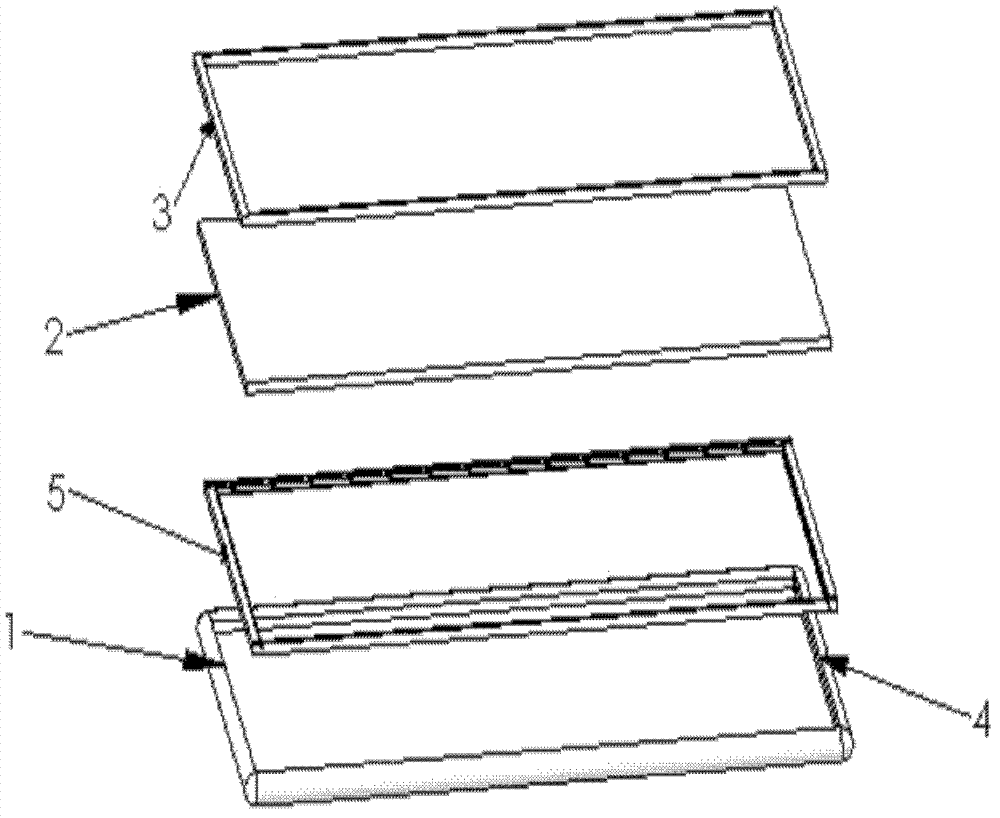
图1为本发明的一种高光效大功率LED面板灯的结构示意图。Fig. 1 is a structural schematic diagram of a high-efficiency high-power LED panel light of the present invention.
图2为本发明的一种高光效大功率LED面板灯的LED灯条安装示意图。Fig. 2 is a schematic diagram of installation of an LED light bar of a high-efficiency high-power LED panel light of the present invention.
图3为本发明的一种高光效大功率LED面板灯德LED芯片封装结构示意图Fig. 3 is a schematic diagram of the packaging structure of a high-efficiency high-power LED panel lamp and an LED chip of the present invention
图4为本发明的一种高光效大功率LED面板灯的光强分布模拟图。Fig. 4 is a simulation diagram of light intensity distribution of a high-efficiency high-power LED panel light of the present invention.
实施方式Implementation
具体实施例一Specific embodiment one
如图1所示,为本发明的一种高光效大功率LED面板灯的整体结构图,该面板灯包括底板1,导光板2,面板3,反射器4,LED灯条5,电源6,采用铝基板压铸成型成面板灯底板1,底板边缘四周有弧形翘曲,使用用真空离子镀膜机在翘曲内表面上镀上一层镜面反射膜构成反射器,使用真空离子镀膜机在底板上镀上一层反射膜,反射膜的反射率由边缘向中部逐渐升高,LED灯条5安装于底板1四周边缘处,将折射率接近LED芯片的掺杂有散射粒子的导光板2安装于底板之上,导光板四周边缘与LED芯片精密贴合,LED芯片与导光板之间采用折射率与导光板相接近的柔性硅胶材料填充粘结,当LED灯条5中发出的光通过发射器4聚焦后射入导光板中,一部分光直接出射,另一部分的光通过底板反射后出射,由于底板所镀反射膜的反射率边缘低中部高,通过合理的设定反射率曲线,可以使面板灯出光表面亮度趋于均匀。As shown in Figure 1, it is an overall structural diagram of a high-efficiency high-power LED panel light of the present invention, which comprises a
如图2所示,为本发明的LED灯条安装示意图,LED芯片11封装于铝基板12之上,LED芯片11中产生的热量通过铝基板传导至底板上,因底板与反射器为一体结构,增大了整体的散热面积。As shown in Figure 2, it is a schematic diagram of the installation of the LED light bar of the present invention. The LED chip 11 is packaged on the
如图3所示,为本发明的LED芯片封装结构示意图,将LED芯片21使用固晶胶粘结于长条型铝基板22上的凹槽中,使用邦定机降LED芯片串联起来,在凹槽中灌入荧光粉封装,各芯片之间采用恒定电流串联驱动。As shown in FIG. 3 , it is a schematic diagram of the LED chip packaging structure of the present invention. The
本实施方式中,采用800*800*5mm的长方形铝合金薄板压制成LED面板灯底板,其中弧形翘曲的翘曲弧度为30度,共使用480颗LED芯片集成封装于四根长条形铝基板上形成灯条,每根灯条中LED芯片采用恒定电流串联驱动。四根灯条分四路采用并联驱动,灯具点亮时导光板表面亮度均匀,光线柔和,看不到明显亮区和暗区,灯具点亮后100小时,灯具表面温度低于50摄氏度。In this embodiment, a rectangular aluminum alloy sheet of 800*800*5mm is used to press the base plate of the LED panel light, and the arc-shaped warping arc is 30 degrees, and a total of 480 LED chips are integrated and packaged in four long strips. Light bars are formed on the aluminum substrate, and the LED chips in each light bar are driven in series with a constant current. The four light strips are divided into four circuits and driven in parallel. When the lamp is lit, the surface brightness of the light guide plate is uniform, the light is soft, and no obvious bright and dark areas can be seen. 100 hours after the lamp is lit, the surface temperature of the lamp is lower than 50 degrees Celsius.
Claims (9)
Priority Applications (1)
| Application Number | Priority Date | Filing Date | Title |
|---|---|---|---|
| CN201110315862XA CN103047553A (en) | 2011-10-17 | 2011-10-17 | High-luminous-efficacy high-power light-emitting diode (LED) panel light |
Applications Claiming Priority (1)
| Application Number | Priority Date | Filing Date | Title |
|---|---|---|---|
| CN201110315862XA CN103047553A (en) | 2011-10-17 | 2011-10-17 | High-luminous-efficacy high-power light-emitting diode (LED) panel light |
Publications (1)
| Publication Number | Publication Date |
|---|---|
| CN103047553A true CN103047553A (en) | 2013-04-17 |
Family
ID=48060307
Family Applications (1)
| Application Number | Title | Priority Date | Filing Date |
|---|---|---|---|
| CN201110315862XA Pending CN103047553A (en) | 2011-10-17 | 2011-10-17 | High-luminous-efficacy high-power light-emitting diode (LED) panel light |
Country Status (1)
| Country | Link |
|---|---|
| CN (1) | CN103047553A (en) |
Cited By (7)
| Publication number | Priority date | Publication date | Assignee | Title |
|---|---|---|---|---|
| WO2017024654A1 (en) * | 2015-08-12 | 2017-02-16 | 深圳市华星光电技术有限公司 | Light guide plate and backlight module |
| CN107345649A (en) * | 2017-07-28 | 2017-11-14 | 江苏欧惠达光电节能科技有限公司 | A kind of anti-explosion panel lamp |
| CN110207035A (en) * | 2018-02-28 | 2019-09-06 | 常熟卓辉光电科技股份有限公司 | A kind of explosion-proof lighting lamp of panel type |
| CN111430516A (en) * | 2020-03-24 | 2020-07-17 | 纳晶科技股份有限公司 | Quantum dot light-emitting device and display device |
| CN113236989A (en) * | 2021-05-11 | 2021-08-10 | 吴远 | Flexible patch lamp strip capable of improving heat dissipation effect |
| CN113432082A (en) * | 2021-06-29 | 2021-09-24 | 傅睿 | Flat reading lamp |
| CN113985656A (en) * | 2021-10-27 | 2022-01-28 | 合肥京东方光电科技有限公司 | Backlight source, backlight module and display device |
Citations (11)
| Publication number | Priority date | Publication date | Assignee | Title |
|---|---|---|---|---|
| CN1448766A (en) * | 2002-04-04 | 2003-10-15 | 精工爱普生株式会社 | Heat radiating component, lighting apparatus, photoelectric apparatus and electronic apparatus |
| CN1740869A (en) * | 2004-12-01 | 2006-03-01 | 友达光电股份有限公司 | flat panel display |
| CN1932619A (en) * | 2005-09-16 | 2007-03-21 | 三星电子株式会社 | Display device |
| CN201297505Y (en) * | 2008-09-27 | 2009-08-26 | 苏州纳科显示技术有限公司 | Portable LED illumination apparatus |
| CN201373281Y (en) * | 2009-02-17 | 2009-12-30 | 深圳市联创健和光电股份有限公司 | Improved LED panel lamp |
| CN101739917A (en) * | 2010-01-27 | 2010-06-16 | 秦厚敬 | Positive light advertising board device |
| CN201507807U (en) * | 2009-08-06 | 2010-06-16 | 陈大庆 | High-efficiency side-light LED energy-saving lighting fixtures |
| JP2010231984A (en) * | 2009-03-26 | 2010-10-14 | Panasonic Electric Works Co Ltd | Display device |
| CN201731330U (en) * | 2010-06-23 | 2011-02-02 | 深圳市普耐光电科技有限公司 | Panel lamp being capable of serving as lamp box |
| US7999887B2 (en) * | 2006-12-21 | 2011-08-16 | Hitachi Displays, Ltd. | Liquid crystal display device |
| CN202361110U (en) * | 2011-10-17 | 2012-08-01 | 中国科学院福建物质结构研究所 | High-power LED panel light with high luminous efficiency |
-
2011
- 2011-10-17 CN CN201110315862XA patent/CN103047553A/en active Pending
Patent Citations (11)
| Publication number | Priority date | Publication date | Assignee | Title |
|---|---|---|---|---|
| CN1448766A (en) * | 2002-04-04 | 2003-10-15 | 精工爱普生株式会社 | Heat radiating component, lighting apparatus, photoelectric apparatus and electronic apparatus |
| CN1740869A (en) * | 2004-12-01 | 2006-03-01 | 友达光电股份有限公司 | flat panel display |
| CN1932619A (en) * | 2005-09-16 | 2007-03-21 | 三星电子株式会社 | Display device |
| US7999887B2 (en) * | 2006-12-21 | 2011-08-16 | Hitachi Displays, Ltd. | Liquid crystal display device |
| CN201297505Y (en) * | 2008-09-27 | 2009-08-26 | 苏州纳科显示技术有限公司 | Portable LED illumination apparatus |
| CN201373281Y (en) * | 2009-02-17 | 2009-12-30 | 深圳市联创健和光电股份有限公司 | Improved LED panel lamp |
| JP2010231984A (en) * | 2009-03-26 | 2010-10-14 | Panasonic Electric Works Co Ltd | Display device |
| CN201507807U (en) * | 2009-08-06 | 2010-06-16 | 陈大庆 | High-efficiency side-light LED energy-saving lighting fixtures |
| CN101739917A (en) * | 2010-01-27 | 2010-06-16 | 秦厚敬 | Positive light advertising board device |
| CN201731330U (en) * | 2010-06-23 | 2011-02-02 | 深圳市普耐光电科技有限公司 | Panel lamp being capable of serving as lamp box |
| CN202361110U (en) * | 2011-10-17 | 2012-08-01 | 中国科学院福建物质结构研究所 | High-power LED panel light with high luminous efficiency |
Cited By (10)
| Publication number | Priority date | Publication date | Assignee | Title |
|---|---|---|---|---|
| WO2017024654A1 (en) * | 2015-08-12 | 2017-02-16 | 深圳市华星光电技术有限公司 | Light guide plate and backlight module |
| CN107345649A (en) * | 2017-07-28 | 2017-11-14 | 江苏欧惠达光电节能科技有限公司 | A kind of anti-explosion panel lamp |
| CN110207035A (en) * | 2018-02-28 | 2019-09-06 | 常熟卓辉光电科技股份有限公司 | A kind of explosion-proof lighting lamp of panel type |
| CN111430516A (en) * | 2020-03-24 | 2020-07-17 | 纳晶科技股份有限公司 | Quantum dot light-emitting device and display device |
| CN111430516B (en) * | 2020-03-24 | 2021-10-22 | 纳晶科技股份有限公司 | Quantum dot light-emitting device and display device |
| CN113236989A (en) * | 2021-05-11 | 2021-08-10 | 吴远 | Flexible patch lamp strip capable of improving heat dissipation effect |
| CN113236989B (en) * | 2021-05-11 | 2023-06-13 | 深圳迪亚士照明科技有限公司 | Flexible patch lamp strip capable of improving heat dissipation effect |
| CN113432082A (en) * | 2021-06-29 | 2021-09-24 | 傅睿 | Flat reading lamp |
| CN113985656A (en) * | 2021-10-27 | 2022-01-28 | 合肥京东方光电科技有限公司 | Backlight source, backlight module and display device |
| CN113985656B (en) * | 2021-10-27 | 2023-12-26 | 合肥京东方光电科技有限公司 | Backlight, backlight module and display device |
Similar Documents
| Publication | Publication Date | Title |
|---|---|---|
| CN101749553B (en) | Packaging module of low-power light emitting diode (LED) luminescent chip | |
| CN101270855A (en) | An LED-based surface light source lighting device | |
| CN101696790A (en) | High-power LED heat-dissipation packaging structure | |
| JP2016518724A (en) | LED module and manufacturing method thereof | |
| CN101551067A (en) | White light LED light source module adopting COB technology and array interconnecting | |
| CN204857783U (en) | A side-emitting LED | |
| CN102222665B (en) | Integrated LED (light emitting diode) module with thin fly's-eye lens | |
| CN2540685Y (en) | High-efficient high power light-emitting diode | |
| CN203641916U (en) | Fluorescent LED device | |
| CN102364709A (en) | High-power LED packaging structure | |
| CN206943847U (en) | A kind of LED that can quickly assemble | |
| CN202361110U (en) | High-power LED panel light with high luminous efficiency | |
| Chan | Electronic packaging for solid-state lighting | |
| CN202633295U (en) | LED support, LED area light source and LED lamp | |
| CN103227266B (en) | LED encapsulation structure | |
| CN209544349U (en) | An LED lighting module for long-distance visible light communication | |
| CN212226734U (en) | Lamp capable of realizing rectangular uniform illumination and lamp set | |
| CN106229311A (en) | A kind of production technology of LED light emitting diode | |
| CN106486578A (en) | A kind of mirror-surface aluminum base board fluorescent tube | |
| CN202024127U (en) | Combined type light-emitting diode (LED) module | |
| CN108281416A (en) | A kind of direct-injection type light source | |
| CN220688807U (en) | Efficient energy-saving LED illuminating lamp | |
| CN217899570U (en) | High-brightness LED lamp bead for LED lighting facility | |
| CN208706676U (en) | A kind of light emitting diode with scatter-type light-emitting surface | |
| CN100570213C (en) | LED Lighting Module |
Legal Events
| Date | Code | Title | Description |
|---|---|---|---|
| C06 | Publication | ||
| PB01 | Publication | ||
| C10 | Entry into substantive examination | ||
| SE01 | Entry into force of request for substantive examination | ||
| C02 | Deemed withdrawal of patent application after publication (patent law 2001) | ||
| WD01 | Invention patent application deemed withdrawn after publication |
Application publication date: 20130417 |