CN102214895A - Semiconductor device and method for manufacturing the same - Google Patents
Semiconductor device and method for manufacturing the same Download PDFInfo
- Publication number
- CN102214895A CN102214895A CN2011100850197A CN201110085019A CN102214895A CN 102214895 A CN102214895 A CN 102214895A CN 2011100850197 A CN2011100850197 A CN 2011100850197A CN 201110085019 A CN201110085019 A CN 201110085019A CN 102214895 A CN102214895 A CN 102214895A
- Authority
- CN
- China
- Prior art keywords
- scolder
- electrode
- semiconductor
- secondary fixture
- semiconductor laser
- Prior art date
- Legal status (The legal status is an assumption and is not a legal conclusion. Google has not performed a legal analysis and makes no representation as to the accuracy of the status listed.)
- Pending
Links
Images


Classifications
-
- H—ELECTRICITY
- H01—ELECTRIC ELEMENTS
- H01S—DEVICES USING THE PROCESS OF LIGHT AMPLIFICATION BY STIMULATED EMISSION OF RADIATION [LASER] TO AMPLIFY OR GENERATE LIGHT; DEVICES USING STIMULATED EMISSION OF ELECTROMAGNETIC RADIATION IN WAVE RANGES OTHER THAN OPTICAL
- H01S5/00—Semiconductor lasers
- H01S5/02—Structural details or components not essential to laser action
- H01S5/022—Mountings; Housings
- H01S5/0233—Mounting configuration of laser chips
- H01S5/0234—Up-side down mountings, e.g. Flip-chip, epi-side down mountings or junction down mountings
-
- H—ELECTRICITY
- H01—ELECTRIC ELEMENTS
- H01L—SEMICONDUCTOR DEVICES NOT COVERED BY CLASS H10
- H01L24/00—Arrangements for connecting or disconnecting semiconductor or solid-state bodies; Methods or apparatus related thereto
- H01L24/01—Means for bonding being attached to, or being formed on, the surface to be connected, e.g. chip-to-package, die-attach, "first-level" interconnects; Manufacturing methods related thereto
- H01L24/26—Layer connectors, e.g. plate connectors, solder or adhesive layers; Manufacturing methods related thereto
- H01L24/31—Structure, shape, material or disposition of the layer connectors after the connecting process
- H01L24/32—Structure, shape, material or disposition of the layer connectors after the connecting process of an individual layer connector
-
- H—ELECTRICITY
- H01—ELECTRIC ELEMENTS
- H01L—SEMICONDUCTOR DEVICES NOT COVERED BY CLASS H10
- H01L24/00—Arrangements for connecting or disconnecting semiconductor or solid-state bodies; Methods or apparatus related thereto
- H01L24/80—Methods for connecting semiconductor or other solid state bodies using means for bonding being attached to, or being formed on, the surface to be connected
- H01L24/83—Methods for connecting semiconductor or other solid state bodies using means for bonding being attached to, or being formed on, the surface to be connected using a layer connector
-
- H—ELECTRICITY
- H01—ELECTRIC ELEMENTS
- H01S—DEVICES USING THE PROCESS OF LIGHT AMPLIFICATION BY STIMULATED EMISSION OF RADIATION [LASER] TO AMPLIFY OR GENERATE LIGHT; DEVICES USING STIMULATED EMISSION OF ELECTROMAGNETIC RADIATION IN WAVE RANGES OTHER THAN OPTICAL
- H01S5/00—Semiconductor lasers
- H01S5/02—Structural details or components not essential to laser action
- H01S5/022—Mountings; Housings
- H01S5/0235—Method for mounting laser chips
- H01S5/02355—Fixing laser chips on mounts
- H01S5/0237—Fixing laser chips on mounts by soldering
-
- H—ELECTRICITY
- H01—ELECTRIC ELEMENTS
- H01L—SEMICONDUCTOR DEVICES NOT COVERED BY CLASS H10
- H01L2224/00—Indexing scheme for arrangements for connecting or disconnecting semiconductor or solid-state bodies and methods related thereto as covered by H01L24/00
- H01L2224/01—Means for bonding being attached to, or being formed on, the surface to be connected, e.g. chip-to-package, die-attach, "first-level" interconnects; Manufacturing methods related thereto
- H01L2224/26—Layer connectors, e.g. plate connectors, solder or adhesive layers; Manufacturing methods related thereto
- H01L2224/31—Structure, shape, material or disposition of the layer connectors after the connecting process
- H01L2224/32—Structure, shape, material or disposition of the layer connectors after the connecting process of an individual layer connector
- H01L2224/325—Material
- H01L2224/32505—Material outside the bonding interface, e.g. in the bulk of the layer connector
- H01L2224/32507—Material outside the bonding interface, e.g. in the bulk of the layer connector comprising an intermetallic compound
-
- H—ELECTRICITY
- H01—ELECTRIC ELEMENTS
- H01L—SEMICONDUCTOR DEVICES NOT COVERED BY CLASS H10
- H01L2224/00—Indexing scheme for arrangements for connecting or disconnecting semiconductor or solid-state bodies and methods related thereto as covered by H01L24/00
- H01L2224/80—Methods for connecting semiconductor or other solid state bodies using means for bonding being attached to, or being formed on, the surface to be connected
- H01L2224/83—Methods for connecting semiconductor or other solid state bodies using means for bonding being attached to, or being formed on, the surface to be connected using a layer connector
- H01L2224/8338—Bonding interfaces outside the semiconductor or solid-state body
- H01L2224/83385—Shape, e.g. interlocking features
-
- H—ELECTRICITY
- H01—ELECTRIC ELEMENTS
- H01L—SEMICONDUCTOR DEVICES NOT COVERED BY CLASS H10
- H01L2924/00—Indexing scheme for arrangements or methods for connecting or disconnecting semiconductor or solid-state bodies as covered by H01L24/00
- H01L2924/013—Alloys
- H01L2924/0132—Binary Alloys
- H01L2924/01322—Eutectic Alloys, i.e. obtained by a liquid transforming into two solid phases
-
- H—ELECTRICITY
- H01—ELECTRIC ELEMENTS
- H01S—DEVICES USING THE PROCESS OF LIGHT AMPLIFICATION BY STIMULATED EMISSION OF RADIATION [LASER] TO AMPLIFY OR GENERATE LIGHT; DEVICES USING STIMULATED EMISSION OF ELECTROMAGNETIC RADIATION IN WAVE RANGES OTHER THAN OPTICAL
- H01S5/00—Semiconductor lasers
- H01S5/02—Structural details or components not essential to laser action
- H01S5/0201—Separation of the wafer into individual elements, e.g. by dicing, cleaving, etching or directly during growth
- H01S5/0202—Cleaving
-
- H—ELECTRICITY
- H01—ELECTRIC ELEMENTS
- H01S—DEVICES USING THE PROCESS OF LIGHT AMPLIFICATION BY STIMULATED EMISSION OF RADIATION [LASER] TO AMPLIFY OR GENERATE LIGHT; DEVICES USING STIMULATED EMISSION OF ELECTROMAGNETIC RADIATION IN WAVE RANGES OTHER THAN OPTICAL
- H01S5/00—Semiconductor lasers
- H01S5/30—Structure or shape of the active region; Materials used for the active region
- H01S5/32—Structure or shape of the active region; Materials used for the active region comprising PN junctions, e.g. hetero- or double- heterostructures
- H01S5/323—Structure or shape of the active region; Materials used for the active region comprising PN junctions, e.g. hetero- or double- heterostructures in AIIIBV compounds, e.g. AlGaAs-laser, InP-based laser
- H01S5/32308—Structure or shape of the active region; Materials used for the active region comprising PN junctions, e.g. hetero- or double- heterostructures in AIIIBV compounds, e.g. AlGaAs-laser, InP-based laser emitting light at a wavelength less than 900 nm
- H01S5/32341—Structure or shape of the active region; Materials used for the active region comprising PN junctions, e.g. hetero- or double- heterostructures in AIIIBV compounds, e.g. AlGaAs-laser, InP-based laser emitting light at a wavelength less than 900 nm blue laser based on GaN or GaP
Abstract
The invention relates to a semiconductor device having a high heat radiation and yield and a method for manufacturing the same. A semiconductor laser 1 is mounted on the submount 12 via a solder 11 in a junction-down manner. The semiconductor laser 1 has an n-type GaN substrate 2; a semiconductor laminated structure 3 containing a p-n junction and formed on an n-type GaN substrate 2; and an electrode 8 formed on the semiconductor laminated structure 3. The electrode 8 is combined on the submount 12 via the solder 11. A high-melting-point metal film 10 is placed around the electrode between the submount 12 and the semiconductor laminated structure 3.
Description
Technical field
The present invention relates on secondary fixture across scolder to tie semiconductor device and the manufacture method thereof that downward mode is equipped with semiconductor laser, particularly can guarantee high thermal diffusivity and improve the semiconductor device and the manufacture method thereof of rate of finished products.
Background technology
Semiconductor laser is installed on the secondary fixture to tie the mode of making progress or to tie downward mode across scolder.In order reducing cost, under the situation that makes the chip reduced width, at knot upwards in the mode, not avoid luminous striped and carry out the space of wire-bonded.Therefore, the general knot downward mode (for example, with reference to patent documentation 1) that adopts.In addition, because the thermal diffusivity of the downward mode of knot is good, so, can improve the characteristic under high power or the high temperature.
Patent documentation 1: Japanese kokai publication hei 5-110203 communique.
Utilize the punching press when installing, scolder is expanded laterally, in laterally exposing of chip, along the side protuberance of chip.Adopting under the situation of tying the mode of making progress, leaving the distance of the pn knot from the installed surface to the semiconductor laser, so, there be not the situation of pn knot because of the scolder short circuit.But under the situation that adopts the downward mode of knot, pn ties because of the scolder short circuit, has this problem of decrease in yield.
In addition, in GaN based semiconductor laser device, rate of crystalline growth is slow or reduce fire damage to active layer, so the upper caldding layer on the active layer or the aggregate thickness of contact layer are generally less than 1 μ m.These aggregate thickness 3 μ m~5 μ m than GaAs based semiconductor laser device etc. are thin.Therefore, under the situation of GaN based semiconductor laser device, the distance of knot is shorter from the installed surface to pn, so the problems referred to above are remarkable especially.
In addition, consider surround with dielectric film between secondary fixture and the semiconductor laser electrode around, to prevent that scolder is around the side to semiconductor laser.But, because the thermal diffusivity of dielectric film is low, so, can not be in the heat that light-emitting zone produced of semiconductor laser fully to secondary fixture heat radiation.
Summary of the invention
The present invention proposes in order to solve above-mentioned problem, and its purpose is to obtain guaranteeing the semiconductor device and the manufacture method thereof of high thermal diffusivity and raising rate of finished products.
The invention provides a kind of semiconductor device, it is characterized in that, possess secondary fixture and be installed in semiconductor laser on the described secondary fixture to tie downward mode across scolder, described semiconductor laser has Semiconductor substrate, be formed on the described Semiconductor substrate and contain the semiconductor stacked structure of pn knot and the electrode that on described semiconductor stacked structure, forms, described electrode across described solder bonds on described secondary fixture, between described secondary fixture and described semiconductor stacked structure, dispose high melting point metal film or high-melting-point dielectric film in the mode on every side of surrounding described electrode.
According to the present invention, can guarantee high thermal diffusivity and can improve rate of finished products.
Description of drawings
Fig. 1 is the profile of the semiconductor laser of expression execution mode 1.
Fig. 2 is the profile of the semiconductor device of expression execution mode 1.
Fig. 3 is the profile of the semiconductor device of expression execution mode 2.
Fig. 4 is the profile of the semiconductor device of expression execution mode 3.
Fig. 5 is the profile of manufacture method that is used to illustrate the semiconductor device of execution mode 3.
Fig. 6 is the binary system phase diagram of AuSn.
Fig. 7 is the profile of variation of manufacture method that is used to illustrate the semiconductor device of execution mode 3.
Fig. 8 is the profile of the semiconductor device of expression execution mode 4.
Fig. 9 is the profile of manufacture method that is used to illustrate the semiconductor device of execution mode 4.
Figure 10 is the profile of the semiconductor device of expression execution mode 5.
Figure 11 is the profile of manufacture method that is used to illustrate the semiconductor device of execution mode 5.
Figure 12 is the binary system phase diagram of SnAg.
Figure 13 is the profile of variation that is used to illustrate the semiconductor device of execution mode 5.
Figure 14 is the profile of the semiconductor device of expression execution mode 6.
Figure 15 is the profile of manufacture method that is used to illustrate the semiconductor device of execution mode 6.
Figure 16 is the profile of variation of the semiconductor device of expression execution mode 6.
Figure 17 is the plane graph of manufacture method of the semiconductor device of expression execution mode 7.
Figure 18 is the profile of manufacture method of the semiconductor device of expression execution mode 7.
Figure 19 is the amplification profile with the part of dotted line among Figure 18.
Figure 20 is the amplification profile of variation of manufacture method of the semiconductor device of expression execution mode 7.
Description of reference numerals:
1 semiconductor laser
2 n type GaN substrates (Semiconductor substrate)
3 semiconductor stacked structures
8 electrodes
10 high melting point metal films
11 scolders
12 secondary fixtures
14,20,26,27 grooves
15 metal pads
16 first alloy-layers
17 second alloy-layers
18 engaging zones
19,21 Au films (metal level)
24 intermetallic compounds
25 induced materials (attractive material)
28 high resistance zones
29 dielectric films.
Embodiment
Describe with reference to the semiconductor device of accompanying drawing embodiments of the present invention.The identical Reference numeral of structural element mark to identical omits repeat specification sometimes.
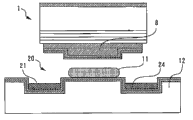
Fig. 1 is the profile of the semiconductor laser 1 of expression execution mode 1.In n type GaN substrate 2(Semiconductor substrate) on be formed with the semiconductor stacked structure 3 that contains pn knot.Semiconductor stacked structure 3 has n type AlGaN cover layer 4, InGaN active layer 5, p type AlGaN cover layer 6 and the p type GaN contact layer 7 that stacks gradually from n type GaN substrate 2 sides.On p type GaN contact layer 7, be formed with electrode 8, be formed with electrode 9 at the lower surface of n type GaN substrate 2.In electrode 8,9, contain gold (Au).
Dispose high melting point metal film 10 in the mode on every side of surrounding electrode 8.High melting point metal film 10 is made of platinum (Pt), nickel (Ni), nichrome (NiCr), tungsten (W), titanium (Ti), tungsten titanium (TiW), molybdenum (Mo), tantalum (Ta) or niobium (Nb).And, replace high melting point metal film 10, adopt by the oxide-film of each material of above-mentioned high melting point metal film 10 or high-melting-point dielectric film that nitride film constitutes also passable.
Fig. 2 is the profile of the semiconductor device of expression execution mode 1.Semiconductor laser 1 is installed on the secondary fixture 12 across scolder 11 to tie downward mode.The electrode 8 of semiconductor laser 1 is bonded on the secondary fixture 12 across scolder 11.Scolder 11 is made of the material of the alloy that forms AuSn class, SnAg class, SnAgCu class, Sn-Zn class, Sn-Bi class, PbSn class, AuSi class, AuGe class.
As described above, in the present embodiment, between secondary fixture 12 and semiconductor stacked structure 3, dispose high melting point metal film 10 or high-melting-point dielectric film in the mode on every side of surrounding electrode 8.Utilize this high melting point metal film 10 or high-melting-point dielectric film can prevent scolder 11 around causing the short circuit of pn knot to the side of semiconductor laser 1, so, rate of finished products is improved.
In addition, for high melting point metal film 10 or high-melting-point dielectric film, thermal conductivity is higher about 10 times than dielectric film.The thermal conductivity of refractory metal is 50~200W/mK, with respect to this, as the SiO of general dielectric film
2Thermal conductivity be below the 10W/mK, the thermal conductivity of SiN is below the 20W/mK.
The heat that is produced at the light-emitting zone 13 of semiconductor laser 1 via electrode 8, high melting point metal film 10 and scolder 11 to secondary fixture 12 heat radiations.Shown in present embodiment, like that, surrounding with high melting point metal film 10 and high-melting-point dielectric film under the situation on every side of electrode 8, comparing, can guarantee high thermal diffusivity with the situation on every side of surrounding electrode 8 with dielectric film.Particularly, be favourable to requiring high-power semiconductor laser more than hundreds of mW or operating current, the higher semiconductor laser of voltage.
Fig. 3 is the profile of the semiconductor device of expression execution mode 2.In semiconductor stacked structure 3, be formed with groove 14 in the mode on every side of surrounding electrode 8.High melting point metal film 10 or high-melting-point dielectric film cover the inside of this groove 14.But high melting point metal film 10 does not carry out ohm with semiconductor stacked structure 13 and engages.Other structures are identical with execution mode 1.
When mounted, can make unnecessary scolder 11 flow into the inside of groove 14.Therefore, can prevent scolder 11 around making the short circuit of pn knot to the side of semiconductor laser 1, so, rate of finished products is improved.
The width of groove 14 is below the 30 μ m, is preferably 5~20 μ m.About depth ratio pn junction depth 1~10 μ m of groove 14.Thus, can increase the volume of the groove 14 that flows into unnecessary scolder 11.
In addition, for the position of groove 14, be inboard, preferably apart from the inboard of end 5~20 μ m of semiconductor laser 1 apart from end 5~30 μ m of semiconductor laser 1.Thus, make groove 14 near the chip ends, therefore, even with the reduced width of semiconductor laser 1 to below the 150 μ m for example under the situation about 100 μ m, can make also that to engage width bigger, can guarantee adhesive strength.
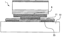
Fig. 4 is the profile of the semiconductor device of expression execution mode 3.The high melting point metal film 10 that replaces execution mode 1 between secondary fixture 12 and semiconductor stacked structure 3, disposes metal pad 15 in the mode on every side of surrounding electrode 8.In metal pad 15, contain gold (Au).Scolder 11 is AuSn that the Sn by the Au of 80wt% and 20wt% constitutes.The fusing point of this scolder 11 is 280 ℃.
Fig. 5 is the profile of manufacture method that is used to illustrate the semiconductor device of execution mode 3.At first, prepare to contain the semiconductor laser 1 of pn knot.Mode with around the electrode 8 that surrounds semiconductor laser 1 forms metal pad 15 on semiconductor laser 1.On secondary fixture 12, form scolder 11.Afterwards, semiconductor laser 1 is installed on the secondary fixture 12 across scolder 11 to tie downward mode.Installation temperature when being installed in semiconductor laser 1 on the secondary fixture 12 is about 300~350 ℃.This installs the fusing point height of temperature than scolder 11.
When this was installed, as shown in Figure 4, the Au of the constituent material of electrode 8 spread in scolder 11, forms first alloy-layer 16.Fig. 6 is the binary system phase diagram of AuSn.As shown in Figure 6, the Au amount is many more, and the fusing point of AuSn is high more.Therefore, the fusing point of first alloy-layer 16 is than the fusing point height of scolder 11.
If first alloy-layer 16 reaches metal pad 15, then the Au of the constituent material of metal pad 15 spreads in first alloy-layer 16, forms second alloy-layer 17.Second alloy-layer 17 is made of the Au of for example 85wt% and the Sn of 15wt%.The fusing point of this second alloy-layer 17 rises to about 400 ℃.Therefore, the fusing point of second alloy-layer 17 so scolder 11 reaches metal pad 15, become second alloy-layer 17, thereby the fusion of scolder 11 stops than temperature (about 300~350 ℃) height is installed.Therefore, can prevent scolder 11 around making the short circuit of pn knot to the side of semiconductor laser 1, so, rate of finished products is improved.
In addition, set the thickness of metal pad 15 as follows: the volume in the space that is surrounded by secondary fixture 12, semiconductor stacked structure 3, metal pad 15 and scolder 11 alloyings volume afterwards are about equally.Specifically, make the thickness of metal pad 15 thin thickness a few percent to percent about 30 than the scolder 11 of Fig. 5.
In addition, for the AuSn scolder, fusing point also rises under the situation that the composition of Sn uprises, so, as constituent material, also can adopt the metal pad 15 that contains Sn.In this case, for example, if second alloy-layer 17 is the Au of 70wt% and the Sn of 30wt%, then its fusing point is about 390 ℃.Therefore, can access identical effect.
In addition, scolder 11 is not limited to AuSn, also can be to form SnAg class, SnAgCu class, Sn-Zn class, Sn-Bi class, PbSn class, AuSi class or the alloy of AuGe class and the material that fusing point changes according to ratio of components.And, as the material of metal pad 15, can adopt the material that comprises following material: when carrying out alloying or being added in the scolder 11, the fusing point of scolder 11 is risen with scolder 11.Therefore, can access identical effect.
Fig. 7 is the profile of variation of manufacture method that is used to illustrate the semiconductor device of execution mode 3.In above-mentioned example, on semiconductor laser 1, formed metal pad 15, still, in this variation,, form metal pad 15 to surround the mode of the engaging zones 18 on the secondary fixture 12.And the engaging zones 18 on secondary fixture 12 forms scolder 11.Afterwards, semiconductor laser 1 is installed in engaging zones 18 on the secondary fixture 12 across scolder 11 to tie downward mode.Other operations are identical with above-mentioned example, can access identical effect.
Execution mode 4
Fig. 8 is the profile of the semiconductor device of expression execution mode 4.The high melting point metal film 10 that replaces execution mode 1 between secondary fixture 12 and electrode 8, disposes Au film 19(metal film in the periphery of electrode 8).Scolder 11 is AuSn that the Sn by the Au of 80wt% and 20wt% constitutes.The fusing point of this scolder 11 is 280 ℃.
Fig. 9 is the profile of manufacture method that is used to illustrate the semiconductor device of execution mode 4.At first, prepare to contain the semiconductor laser 1 of pn knot.And, form Au film 19 in the periphery of the electrode 8 of semiconductor laser 1.On electrode 8 by Au film 19 area surrounded evaporation scolders 11.Afterwards, semiconductor laser 1 is installed on the secondary fixture 12 to tie downward mode across scolder 11.Installation temperature when being installed in semiconductor laser 1 on the secondary fixture 12 is about 300~350 ℃.This installs the fusing point height of temperature than scolder 11.
When this was installed, as shown in Figure 8, the Au of the constituent material of electrode 8 spread in scolder 11, forms first alloy-layer 16.If first alloy-layer 16 reaches Au film 19, then the Au of the constituent material of Au film 19 spreads in first alloy-layer 16, forms second alloy-layer 17.Second alloy-layer 17 is made of the Au of for example 85wt% and the Sn of 15wt%.The fusing point of this second alloy-layer 17 rises to about 400 ℃.Therefore, the fusing point of second alloy-layer 17 so scolder 11 reaches Au film 19, become second alloy-layer 17, thereby the fusion of scolder 11 stops than temperature (about 300~350 ℃) height is installed.Therefore, can prevent scolder 11 around making the short circuit of pn knot to the side of semiconductor laser 1, so, rate of finished products is improved.
In addition, set the thickness of Au film 19 as follows: carried out alloying volume afterwards about equally by the volume in the space of secondary fixture 12, electrode 8 and 19 encirclements of Au film and scolder 11.Specifically, make the thickness of Au film 19 thin thickness a few percent to percent about 30 than the scolder 11 of Fig. 9.
Execution mode 5
Figure 10 is the profile of the semiconductor device of expression execution mode 5.The high melting point metal film 10 that replaces execution mode 1 is formed with groove 20 in the mode on every side of surrounding electrode 8 on secondary fixture 12.In groove 20, be formed with Au layer 21(metal level).Scolder 11 is SnAg.On electrode 8 and secondary fixture 12, be formed with Au coating 22 and Pt/ burr (flash) Au layer 23.
Figure 11 is the profile of manufacture method that is used to illustrate the semiconductor device of execution mode 5.At first, prepare to contain the semiconductor laser 1 of pn knot.Then, form groove 20, in groove 20, form Au layer 21 in the mode of surrounding the engaging zones 18 on the secondary fixture 12.And the engaging zones 18 on secondary fixture 12 forms scolder 11.Afterwards, semiconductor laser 1 is installed to engaging zones 18 on the secondary fixture 12 to tie downward mode across scolder 11.Installation temperature when being installed to semiconductor laser 1 on the secondary fixture 12 is about 300~350 ℃.This installs the fusing point height of temperature than scolder 11.
When this was installed, scolder 11 flow into the groove 20 of secondary fixture 12.Thus, as shown in figure 10, the Au of the constituent material of Au layer 21 spreads in scolder 11, forms intermetallic compound 24.Intermetallic compound 24 is made of AuSn.The fusing point that contains the scolder 11 of this intermetallic compound 24 rises to for example 380 ℃, than temperature (about 300~350 ℃) height is installed.Thus, because the fusion of scolder 11 stops, so, the expansion of the transverse direction of the scolder 11 in can restrain tank 20.Therefore, can prevent scolder 11 around making the short circuit of pn knot to the side of semiconductor laser 1, so, rate of finished products is improved.
In addition, Figure 12 is the binary system phase diagram of SnAg.For the fusing point of SnAg, be that (eutectic point) is 221 ℃ under 3.5% the situation at Ag, lower, if increasing, Ag then uprises.Therefore, replace Au layer 21 in groove 20, also can access identical effect even the Ag layer is set.In addition, identical with execution mode 3,4, replace the SnAg scolder, adopt the AuSn scolder, Au layer 21 or Sn layer are set in groove 20, identical effect is also arranged.And,, also can access identical effect even make other impurity materials of the fusing point rising of scolder 11 replace Au layer 21 when in groove 20, being provided with when being blended into scolder 11 in.
Figure 13 is the profile of variation that is used to illustrate the semiconductor device of execution mode 5.Au layer 21 is not arranged in the groove 20 of secondary fixture 12, but is arranged on semiconductor laser 1 side in the mode on every side of surrounding electrode 8.In this case, also can access identical effect.In addition, as if in the groove 20 that Au layer 21 is arranged on secondary fixture 12 and on these two positions of semiconductor laser 1 side, then more effective.
Execution mode 6
Figure 14 is the profile of the semiconductor device of expression execution mode 6.The high melting point metal film 10 that replaces execution mode 1 forms groove 20 in the mode on every side of surrounding electrode 8 on secondary fixture 12.Side in the inboard of groove 20 is formed with induced material 25.Induced material 25 is the materials that make the flowability raising of scolder 11.Specifically, induced material 25 is the material identical with scolder 11, constitute, the scolder welding agent (flux) of scolder 11 or the metal material that fusing point descends when carrying out alloying with scolder 11.
Specifically, the scolder welding agent is borax (the 4 Boratex Na that have the character of metal oxide fusion
2B
4O
5(OH)
48H
2O) or zinc chloride (ZnCl
2) aqueous solution etc.For the metal material that fusing point is descended, specifically, be Ag, be Bi, be In, be Ag, Al, Ga etc. for the Sn-9Zn scolder for the Sn-Ag scolder for the Sn-Ag-Bi-Cu scolder for the Sn-Cu scolder.With respect to Sn-0.75Cu scolder (fusing point is 227 ℃), the fusing point that has added the Sn-3.5Ag-0.75Cu of Ag is 217 ℃.With respect to Sn-2.5Ag-1.0Bi-0.5Cu scolder (fusing point is 214 ℃), the fusing point of the Sn-2.0Ag-3.0Bi-0.75Cu that the amount of Bi is big is 207 ℃.
Figure 15 is the profile of manufacture method that is used to illustrate the semiconductor device of execution mode 6.At first, prepare to contain the semiconductor laser 1 of pn knot.Then, form groove 20, form induced material 25 in the side of the inboard of groove 20 in the mode of surrounding the engaging zones 18 on the secondary fixture 12.And the engaging zones 18 on secondary fixture 12 forms scolder 11.Afterwards, semiconductor laser 1 is installed to engaging zones 18 on the secondary fixture 12 to tie downward mode across scolder 11.
When this was installed, when induced material 25 was blended in the scolder 11, the flowability of scolder 11 improved.Thus, scolder 11 flow in the groove 20 easily.Therefore, can prevent scolder 11 around making the short circuit of pn knot to the side of semiconductor laser 1, so, rate of finished products is improved.In addition, the thickness of induced material 25 is thin more, and unnecessary scolder 11 is easy more to be flow in the groove 20.And the area of induced material 25 is big more, can induce more scolder 11 more.
Figure 16 is the profile of variation of the semiconductor device of expression execution mode 6.On secondary fixture 12, do not form groove 20.On smooth secondary fixture 12, be formed with the induced material 25 that makes scolder 11 fusions easily in the mode on every side of surrounding electrode 8.In this case, scolder 11 expansion in the horizontal on secondary fixture 12 easily owing to induced material 25, scolder 11 does not swell, so, can access identical effect.
Execution mode 7
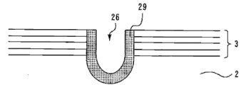
Figure 17 is the plane graph of manufacture method of the semiconductor device of expression execution mode 7.Figure 18 is its profile.Figure 19 is the amplification profile with the part of dotted line among Figure 18.
At first, on the n of wafer-like type GaN substrate 2, form and have the semiconductor stacked structure 3 that comprises the pn knot and a plurality of semiconductor lasers 1 of the electrode 8 on the semiconductor stacked structure 3.
Then,, utilize laser cutting that adjacent semiconductor laser 1 border is each other cut, form groove 26,27 than pn junction depth as Figure 17 and shown in Figure 180.In addition, specifically, before forming groove 26,27, coating photoresist (not shown), the photoresist that utilizes composition will form the part of groove 26,27 is removed.In addition, because the light-emitting zone 13 of semiconductor laser 1 need expose cleavage surface, so the groove 27 that cleavage is used forms in the mode of avoiding light-emitting zone 13.
Then, as shown in figure 19,, utilize and carry out the high resistance processing, form high resistance zone 28 as the long heat treated thermal oxidation method of high temperature on the surface, inside of groove 26,27.Afterwards, remove photoresist.Under the situation of GaN class material, for the surface, inside of groove 26,27, the nitrogen on GaN surface becomes rich Ga state owing to laser cutting is escaped.Therefore, utilize thermal oxidation method to become GaO, can carry out high resistanceization easily.In addition, as the high resistance processing, also can inject the H(proton), the ion of the ion of F, O, Fe, Zn, Si etc. injects.
Then, carry out cleavage etc., be separated into each semiconductor laser 1 along groove 26,27.And, across scolder 11 semiconductor laser 1 is installed on the secondary fixture 12 to tie downward mode.
As described above such, carry out the high resistance processing on the surface, inside of groove 26,27, so, be formed with high resistance zone 28 in the side of semiconductor laser 1.Therefore, even scolder 11 around reach the pn knot to the side of semiconductor laser 1, also can prevent the short circuit of pn knot, so, rate of finished products is improved.
In addition, usually, use the coating protection cleavage surface, so the pn knot does not expose.Therefore, also can not carry out above-mentioned high resistance processing.In addition, the two has used laser cutting groove that separatory groove 26 and cleavage are used 27, still, also can only use laser cutting to separatory groove 26.
In addition, laser cutting is compared with the pin cutting, and superior aspect microfabrication, operating speed is fast.Even compare with etching phase, also superior aspect machining control, therefore can cut deeplyer.Particularly, in the semiconductor laser of GaN class, there is not suitable etching liquid, the wet etching difficulty, so, need laser cutting or dry etching.
Figure 20 is the amplification profile of variation of manufacture method of the semiconductor device of expression execution mode 7.In above-mentioned example, carried out the high resistance processing on the surface, inside of groove 26,27, still, in variation, in groove 26,27, form dielectric film 29.Thus, can access identical effect.
Claims (13)
1. semiconductor device is characterized in that possessing:
Secondary fixture; And
Semiconductor laser utilizes scolder to be installed on the described secondary fixture to tie downward mode,
Described semiconductor laser has: Semiconductor substrate; Semiconductor stacked structure is formed on the described Semiconductor substrate and contains pn and ties; Electrode is formed on the described semiconductor stacked structure,
Described electrode across described solder bonds on described secondary fixture,
Between described secondary fixture and described semiconductor stacked structure, dispose high melting point metal film or high-melting-point dielectric film in the mode on every side of surrounding described electrode.
2. semiconductor device as claimed in claim 1 is characterized in that,
On described semiconductor stacked structure, be formed with groove in the mode on every side of surrounding described electrode,
Described high melting point metal film or described high-melting-point dielectric film cover the inside of described groove,
Described high melting point metal film does not carry out ohm with described semiconductor stacked structure and engages.
3. semiconductor device is characterized in that possessing:
Secondary fixture; And
Semiconductor laser is installed on the described secondary fixture to tie downward mode across scolder,
Described semiconductor laser has: Semiconductor substrate; Semiconductor stacked structure is formed on the described Semiconductor substrate and contains pn and ties; Electrode is formed on the described semiconductor stacked structure,
Described electrode across described solder bonds on described secondary fixture,
Between described secondary fixture and described semiconductor stacked structure, dispose metal pad in the mode on every side of surrounding described electrode,
The constituent material of described electrode is diffused in the described scolder, forms first alloy-layer,
The constituent material of described metal pad is diffused in described first alloy-layer, forms second alloy-layer,
The fusing point of described second alloy-layer is than the fusing point height of described scolder.
4. semiconductor device is characterized in that possessing:
Secondary fixture; And
Semiconductor laser is installed on the described secondary fixture to tie downward mode across scolder,
Described semiconductor laser has: Semiconductor substrate; Semiconductor stacked structure is formed on the described Semiconductor substrate and contains pn and ties; Electrode is formed on the described semiconductor stacked structure,
Described electrode across described solder bonds on described secondary fixture,
Between described secondary fixture and described electrode, dispose metal film in the periphery of described electrode,
The constituent material of described electrode is diffused in the described scolder, forms first alloy-layer,
The constituent material of described metal film is diffused in described first alloy-layer, forms second alloy-layer,
The fusing point of described second alloy-layer is than the fusing point height of described scolder.
5. semiconductor device is characterized in that possessing:
Secondary fixture; And
Semiconductor laser is installed on the described secondary fixture to tie downward mode across scolder,
Described semiconductor laser has: Semiconductor substrate; Semiconductor stacked structure is formed on the described Semiconductor substrate and contains pn and ties; Electrode is formed on the described semiconductor stacked structure,
Described electrode across described solder bonds on described secondary fixture,
On described secondary fixture, be formed with groove in the mode on every side of surrounding described electrode,
In described groove, be formed with metal level,
Spread in the described scolder of the constituent material of described metal level in flowing into described groove, form intermetallic compound,
The fusing point of described intermetallic compound is than the fusing point height of described scolder.
6. semiconductor device is characterized in that possessing:
Secondary fixture; And
Semiconductor laser is installed on the described secondary fixture to tie downward mode across scolder,
Described semiconductor laser has: Semiconductor substrate; Semiconductor stacked structure is formed on the described Semiconductor substrate and contains pn and ties; Electrode is formed on the described semiconductor stacked structure,
Described electrode across described solder bonds on described secondary fixture,
On described secondary fixture, be formed with the induced material of the flowability raising that makes described scolder in the mode on every side of surrounding described electrode.
7. semiconductor device as claimed in claim 6 is characterized in that,
Described induced material is constitute, the scolder welding agent of the material identical with described scolder, described scolder or the metal material that fusing point descends when carrying out alloying with described scolder.
8. as claim 6 or the described semiconductor device of claim 7, it is characterized in that,
On described secondary fixture, be formed with groove in the mode on every side of surrounding described electrode,
Side in the inboard of described groove is formed with described induced material.
9. the manufacture method of a semiconductor device is characterized in that, possesses:
Prepare the operation of semiconductor laser, described semiconductor laser has Semiconductor substrate, be formed on the described Semiconductor substrate and contain the semiconductor stacked structure of pn knot and be formed on electrode on the described semiconductor stacked structure;
On secondary fixture, form the operation of scolder;
On described semiconductor laser, form the operation of metal pad in the mode on every side of surrounding described electrode; And
Across described scolder tying downward mode with the operation of described semiconductor laser installing on described secondary fixture,
Described electrode across described solder bonds on described secondary fixture,
Between described secondary fixture and described semiconductor stacked structure, dispose metal pad in the mode on every side of surrounding described electrode,
The constituent material of described electrode is diffused in the described scolder, forms first alloy-layer,
The constituent material of described metal pad is diffused in described first alloy-layer, forms second alloy-layer,
Temperature when described semiconductor laser is installed on described secondary fixture is than the fusing point height of described scolder, and lower than the fusing point of described second alloy-layer.
10. the manufacture method of a semiconductor device is characterized in that, possesses:
Prepare the operation of semiconductor laser, described semiconductor laser has Semiconductor substrate, be formed on the described Semiconductor substrate and contain the semiconductor stacked structure of pn knot and be formed on electrode on the described semiconductor stacked structure;
Form the operation of metal pad in the mode of surrounding the engaging zones on the secondary fixture;
Described engaging zones on described secondary fixture forms the operation of scolder; And
Across described scolder tying downward mode with the operation of described semiconductor laser installing on the described engaging zones on the described secondary fixture,
Described electrode across described solder bonds on described secondary fixture,
Between described secondary fixture and described semiconductor stacked structure, dispose metal pad in the mode on every side of surrounding described electrode,
The constituent material of described electrode is diffused in the described scolder, forms first alloy-layer,
The constituent material of described metal pad is diffused in described first alloy-layer, forms second alloy-layer,
Temperature when described semiconductor laser is installed on described secondary fixture is than the fusing point height of described scolder, and lower than the fusing point of described second alloy-layer.
11. the manufacture method of a semiconductor device is characterized in that, possesses:
Prepare the operation of semiconductor laser, described semiconductor laser has Semiconductor substrate, be formed on the described Semiconductor substrate and contain the semiconductor stacked structure of pn knot and be formed on electrode on the described semiconductor stacked structure;
Form the operation of metal film in the periphery of described electrode;
On described electrode by the operation of described metal film area surrounded evaporation scolder; And
Across described scolder tying downward mode with the operation of described semiconductor laser installing on described secondary fixture,
Described electrode across described solder bonds on described secondary fixture,
Between described secondary fixture and described semiconductor stacked structure, dispose metal pad in the mode on every side of surrounding described electrode,
The constituent material of described electrode is diffused in the described scolder, forms first alloy-layer,
The constituent material of described metal pad is diffused in described first alloy-layer, forms second alloy-layer,
Temperature when described semiconductor laser is installed on described secondary fixture is than the fusing point height of described scolder, and lower than the fusing point of described second alloy-layer.
12. the manufacture method of a semiconductor device is characterized in that, possesses:
In the operation that forms a plurality of semiconductor lasers on the Semiconductor substrate of wafer-like with the semiconductor stacked structure that comprises the pn knot and the electrode on the described semiconductor stacked structure;
Adjacent described semiconductor laser border is each other cut, form operation than the groove of described pn junction depth;
The high resistance processing is carried out on surface, inside to described groove, forms the high resistance zone or form the operation of dielectric film in described groove;
After forming described high resistanceization zone or described dielectric film, be separated into the operation of each described semiconductor laser along described groove;
After being separated into each described semiconductor laser, across scolder with tie downward mode with described semiconductor laser installing on described secondary fixture.
13. the manufacture method of semiconductor device as claimed in claim 12 is characterized in that,
Described high resistance processing is that thermal oxidation method or ion inject.
Applications Claiming Priority (2)
| Application Number | Priority Date | Filing Date | Title |
|---|---|---|---|
| JP2010-088912 | 2010-04-07 | ||
| JP2010088912A JP2011222675A (en) | 2010-04-07 | 2010-04-07 | Semiconductor device and method of manufacturing the same |
Publications (1)
| Publication Number | Publication Date |
|---|---|
| CN102214895A true CN102214895A (en) | 2011-10-12 |
Family
ID=44746072
Family Applications (1)
| Application Number | Title | Priority Date | Filing Date |
|---|---|---|---|
| CN2011100850197A Pending CN102214895A (en) | 2010-04-07 | 2011-04-06 | Semiconductor device and method for manufacturing the same |
Country Status (4)
| Country | Link |
|---|---|
| US (1) | US8625646B2 (en) |
| JP (1) | JP2011222675A (en) |
| CN (1) | CN102214895A (en) |
| TW (1) | TW201140972A (en) |
Cited By (6)
| Publication number | Priority date | Publication date | Assignee | Title |
|---|---|---|---|---|
| CN103975490A (en) * | 2011-11-30 | 2014-08-06 | 欧司朗光电半导体有限公司 | Semiconductor laser diode |
| CN104104009A (en) * | 2014-07-08 | 2014-10-15 | 北京工业大学 | Semiconductor laser adopting P type metal electrode preparation solder |
| CN106684706A (en) * | 2015-11-09 | 2017-05-17 | 三菱电机株式会社 | Semiconductor laser and method for manufacturing the same |
| WO2019169661A1 (en) * | 2018-03-08 | 2019-09-12 | 深圳瑞波光电子有限公司 | Semiconductor laser device and production method thereof |
| CN112332217A (en) * | 2020-11-04 | 2021-02-05 | 苏州长光华芯光电技术有限公司 | Semiconductor laser chip and manufacturing method |
| CN113454857A (en) * | 2019-02-26 | 2021-09-28 | 新唐科技日本株式会社 | Semiconductor laser device and semiconductor laser element |
Families Citing this family (12)
| Publication number | Priority date | Publication date | Assignee | Title |
|---|---|---|---|---|
| US9088135B1 (en) | 2012-06-29 | 2015-07-21 | Soraa Laser Diode, Inc. | Narrow sized laser diode |
| JP6107680B2 (en) * | 2014-01-22 | 2017-04-05 | 豊田合成株式会社 | Light emitting device and manufacturing method thereof |
| JP6636026B2 (en) * | 2014-12-19 | 2020-01-29 | アルプ レイザーズ ソシエテ アノニムAlpes Lasers S.A. | Quantum cascade laser optimized for epitaxial side-down packaging |
| US9843164B2 (en) * | 2015-01-27 | 2017-12-12 | TeraDiode, Inc. | Solder sealing in high-power laser devices |
| US10044171B2 (en) * | 2015-01-27 | 2018-08-07 | TeraDiode, Inc. | Solder-creep management in high-power laser devices |
| JP6928440B2 (en) * | 2016-11-24 | 2021-09-01 | 浜松ホトニクス株式会社 | Semiconductor laser device |
| WO2019193643A1 (en) * | 2018-04-03 | 2019-10-10 | 三菱電機株式会社 | Method for manufacturing semiconductor device |
| JP7135482B2 (en) * | 2018-06-15 | 2022-09-13 | ウシオ電機株式会社 | semiconductor light emitting device |
| JP7324665B2 (en) | 2019-09-13 | 2023-08-10 | シチズンファインデバイス株式会社 | submount |
| US11610861B2 (en) * | 2020-09-14 | 2023-03-21 | Infineon Technologies Austria Ag | Diffusion soldering with contaminant protection |
| JP2023143314A (en) * | 2022-03-25 | 2023-10-06 | ヌヴォトンテクノロジージャパン株式会社 | Semiconductor light emitting device, base, soldered base, and manufacturing method of semiconductor light emitting device |
| WO2024034482A1 (en) * | 2022-08-10 | 2024-02-15 | ヌヴォトンテクノロジージャパン株式会社 | Semiconductor device and method for manufacturing semiconductor device |
Citations (3)
| Publication number | Priority date | Publication date | Assignee | Title |
|---|---|---|---|---|
| JPH0567847A (en) * | 1991-09-05 | 1993-03-19 | Matsushita Electric Ind Co Ltd | Manufacture of semiconductor device |
| CN1574319A (en) * | 2002-08-07 | 2005-02-02 | 三洋电机株式会社 | Circuit device and method of manufacturing the same |
| CN101276798A (en) * | 2007-03-26 | 2008-10-01 | 国家半导体公司 | Isolated solder pads |
Family Cites Families (25)
| Publication number | Priority date | Publication date | Assignee | Title |
|---|---|---|---|---|
| JPS59121989A (en) | 1982-12-28 | 1984-07-14 | Nec Corp | Semiconductor laser |
| JPS60239086A (en) | 1985-04-25 | 1985-11-27 | Hitachi Ltd | Semiconductor laser device |
| JPH02253690A (en) | 1989-03-27 | 1990-10-12 | Mitsubishi Electric Corp | Manufacture of semiconductor device |
| JPH03217065A (en) | 1990-01-23 | 1991-09-24 | Toshiba Corp | Laser diode device |
| JPH04315486A (en) | 1991-04-15 | 1992-11-06 | Hitachi Ltd | Photoelectric device and manufacture thereof |
| JPH05110203A (en) | 1991-10-15 | 1993-04-30 | Mitsubishi Electric Corp | Semiconductor laser device and its production |
| JPH0637403A (en) | 1992-07-14 | 1994-02-10 | Mitsubishi Electric Corp | Semiconductor laser device |
| JPH06260723A (en) * | 1993-03-03 | 1994-09-16 | Mitsubishi Electric Corp | Semiconductor laser device |
| JPH06350202A (en) | 1993-06-10 | 1994-12-22 | Toshiba Corp | Semiconductor light emitting device |
| JPH0738208A (en) | 1993-07-22 | 1995-02-07 | Nec Corp | Semiconductor laser device |
| JPH08125270A (en) * | 1994-10-28 | 1996-05-17 | Nippondenso Co Ltd | Laminated semiconductor laser |
| JPH11284098A (en) | 1998-03-31 | 1999-10-15 | Sharp Corp | Semiconductor laser device |
| JP2000004064A (en) | 1998-06-16 | 2000-01-07 | Rohm Co Ltd | Semiconductor laser device and its manufacture |
| JP2000124540A (en) * | 1998-10-16 | 2000-04-28 | Fuji Photo Film Co Ltd | Semiconductor light-emitting element |
| JP3779218B2 (en) | 2002-02-18 | 2006-05-24 | 住友電気工業株式会社 | Submount and semiconductor device |
| JP4088867B2 (en) * | 2002-05-01 | 2008-05-21 | 株式会社リコー | Method for fixing semiconductor light emitting device |
| JP2004087866A (en) * | 2002-08-28 | 2004-03-18 | Hitachi Ltd | Semiconductor optical element and package therewith, and optical module |
| JP2004140141A (en) * | 2002-10-17 | 2004-05-13 | Mitsubishi Electric Corp | Semiconductor laser |
| US7045827B2 (en) * | 2004-06-24 | 2006-05-16 | Gallup Kendra J | Lids for wafer-scale optoelectronic packages |
| US7564887B2 (en) * | 2004-06-30 | 2009-07-21 | Finisar Corporation | Long wavelength vertical cavity surface emitting lasers |
| JP2007027572A (en) * | 2005-07-20 | 2007-02-01 | Sony Corp | Semiconductor light emitting device and its manufacturing method |
| JP2007103804A (en) | 2005-10-06 | 2007-04-19 | Matsushita Electric Ind Co Ltd | Semiconductor laser device |
| JP2007103840A (en) * | 2005-10-07 | 2007-04-19 | Nec Electronics Corp | Method of manufacturing electronic circuit device |
| JP2008053564A (en) * | 2006-08-25 | 2008-03-06 | Matsushita Electric Ind Co Ltd | Optical semiconductor device and method for manufacturing the same |
| JP2008085272A (en) * | 2006-09-29 | 2008-04-10 | Sanyo Electric Co Ltd | Submount and semiconductor device using the same |
-
2010
- 2010-04-07 JP JP2010088912A patent/JP2011222675A/en active Pending
-
2011
- 2011-01-25 TW TW100102613A patent/TW201140972A/en unknown
- 2011-01-25 US US13/012,840 patent/US8625646B2/en not_active Expired - Fee Related
- 2011-04-06 CN CN2011100850197A patent/CN102214895A/en active Pending
Patent Citations (3)
| Publication number | Priority date | Publication date | Assignee | Title |
|---|---|---|---|---|
| JPH0567847A (en) * | 1991-09-05 | 1993-03-19 | Matsushita Electric Ind Co Ltd | Manufacture of semiconductor device |
| CN1574319A (en) * | 2002-08-07 | 2005-02-02 | 三洋电机株式会社 | Circuit device and method of manufacturing the same |
| CN101276798A (en) * | 2007-03-26 | 2008-10-01 | 国家半导体公司 | Isolated solder pads |
Cited By (9)
| Publication number | Priority date | Publication date | Assignee | Title |
|---|---|---|---|---|
| CN103975490A (en) * | 2011-11-30 | 2014-08-06 | 欧司朗光电半导体有限公司 | Semiconductor laser diode |
| US9722394B2 (en) | 2011-11-30 | 2017-08-01 | Osram Opto Semiconductors Gmbh | Semiconductor laser diode |
| CN104104009A (en) * | 2014-07-08 | 2014-10-15 | 北京工业大学 | Semiconductor laser adopting P type metal electrode preparation solder |
| CN106684706A (en) * | 2015-11-09 | 2017-05-17 | 三菱电机株式会社 | Semiconductor laser and method for manufacturing the same |
| CN106684706B (en) * | 2015-11-09 | 2019-06-28 | 三菱电机株式会社 | Semiconductor laser and its manufacturing method |
| WO2019169661A1 (en) * | 2018-03-08 | 2019-09-12 | 深圳瑞波光电子有限公司 | Semiconductor laser device and production method thereof |
| CN113454857A (en) * | 2019-02-26 | 2021-09-28 | 新唐科技日本株式会社 | Semiconductor laser device and semiconductor laser element |
| CN112332217A (en) * | 2020-11-04 | 2021-02-05 | 苏州长光华芯光电技术有限公司 | Semiconductor laser chip and manufacturing method |
| CN112332217B (en) * | 2020-11-04 | 2022-06-03 | 苏州长光华芯光电技术股份有限公司 | Semiconductor laser chip and manufacturing method |
Also Published As
| Publication number | Publication date |
|---|---|
| US20110249694A1 (en) | 2011-10-13 |
| JP2011222675A (en) | 2011-11-04 |
| TW201140972A (en) | 2011-11-16 |
| US8625646B2 (en) | 2014-01-07 |
Similar Documents
| Publication | Publication Date | Title |
|---|---|---|
| CN102214895A (en) | Semiconductor device and method for manufacturing the same | |
| CN103247743B (en) | Surface stuck type luminescent device and preparation method thereof | |
| KR101459517B1 (en) | Substrate bonding method and semiconductor device | |
| US9001856B1 (en) | Diode laser bar mounted on a copper heat-sink | |
| EP3043395A1 (en) | Light-emitting device | |
| US9610655B2 (en) | Solder paste | |
| US7219825B2 (en) | SnAgAu solder bumps, method of manufacturing the same, and method of bonding light emitting device using the same | |
| JP2008235362A (en) | Group iii-v semiconductor element and its manufacturing method | |
| JP2006287226A (en) | Semiconductor chip having layer sequence regulated for forming solder joints, and method for forming solder joint between support and the semiconductor chip | |
| JP2011222675A5 (en) | ||
| CN101728762B (en) | Semiconductor laser device and manufacturing method thereof | |
| KR101735571B1 (en) | Thermal dissipation material and light emitting diode package including a junction part made of the thermal dissipation material | |
| JP2006344743A (en) | Semiconductor laser device | |
| JP7060508B2 (en) | Group III nitride semiconductor light emitting device and wafer including the device configuration | |
| JP2007081010A (en) | Light-emitting device | |
| JP2007158129A (en) | Semiconductor element | |
| JP5028217B2 (en) | Optical device mounting method | |
| JP4935136B2 (en) | Light emitting element | |
| JP2006339212A (en) | Semiconductor laser apparatus, heat dissipation member, and support member | |
| KR20070039195A (en) | Semiconductor device having advanced thermal stability and preparation method thereof | |
| KR100593536B1 (en) | Manufacturing method of light emitting diode | |
| CN103531689A (en) | Light emitting device | |
| US8975176B2 (en) | Gold die bond sheet preform | |
| JP5262533B2 (en) | Manufacturing method of semiconductor device | |
| DE102005019115B4 (en) | Semiconductor laser device |
Legal Events
| Date | Code | Title | Description |
|---|---|---|---|
| C06 | Publication | ||
| PB01 | Publication | ||
| C10 | Entry into substantive examination | ||
| SE01 | Entry into force of request for substantive examination | ||
| C12 | Rejection of a patent application after its publication | ||
| RJ01 | Rejection of invention patent application after publication |
Application publication date: 20111012 |