CN102184065A - Transparent conductive film, method for fabricating the same and touch panel with it - Google Patents
Transparent conductive film, method for fabricating the same and touch panel with it Download PDFInfo
- Publication number
- CN102184065A CN102184065A CN2011100430788A CN201110043078A CN102184065A CN 102184065 A CN102184065 A CN 102184065A CN 2011100430788 A CN2011100430788 A CN 2011100430788A CN 201110043078 A CN201110043078 A CN 201110043078A CN 102184065 A CN102184065 A CN 102184065A
- Authority
- CN
- China
- Prior art keywords
- undercoat
- conducting film
- transparent
- conductor layer
- transparent conducting
- Prior art date
- Legal status (The legal status is an assumption and is not a legal conclusion. Google has not performed a legal analysis and makes no representation as to the accuracy of the status listed.)
- Pending
Links
- 238000000034 method Methods 0.000 title claims description 42
- 239000004020 conductor Substances 0.000 claims abstract description 125
- 238000004519 manufacturing process Methods 0.000 claims abstract description 17
- 239000000853 adhesive Substances 0.000 claims description 58
- 230000001070 adhesive effect Effects 0.000 claims description 57
- 239000000463 material Substances 0.000 claims description 57
- 229920005989 resin Polymers 0.000 claims description 39
- 239000011347 resin Substances 0.000 claims description 39
- 238000003475 lamination Methods 0.000 claims description 34
- 238000000059 patterning Methods 0.000 claims description 33
- 238000005530 etching Methods 0.000 claims description 26
- 238000000576 coating method Methods 0.000 claims description 11
- 229920000877 Melamine resin Polymers 0.000 claims description 7
- -1 acryl Chemical group 0.000 claims description 7
- 229920000180 alkyd Polymers 0.000 claims description 6
- 238000004544 sputter deposition Methods 0.000 claims description 6
- 239000004640 Melamine resin Substances 0.000 claims description 5
- 239000011248 coating agent Substances 0.000 claims description 5
- 239000007859 condensation product Substances 0.000 claims description 5
- 150000001282 organosilanes Chemical class 0.000 claims description 5
- 229920000642 polymer Polymers 0.000 claims description 4
- KPUWHANPEXNPJT-UHFFFAOYSA-N disiloxane Chemical class [SiH3]O[SiH3] KPUWHANPEXNPJT-UHFFFAOYSA-N 0.000 claims description 3
- RMAQACBXLXPBSY-UHFFFAOYSA-N silicic acid Chemical compound O[Si](O)(O)O RMAQACBXLXPBSY-UHFFFAOYSA-N 0.000 claims description 3
- 229920002803 thermoplastic polyurethane Polymers 0.000 claims description 3
- 239000000758 substrate Substances 0.000 abstract description 28
- 239000010410 layer Substances 0.000 description 211
- 239000002585 base Substances 0.000 description 82
- 230000015572 biosynthetic process Effects 0.000 description 13
- 230000003287 optical effect Effects 0.000 description 13
- VYPSYNLAJGMNEJ-UHFFFAOYSA-N Silicium dioxide Chemical compound O=[Si]=O VYPSYNLAJGMNEJ-UHFFFAOYSA-N 0.000 description 9
- 239000011159 matrix material Substances 0.000 description 9
- 239000000126 substance Substances 0.000 description 9
- GWEVSGVZZGPLCZ-UHFFFAOYSA-N Titan oxide Chemical compound O=[Ti]=O GWEVSGVZZGPLCZ-UHFFFAOYSA-N 0.000 description 8
- 239000002253 acid Substances 0.000 description 7
- 229920002635 polyurethane Polymers 0.000 description 7
- 239000004814 polyurethane Substances 0.000 description 7
- XOLBLPGZBRYERU-UHFFFAOYSA-N tin dioxide Chemical compound O=[Sn]=O XOLBLPGZBRYERU-UHFFFAOYSA-N 0.000 description 7
- 229910001887 tin oxide Inorganic materials 0.000 description 7
- 229910004298 SiO 2 Inorganic materials 0.000 description 6
- YXFVVABEGXRONW-UHFFFAOYSA-N Toluene Chemical compound CC1=CC=CC=C1 YXFVVABEGXRONW-UHFFFAOYSA-N 0.000 description 6
- 230000004313 glare Effects 0.000 description 6
- 239000000243 solution Substances 0.000 description 6
- PNEYBMLMFCGWSK-UHFFFAOYSA-N Alumina Chemical compound [O-2].[O-2].[O-2].[Al+3].[Al+3] PNEYBMLMFCGWSK-UHFFFAOYSA-N 0.000 description 5
- 229920002799 BoPET Polymers 0.000 description 5
- HEMHJVSKTPXQMS-UHFFFAOYSA-M Sodium hydroxide Chemical compound [OH-].[Na+] HEMHJVSKTPXQMS-UHFFFAOYSA-M 0.000 description 5
- 239000007822 coupling agent Substances 0.000 description 5
- 238000002425 crystallisation Methods 0.000 description 5
- 230000008025 crystallization Effects 0.000 description 5
- 229910003437 indium oxide Inorganic materials 0.000 description 5
- PJXISJQVUVHSOJ-UHFFFAOYSA-N indium(iii) oxide Chemical compound [O-2].[O-2].[O-2].[In+3].[In+3] PJXISJQVUVHSOJ-UHFFFAOYSA-N 0.000 description 5
- 239000000203 mixture Substances 0.000 description 5
- 239000004593 Epoxy Substances 0.000 description 4
- VEXZGXHMUGYJMC-UHFFFAOYSA-N Hydrochloric acid Chemical compound Cl VEXZGXHMUGYJMC-UHFFFAOYSA-N 0.000 description 4
- KDLHZDBZIXYQEI-UHFFFAOYSA-N Palladium Chemical compound [Pd] KDLHZDBZIXYQEI-UHFFFAOYSA-N 0.000 description 4
- MCMNRKCIXSYSNV-UHFFFAOYSA-N Zirconium dioxide Chemical compound O=[Zr]=O MCMNRKCIXSYSNV-UHFFFAOYSA-N 0.000 description 4
- 238000000137 annealing Methods 0.000 description 4
- 239000007864 aqueous solution Substances 0.000 description 4
- 239000007767 bonding agent Substances 0.000 description 4
- 230000000052 comparative effect Effects 0.000 description 4
- 238000000151 deposition Methods 0.000 description 4
- 230000008021 deposition Effects 0.000 description 4
- 230000000694 effects Effects 0.000 description 4
- 238000007733 ion plating Methods 0.000 description 4
- 238000003825 pressing Methods 0.000 description 4
- 230000008569 process Effects 0.000 description 4
- 238000012545 processing Methods 0.000 description 4
- 238000002310 reflectometry Methods 0.000 description 4
- OGIDPMRJRNCKJF-UHFFFAOYSA-N titanium oxide Inorganic materials [Ti]=O OGIDPMRJRNCKJF-UHFFFAOYSA-N 0.000 description 4
- QTBSBXVTEAMEQO-UHFFFAOYSA-N Acetic acid Chemical compound CC(O)=O QTBSBXVTEAMEQO-UHFFFAOYSA-N 0.000 description 3
- NIXOWILDQLNWCW-UHFFFAOYSA-N Acrylic acid Chemical class OC(=O)C=C NIXOWILDQLNWCW-UHFFFAOYSA-N 0.000 description 3
- 229920000178 Acrylic resin Polymers 0.000 description 3
- 239000004925 Acrylic resin Substances 0.000 description 3
- XEKOWRVHYACXOJ-UHFFFAOYSA-N Ethyl acetate Chemical compound CCOC(C)=O XEKOWRVHYACXOJ-UHFFFAOYSA-N 0.000 description 3
- 239000005041 Mylar™ Substances 0.000 description 3
- KWYUFKZDYYNOTN-UHFFFAOYSA-M Potassium hydroxide Chemical compound [OH-].[K+] KWYUFKZDYYNOTN-UHFFFAOYSA-M 0.000 description 3
- 239000006087 Silane Coupling Agent Substances 0.000 description 3
- RTAQQCXQSZGOHL-UHFFFAOYSA-N Titanium Chemical compound [Ti] RTAQQCXQSZGOHL-UHFFFAOYSA-N 0.000 description 3
- 239000004411 aluminium Substances 0.000 description 3
- 229910052782 aluminium Inorganic materials 0.000 description 3
- XAGFODPZIPBFFR-UHFFFAOYSA-N aluminium Chemical compound [Al] XAGFODPZIPBFFR-UHFFFAOYSA-N 0.000 description 3
- 229910052787 antimony Inorganic materials 0.000 description 3
- WATWJIUSRGPENY-UHFFFAOYSA-N antimony atom Chemical compound [Sb] WATWJIUSRGPENY-UHFFFAOYSA-N 0.000 description 3
- 229920005601 base polymer Polymers 0.000 description 3
- 230000003139 buffering effect Effects 0.000 description 3
- 239000000470 constituent Substances 0.000 description 3
- 238000011156 evaluation Methods 0.000 description 3
- 239000011521 glass Substances 0.000 description 3
- 239000004973 liquid crystal related substance Substances 0.000 description 3
- 229910044991 metal oxide Inorganic materials 0.000 description 3
- 150000004706 metal oxides Chemical class 0.000 description 3
- 229920002120 photoresistant polymer Polymers 0.000 description 3
- 229920000728 polyester Polymers 0.000 description 3
- 229920001296 polysiloxane Polymers 0.000 description 3
- 239000000377 silicon dioxide Substances 0.000 description 3
- 229910052814 silicon oxide Inorganic materials 0.000 description 3
- 239000002904 solvent Substances 0.000 description 3
- 229920005992 thermoplastic resin Polymers 0.000 description 3
- XLYOFNOQVPJJNP-UHFFFAOYSA-N water Substances O XLYOFNOQVPJJNP-UHFFFAOYSA-N 0.000 description 3
- QNODIIQQMGDSEF-UHFFFAOYSA-N (1-hydroxycyclohexyl)-phenylmethanone Chemical class C=1C=CC=CC=1C(=O)C1(O)CCCCC1 QNODIIQQMGDSEF-UHFFFAOYSA-N 0.000 description 2
- XKRFYHLGVUSROY-UHFFFAOYSA-N Argon Chemical compound [Ar] XKRFYHLGVUSROY-UHFFFAOYSA-N 0.000 description 2
- RYGMFSIKBFXOCR-UHFFFAOYSA-N Copper Chemical compound [Cu] RYGMFSIKBFXOCR-UHFFFAOYSA-N 0.000 description 2
- LFQSCWFLJHTTHZ-UHFFFAOYSA-N Ethanol Chemical compound CCO LFQSCWFLJHTTHZ-UHFFFAOYSA-N 0.000 description 2
- YCKRFDGAMUMZLT-UHFFFAOYSA-N Fluorine atom Chemical compound [F] YCKRFDGAMUMZLT-UHFFFAOYSA-N 0.000 description 2
- CPELXLSAUQHCOX-UHFFFAOYSA-N Hydrogen bromide Chemical compound Br CPELXLSAUQHCOX-UHFFFAOYSA-N 0.000 description 2
- XEEYBQQBJWHFJM-UHFFFAOYSA-N Iron Chemical compound [Fe] XEEYBQQBJWHFJM-UHFFFAOYSA-N 0.000 description 2
- PXHVJJICTQNCMI-UHFFFAOYSA-N Nickel Chemical compound [Ni] PXHVJJICTQNCMI-UHFFFAOYSA-N 0.000 description 2
- NBIIXXVUZAFLBC-UHFFFAOYSA-N Phosphoric acid Chemical compound OP(O)(O)=O NBIIXXVUZAFLBC-UHFFFAOYSA-N 0.000 description 2
- BQCADISMDOOEFD-UHFFFAOYSA-N Silver Chemical compound [Ag] BQCADISMDOOEFD-UHFFFAOYSA-N 0.000 description 2
- QAOWNCQODCNURD-UHFFFAOYSA-N Sulfuric acid Chemical compound OS(O)(=O)=O QAOWNCQODCNURD-UHFFFAOYSA-N 0.000 description 2
- XTXRWKRVRITETP-UHFFFAOYSA-N Vinyl acetate Chemical compound CC(=O)OC=C XTXRWKRVRITETP-UHFFFAOYSA-N 0.000 description 2
- 239000003522 acrylic cement Substances 0.000 description 2
- 239000012790 adhesive layer Substances 0.000 description 2
- 239000003513 alkali Substances 0.000 description 2
- 239000002131 composite material Substances 0.000 description 2
- 150000001875 compounds Chemical class 0.000 description 2
- 229920001577 copolymer Polymers 0.000 description 2
- 229910052802 copper Inorganic materials 0.000 description 2
- 239000010949 copper Substances 0.000 description 2
- 238000004132 cross linking Methods 0.000 description 2
- 238000007772 electroless plating Methods 0.000 description 2
- 239000012467 final product Substances 0.000 description 2
- 239000011737 fluorine Substances 0.000 description 2
- 229910052731 fluorine Inorganic materials 0.000 description 2
- PCHJSUWPFVWCPO-UHFFFAOYSA-N gold Chemical compound [Au] PCHJSUWPFVWCPO-UHFFFAOYSA-N 0.000 description 2
- 229910052737 gold Inorganic materials 0.000 description 2
- 239000010931 gold Substances 0.000 description 2
- 230000008676 import Effects 0.000 description 2
- 238000002347 injection Methods 0.000 description 2
- 239000007924 injection Substances 0.000 description 2
- 230000005865 ionizing radiation Effects 0.000 description 2
- 239000012948 isocyanate Substances 0.000 description 2
- 150000002513 isocyanates Chemical class 0.000 description 2
- 238000010030 laminating Methods 0.000 description 2
- 229920002521 macromolecule Polymers 0.000 description 2
- JDSHMPZPIAZGSV-UHFFFAOYSA-N melamine Chemical compound NC1=NC(N)=NC(N)=N1 JDSHMPZPIAZGSV-UHFFFAOYSA-N 0.000 description 2
- 239000012528 membrane Substances 0.000 description 2
- 229910052751 metal Inorganic materials 0.000 description 2
- 239000002184 metal Substances 0.000 description 2
- 229910052763 palladium Inorganic materials 0.000 description 2
- 238000007747 plating Methods 0.000 description 2
- BASFCYQUMIYNBI-UHFFFAOYSA-N platinum Chemical compound [Pt] BASFCYQUMIYNBI-UHFFFAOYSA-N 0.000 description 2
- 229920002647 polyamide Polymers 0.000 description 2
- 239000004417 polycarbonate Substances 0.000 description 2
- 229920000515 polycarbonate Polymers 0.000 description 2
- 229920005672 polyolefin resin Polymers 0.000 description 2
- 239000000843 powder Substances 0.000 description 2
- 238000003847 radiation curing Methods 0.000 description 2
- 230000009467 reduction Effects 0.000 description 2
- 239000011378 shotcrete Substances 0.000 description 2
- 150000004756 silanes Chemical class 0.000 description 2
- 235000012239 silicon dioxide Nutrition 0.000 description 2
- LIVNPJMFVYWSIS-UHFFFAOYSA-N silicon monoxide Chemical compound [Si-]#[O+] LIVNPJMFVYWSIS-UHFFFAOYSA-N 0.000 description 2
- 239000004332 silver Substances 0.000 description 2
- 229910052709 silver Inorganic materials 0.000 description 2
- 239000011734 sodium Substances 0.000 description 2
- 235000011121 sodium hydroxide Nutrition 0.000 description 2
- 239000007787 solid Substances 0.000 description 2
- 238000004528 spin coating Methods 0.000 description 2
- IATRAKWUXMZMIY-UHFFFAOYSA-N strontium oxide Chemical compound [O-2].[Sr+2] IATRAKWUXMZMIY-UHFFFAOYSA-N 0.000 description 2
- WGTYBPLFGIVFAS-UHFFFAOYSA-M tetramethylammonium hydroxide Chemical compound [OH-].C[N+](C)(C)C WGTYBPLFGIVFAS-UHFFFAOYSA-M 0.000 description 2
- 238000005979 thermal decomposition reaction Methods 0.000 description 2
- 229910052719 titanium Inorganic materials 0.000 description 2
- 239000010936 titanium Substances 0.000 description 2
- 239000004408 titanium dioxide Substances 0.000 description 2
- 238000002604 ultrasonography Methods 0.000 description 2
- SMZOUWXMTYCWNB-UHFFFAOYSA-N 2-(2-methoxy-5-methylphenyl)ethanamine Chemical compound COC1=CC=C(C)C=C1CCN SMZOUWXMTYCWNB-UHFFFAOYSA-N 0.000 description 1
- QTBSBXVTEAMEQO-UHFFFAOYSA-M Acetate Chemical compound CC([O-])=O QTBSBXVTEAMEQO-UHFFFAOYSA-M 0.000 description 1
- 229910016036 BaF 2 Inorganic materials 0.000 description 1
- 229910004261 CaF 2 Inorganic materials 0.000 description 1
- VYZAMTAEIAYCRO-UHFFFAOYSA-N Chromium Chemical compound [Cr] VYZAMTAEIAYCRO-UHFFFAOYSA-N 0.000 description 1
- GYHNNYVSQQEPJS-UHFFFAOYSA-N Gallium Chemical compound [Ga] GYHNNYVSQQEPJS-UHFFFAOYSA-N 0.000 description 1
- 244000043261 Hevea brasiliensis Species 0.000 description 1
- DGAQECJNVWCQMB-PUAWFVPOSA-M Ilexoside XXIX Chemical compound C[C@@H]1CC[C@@]2(CC[C@@]3(C(=CC[C@H]4[C@]3(CC[C@@H]5[C@@]4(CC[C@@H](C5(C)C)OS(=O)(=O)[O-])C)C)[C@@H]2[C@]1(C)O)C)C(=O)O[C@H]6[C@@H]([C@H]([C@@H]([C@H](O6)CO)O)O)O.[Na+] DGAQECJNVWCQMB-PUAWFVPOSA-M 0.000 description 1
- VQTUBCCKSQIDNK-UHFFFAOYSA-N Isobutene Chemical group CC(C)=C VQTUBCCKSQIDNK-UHFFFAOYSA-N 0.000 description 1
- 229910017768 LaF 3 Inorganic materials 0.000 description 1
- FYYHWMGAXLPEAU-UHFFFAOYSA-N Magnesium Chemical compound [Mg] FYYHWMGAXLPEAU-UHFFFAOYSA-N 0.000 description 1
- GRYLNZFGIOXLOG-UHFFFAOYSA-N Nitric acid Chemical compound O[N+]([O-])=O GRYLNZFGIOXLOG-UHFFFAOYSA-N 0.000 description 1
- 240000001439 Opuntia Species 0.000 description 1
- CBENFWSGALASAD-UHFFFAOYSA-N Ozone Chemical compound [O-][O+]=O CBENFWSGALASAD-UHFFFAOYSA-N 0.000 description 1
- 239000004952 Polyamide Substances 0.000 description 1
- 239000004695 Polyether sulfone Substances 0.000 description 1
- 239000004642 Polyimide Substances 0.000 description 1
- 239000004734 Polyphenylene sulfide Substances 0.000 description 1
- 239000004372 Polyvinyl alcohol Substances 0.000 description 1
- 229920001328 Polyvinylidene chloride Polymers 0.000 description 1
- XUIMIQQOPSSXEZ-UHFFFAOYSA-N Silicon Chemical compound [Si] XUIMIQQOPSSXEZ-UHFFFAOYSA-N 0.000 description 1
- ATJFFYVFTNAWJD-UHFFFAOYSA-N Tin Chemical compound [Sn] ATJFFYVFTNAWJD-UHFFFAOYSA-N 0.000 description 1
- HCHKCACWOHOZIP-UHFFFAOYSA-N Zinc Chemical compound [Zn] HCHKCACWOHOZIP-UHFFFAOYSA-N 0.000 description 1
- QCWXUUIWCKQGHC-UHFFFAOYSA-N Zirconium Chemical compound [Zr] QCWXUUIWCKQGHC-UHFFFAOYSA-N 0.000 description 1
- 150000007513 acids Chemical class 0.000 description 1
- 229920001893 acrylonitrile styrene Polymers 0.000 description 1
- 239000000654 additive Substances 0.000 description 1
- 230000000996 additive effect Effects 0.000 description 1
- 125000005370 alkoxysilyl group Chemical group 0.000 description 1
- 125000000217 alkyl group Chemical group 0.000 description 1
- 239000000956 alloy Substances 0.000 description 1
- 229910045601 alloy Inorganic materials 0.000 description 1
- 229920005603 alternating copolymer Polymers 0.000 description 1
- 229910000147 aluminium phosphate Inorganic materials 0.000 description 1
- 235000011114 ammonium hydroxide Nutrition 0.000 description 1
- 230000003667 anti-reflective effect Effects 0.000 description 1
- 229910000410 antimony oxide Inorganic materials 0.000 description 1
- 239000003963 antioxidant agent Substances 0.000 description 1
- 230000003078 antioxidant effect Effects 0.000 description 1
- 229910052786 argon Inorganic materials 0.000 description 1
- 238000006254 arylation reaction Methods 0.000 description 1
- 238000003556 assay Methods 0.000 description 1
- 239000012298 atmosphere Substances 0.000 description 1
- 125000004429 atom Chemical group 0.000 description 1
- QVGXLLKOCUKJST-UHFFFAOYSA-N atomic oxygen Chemical compound [O] QVGXLLKOCUKJST-UHFFFAOYSA-N 0.000 description 1
- LFYJSSARVMHQJB-QIXNEVBVSA-N bakuchiol Chemical compound CC(C)=CCC[C@@](C)(C=C)\C=C\C1=CC=C(O)C=C1 LFYJSSARVMHQJB-QIXNEVBVSA-N 0.000 description 1
- 238000010009 beating Methods 0.000 description 1
- 239000011230 binding agent Substances 0.000 description 1
- CQEYYJKEWSMYFG-UHFFFAOYSA-N butyl acrylate Chemical compound CCCCOC(=O)C=C CQEYYJKEWSMYFG-UHFFFAOYSA-N 0.000 description 1
- CXKCTMHTOKXKQT-UHFFFAOYSA-N cadmium oxide Inorganic materials [Cd]=O CXKCTMHTOKXKQT-UHFFFAOYSA-N 0.000 description 1
- CFEAAQFZALKQPA-UHFFFAOYSA-N cadmium(2+);oxygen(2-) Chemical compound [O-2].[Cd+2] CFEAAQFZALKQPA-UHFFFAOYSA-N 0.000 description 1
- BRPQOXSCLDDYGP-UHFFFAOYSA-N calcium oxide Chemical compound [O-2].[Ca+2] BRPQOXSCLDDYGP-UHFFFAOYSA-N 0.000 description 1
- 239000000292 calcium oxide Substances 0.000 description 1
- ODINCKMPIJJUCX-UHFFFAOYSA-N calcium oxide Inorganic materials [Ca]=O ODINCKMPIJJUCX-UHFFFAOYSA-N 0.000 description 1
- 239000003795 chemical substances by application Substances 0.000 description 1
- 125000001309 chloro group Chemical group Cl* 0.000 description 1
- 229910052804 chromium Inorganic materials 0.000 description 1
- 239000011651 chromium Substances 0.000 description 1
- 238000004140 cleaning Methods 0.000 description 1
- 229910017052 cobalt Inorganic materials 0.000 description 1
- 239000010941 cobalt Substances 0.000 description 1
- GUTLYIVDDKVIGB-UHFFFAOYSA-N cobalt atom Chemical compound [Co] GUTLYIVDDKVIGB-UHFFFAOYSA-N 0.000 description 1
- 239000003086 colorant Substances 0.000 description 1
- 239000012141 concentrate Substances 0.000 description 1
- 239000004567 concrete Substances 0.000 description 1
- GBRBMTNGQBKBQE-UHFFFAOYSA-L copper;diiodide Chemical compound I[Cu]I GBRBMTNGQBKBQE-UHFFFAOYSA-L 0.000 description 1
- 238000001723 curing Methods 0.000 description 1
- 238000013461 design Methods 0.000 description 1
- 238000007598 dipping method Methods 0.000 description 1
- 239000004815 dispersion polymer Substances 0.000 description 1
- 239000003814 drug Substances 0.000 description 1
- 229940079593 drug Drugs 0.000 description 1
- 238000001035 drying Methods 0.000 description 1
- 229920001971 elastomer Polymers 0.000 description 1
- 230000005684 electric field Effects 0.000 description 1
- 238000001962 electrophoresis Methods 0.000 description 1
- 238000005516 engineering process Methods 0.000 description 1
- 150000002148 esters Chemical class 0.000 description 1
- 230000002349 favourable effect Effects 0.000 description 1
- 239000000945 filler Substances 0.000 description 1
- 238000010304 firing Methods 0.000 description 1
- 125000000524 functional group Chemical group 0.000 description 1
- 229910052733 gallium Inorganic materials 0.000 description 1
- 239000007789 gas Substances 0.000 description 1
- 239000003365 glass fiber Substances 0.000 description 1
- 229910000042 hydrogen bromide Inorganic materials 0.000 description 1
- IXCSERBJSXMMFS-UHFFFAOYSA-N hydrogen chloride Substances Cl.Cl IXCSERBJSXMMFS-UHFFFAOYSA-N 0.000 description 1
- 229910000041 hydrogen chloride Inorganic materials 0.000 description 1
- 150000002466 imines Chemical group 0.000 description 1
- 229910052738 indium Inorganic materials 0.000 description 1
- APFVFJFRJDLVQX-UHFFFAOYSA-N indium atom Chemical compound [In] APFVFJFRJDLVQX-UHFFFAOYSA-N 0.000 description 1
- 229910052500 inorganic mineral Inorganic materials 0.000 description 1
- 238000009413 insulation Methods 0.000 description 1
- 229910052742 iron Inorganic materials 0.000 description 1
- 229910052749 magnesium Inorganic materials 0.000 description 1
- 239000011777 magnesium Substances 0.000 description 1
- ORUIBWPALBXDOA-UHFFFAOYSA-L magnesium fluoride Chemical compound [F-].[F-].[Mg+2] ORUIBWPALBXDOA-UHFFFAOYSA-L 0.000 description 1
- 229910001635 magnesium fluoride Inorganic materials 0.000 description 1
- 125000002496 methyl group Chemical group [H]C([H])([H])* 0.000 description 1
- 239000010445 mica Substances 0.000 description 1
- 229910052618 mica group Inorganic materials 0.000 description 1
- 239000011707 mineral Substances 0.000 description 1
- 235000010755 mineral Nutrition 0.000 description 1
- 229920003052 natural elastomer Polymers 0.000 description 1
- 239000000025 natural resin Substances 0.000 description 1
- 229920001194 natural rubber Polymers 0.000 description 1
- 229910052759 nickel Inorganic materials 0.000 description 1
- 229910017604 nitric acid Inorganic materials 0.000 description 1
- 238000006053 organic reaction Methods 0.000 description 1
- 239000003960 organic solvent Substances 0.000 description 1
- 230000003647 oxidation Effects 0.000 description 1
- 238000007254 oxidation reaction Methods 0.000 description 1
- VTRUBDSFZJNXHI-UHFFFAOYSA-N oxoantimony Chemical compound [Sb]=O VTRUBDSFZJNXHI-UHFFFAOYSA-N 0.000 description 1
- 239000001301 oxygen Substances 0.000 description 1
- 229910052760 oxygen Inorganic materials 0.000 description 1
- 230000035699 permeability Effects 0.000 description 1
- 125000001997 phenyl group Chemical group [H]C1=C([H])C([H])=C(*)C([H])=C1[H] 0.000 description 1
- 238000005375 photometry Methods 0.000 description 1
- 239000000049 pigment Substances 0.000 description 1
- 229920003023 plastic Polymers 0.000 description 1
- 239000004033 plastic Substances 0.000 description 1
- 229910052697 platinum Inorganic materials 0.000 description 1
- 229920003229 poly(methyl methacrylate) Polymers 0.000 description 1
- 229920001225 polyester resin Polymers 0.000 description 1
- 229920006393 polyether sulfone Polymers 0.000 description 1
- 229920001721 polyimide Polymers 0.000 description 1
- 239000004926 polymethyl methacrylate Substances 0.000 description 1
- 229920000098 polyolefin Polymers 0.000 description 1
- 229920000069 polyphenylene sulfide Polymers 0.000 description 1
- 229920005990 polystyrene resin Polymers 0.000 description 1
- 229920002451 polyvinyl alcohol Polymers 0.000 description 1
- 239000004800 polyvinyl chloride Substances 0.000 description 1
- 229920000915 polyvinyl chloride Polymers 0.000 description 1
- 229920001289 polyvinyl ether Polymers 0.000 description 1
- 239000005033 polyvinylidene chloride Substances 0.000 description 1
- 235000011118 potassium hydroxide Nutrition 0.000 description 1
- 230000002265 prevention Effects 0.000 description 1
- SCUZVMOVTVSBLE-UHFFFAOYSA-N prop-2-enenitrile;styrene Chemical compound C=CC#N.C=CC1=CC=CC=C1 SCUZVMOVTVSBLE-UHFFFAOYSA-N 0.000 description 1
- 230000005855 radiation Effects 0.000 description 1
- 238000005546 reactive sputtering Methods 0.000 description 1
- 238000000985 reflectance spectrum Methods 0.000 description 1
- 239000005060 rubber Substances 0.000 description 1
- 150000003839 salts Chemical class 0.000 description 1
- 229910052710 silicon Inorganic materials 0.000 description 1
- 239000010703 silicon Substances 0.000 description 1
- 229910052708 sodium Inorganic materials 0.000 description 1
- 238000007711 solidification Methods 0.000 description 1
- 230000008023 solidification Effects 0.000 description 1
- 238000004611 spectroscopical analysis Methods 0.000 description 1
- 238000001228 spectrum Methods 0.000 description 1
- PTISTKLWEJDJID-UHFFFAOYSA-N sulfanylidenemolybdenum Chemical class [Mo]=S PTISTKLWEJDJID-UHFFFAOYSA-N 0.000 description 1
- 229920003051 synthetic elastomer Polymers 0.000 description 1
- 229920003002 synthetic resin Polymers 0.000 description 1
- 239000000057 synthetic resin Substances 0.000 description 1
- 239000005061 synthetic rubber Substances 0.000 description 1
- 229910052718 tin Inorganic materials 0.000 description 1
- 238000010023 transfer printing Methods 0.000 description 1
- WFKWXMTUELFFGS-UHFFFAOYSA-N tungsten Chemical compound [W] WFKWXMTUELFFGS-UHFFFAOYSA-N 0.000 description 1
- 229910052721 tungsten Inorganic materials 0.000 description 1
- 239000010937 tungsten Substances 0.000 description 1
- 238000004506 ultrasonic cleaning Methods 0.000 description 1
- 230000000007 visual effect Effects 0.000 description 1
- 238000009736 wetting Methods 0.000 description 1
- 229910052725 zinc Inorganic materials 0.000 description 1
- 239000011701 zinc Substances 0.000 description 1
- 229910052726 zirconium Inorganic materials 0.000 description 1
Images


Classifications
-
- G—PHYSICS
- G06—COMPUTING; CALCULATING OR COUNTING
- G06F—ELECTRIC DIGITAL DATA PROCESSING
- G06F3/00—Input arrangements for transferring data to be processed into a form capable of being handled by the computer; Output arrangements for transferring data from processing unit to output unit, e.g. interface arrangements
- G06F3/01—Input arrangements or combined input and output arrangements for interaction between user and computer
- G06F3/03—Arrangements for converting the position or the displacement of a member into a coded form
- G06F3/041—Digitisers, e.g. for touch screens or touch pads, characterised by the transducing means
- G06F3/044—Digitisers, e.g. for touch screens or touch pads, characterised by the transducing means by capacitive means
-
- B—PERFORMING OPERATIONS; TRANSPORTING
- B32—LAYERED PRODUCTS
- B32B—LAYERED PRODUCTS, i.e. PRODUCTS BUILT-UP OF STRATA OF FLAT OR NON-FLAT, e.g. CELLULAR OR HONEYCOMB, FORM
- B32B27/00—Layered products comprising a layer of synthetic resin
- B32B27/06—Layered products comprising a layer of synthetic resin as the main or only constituent of a layer, which is next to another layer of the same or of a different material
-
- B—PERFORMING OPERATIONS; TRANSPORTING
- B32—LAYERED PRODUCTS
- B32B—LAYERED PRODUCTS, i.e. PRODUCTS BUILT-UP OF STRATA OF FLAT OR NON-FLAT, e.g. CELLULAR OR HONEYCOMB, FORM
- B32B33/00—Layered products characterised by particular properties or particular surface features, e.g. particular surface coatings; Layered products designed for particular purposes not covered by another single class
-
- G—PHYSICS
- G06—COMPUTING; CALCULATING OR COUNTING
- G06F—ELECTRIC DIGITAL DATA PROCESSING
- G06F3/00—Input arrangements for transferring data to be processed into a form capable of being handled by the computer; Output arrangements for transferring data from processing unit to output unit, e.g. interface arrangements
- G06F3/01—Input arrangements or combined input and output arrangements for interaction between user and computer
- G06F3/048—Interaction techniques based on graphical user interfaces [GUI]
- G06F3/0487—Interaction techniques based on graphical user interfaces [GUI] using specific features provided by the input device, e.g. functions controlled by the rotation of a mouse with dual sensing arrangements, or of the nature of the input device, e.g. tap gestures based on pressure sensed by a digitiser
- G06F3/0488—Interaction techniques based on graphical user interfaces [GUI] using specific features provided by the input device, e.g. functions controlled by the rotation of a mouse with dual sensing arrangements, or of the nature of the input device, e.g. tap gestures based on pressure sensed by a digitiser using a touch-screen or digitiser, e.g. input of commands through traced gestures
- G06F3/04886—Interaction techniques based on graphical user interfaces [GUI] using specific features provided by the input device, e.g. functions controlled by the rotation of a mouse with dual sensing arrangements, or of the nature of the input device, e.g. tap gestures based on pressure sensed by a digitiser using a touch-screen or digitiser, e.g. input of commands through traced gestures by partitioning the display area of the touch-screen or the surface of the digitising tablet into independently controllable areas, e.g. virtual keyboards or menus
-
- H—ELECTRICITY
- H01—ELECTRIC ELEMENTS
- H01B—CABLES; CONDUCTORS; INSULATORS; SELECTION OF MATERIALS FOR THEIR CONDUCTIVE, INSULATING OR DIELECTRIC PROPERTIES
- H01B5/00—Non-insulated conductors or conductive bodies characterised by their form
- H01B5/14—Non-insulated conductors or conductive bodies characterised by their form comprising conductive layers or films on insulating-supports
-
- G—PHYSICS
- G06—COMPUTING; CALCULATING OR COUNTING
- G06F—ELECTRIC DIGITAL DATA PROCESSING
- G06F2203/00—Indexing scheme relating to G06F3/00 - G06F3/048
- G06F2203/041—Indexing scheme relating to G06F3/041 - G06F3/045
- G06F2203/04103—Manufacturing, i.e. details related to manufacturing processes specially suited for touch sensitive devices
-
- H—ELECTRICITY
- H01—ELECTRIC ELEMENTS
- H01H—ELECTRIC SWITCHES; RELAYS; SELECTORS; EMERGENCY PROTECTIVE DEVICES
- H01H2201/00—Contacts
- H01H2201/022—Material
- H01H2201/026—Material non precious
- H01H2201/028—Indium tin oxide [ITO]
-
- H—ELECTRICITY
- H01—ELECTRIC ELEMENTS
- H01H—ELECTRIC SWITCHES; RELAYS; SELECTORS; EMERGENCY PROTECTIVE DEVICES
- H01H2209/00—Layers
- H01H2209/068—Properties of the membrane
- H01H2209/082—Properties of the membrane transparent
-
- H—ELECTRICITY
- H01—ELECTRIC ELEMENTS
- H01H—ELECTRIC SWITCHES; RELAYS; SELECTORS; EMERGENCY PROTECTIVE DEVICES
- H01H2219/00—Legends
- H01H2219/002—Legends replaceable; adaptable
- H01H2219/01—Liquid crystal
- H01H2219/012—Liquid crystal programmable
-
- H—ELECTRICITY
- H01—ELECTRIC ELEMENTS
- H01H—ELECTRIC SWITCHES; RELAYS; SELECTORS; EMERGENCY PROTECTIVE DEVICES
- H01H2229/00—Manufacturing
- H01H2229/016—Selective etching
-
- H—ELECTRICITY
- H01—ELECTRIC ELEMENTS
- H01H—ELECTRIC SWITCHES; RELAYS; SELECTORS; EMERGENCY PROTECTIVE DEVICES
- H01H2239/00—Miscellaneous
- H01H2239/006—Containing a capacitive switch or usable as such
-
- Y—GENERAL TAGGING OF NEW TECHNOLOGICAL DEVELOPMENTS; GENERAL TAGGING OF CROSS-SECTIONAL TECHNOLOGIES SPANNING OVER SEVERAL SECTIONS OF THE IPC; TECHNICAL SUBJECTS COVERED BY FORMER USPC CROSS-REFERENCE ART COLLECTIONS [XRACs] AND DIGESTS
- Y10—TECHNICAL SUBJECTS COVERED BY FORMER USPC
- Y10T—TECHNICAL SUBJECTS COVERED BY FORMER US CLASSIFICATION
- Y10T428/00—Stock material or miscellaneous articles
- Y10T428/24—Structurally defined web or sheet [e.g., overall dimension, etc.]
- Y10T428/24479—Structurally defined web or sheet [e.g., overall dimension, etc.] including variation in thickness
- Y10T428/24612—Composite web or sheet
-
- Y—GENERAL TAGGING OF NEW TECHNOLOGICAL DEVELOPMENTS; GENERAL TAGGING OF CROSS-SECTIONAL TECHNOLOGIES SPANNING OVER SEVERAL SECTIONS OF THE IPC; TECHNICAL SUBJECTS COVERED BY FORMER USPC CROSS-REFERENCE ART COLLECTIONS [XRACs] AND DIGESTS
- Y10—TECHNICAL SUBJECTS COVERED BY FORMER USPC
- Y10T—TECHNICAL SUBJECTS COVERED BY FORMER US CLASSIFICATION
- Y10T428/00—Stock material or miscellaneous articles
- Y10T428/24—Structurally defined web or sheet [e.g., overall dimension, etc.]
- Y10T428/24802—Discontinuous or differential coating, impregnation or bond [e.g., artwork, printing, retouched photograph, etc.]
Abstract
It is an object of the present invention to provide a transparent conductive film that has a patterned transparent conductor layer and a good appearance and to provide a method for production thereof. The transparent conductive film has a transparent conductor layer formed on one or both sides of the transparent film substrate with at least one undercoat layer. The transparent conductor layer is patterned; and a non-patterned portion not having the transparent conductor layer has the at least one undercoat layer.
Description
The application be that January 18, application number in 2008 are 200810004067.7 the applying date, name is called the dividing an application of application of " transparent conducting film, its manufacture method and the touch panel that possesses this transparent conducting film ".
Technical field
The present invention relates to a kind ofly have the transparency and the transparent conducting film and the manufacture method thereof of transparent conductor layer are set via undercoat on film substrate in visible ray regions.And then, also relate to the touch panel that possesses this transparent conducting film.
The transparency electrode of transparent conducting film of the present invention in being used as display mode such as LCD, electroluminescent display or touch panel etc., the electrostatic prevention that also is used to transparent articles disturbs or electromagnetic wave shielding etc.Transparent conducting film of the present invention is particularly preferred in the touch panel purposes.Wherein, be preferred for the touch panel purposes of electrostatic capacitance combination.
Background technology
Utilize the method difference of position probing, touch panel comprises optical mode, ultrasound wave mode, electrostatic capacitance mode, resistive film mode etc.The transparent conducting film of the touch panel of resistive film mode and band transparent conductor layer glass become the structure that the stream electric current comes the voltage in the instrumentation band transparent conductor layer glass in transparent conducting film via the distance piece arranged opposite.On the other hand, the touch panel of electrostatic capacitance mode is characterised in that, is basic structure with the structure that has transparency conducting layer on base material, does not have moving part, has high-durability, high permeability, so be applicable in vehicular applications etc.
In described touch panel, the single face at the clear films base material has for example been proposed, from a side of described film substrate, form the transparent conducting film (patent documentation 1) of first undercoat, second undercoat and transparent conductor layer successively.
Patent documentation 1: the spy opens the 2002-326301 communique
Summary of the invention
Described transparent conducting film is the patterning transparent conductor layer sometimes.But, made the drafting department of patterning transparent conductor layer and the difference of non-patterning portion clear, as the degraded appearance of display element.Particularly in the touch panel of electrostatic capacitance combination, because transparent conductor layer is used to the incidence surface side, so under the situation of patterning transparent conductor layer, also need for well as the outward appearance of display element.
The object of the present invention is to provide a kind of transparent conductor layer has been patterned and outward appearance is good transparent conducting film and manufacture method thereof.In addition, its purpose also is to provide a kind of touch panel that possesses this transparent conducting film.
The inventor etc. concentrate on studies in order to solve described problem, found that by adopting following structure can realize described purpose, so that finish the present invention.
That is, the present invention relates to a kind of transparent conducting film, it is the transparent conducting film that has transparent conductor layer via one deck undercoat at least on the single face of clear films base material or two sides, it is characterized in that,
Described transparent conductor layer is patterned, and has the described undercoat of one deck at least at the non-drafting department that does not have described transparent conductor layer.
In described transparent conducting film, under the situation that has two base coats at least, preferably similarly be patterned from clear films base material undercoat and transparent conductor layer farthest at least.
In described transparent conducting film, under the situation that has two base coats at least, preferably form by inorganics from clear films base material undercoat farthest at least.The undercoat that is formed by inorganics is preferably SiO
2Film.
In described transparent conducting film, the undercoat that begins ground floor from the clear films base material is preferably formed by organism.
In described transparent conducting film, the difference of the refractive index of transparent conductor layer and the refractive index of undercoat is preferably more than 0.1.
In described transparent conducting film,
Under the situation that the transparent conductor layer that has been patterned is provided with via two base coats, preferred
The refractive index (n) that begins the undercoat of ground floor from the clear films base material is 1.5~1.7, thickness (d) 100~220nm,
The refractive index (n) that begins the undercoat of the second layer from the clear films base material is 1.4~1.5, thickness (d) 20~80nm,
The refractive index of transparent conductor layer (n) is 1.9~2.1, and thickness (d) is 15~30nm,
(sum total of n * d) is 208~554nm to the optical thickness of described each layer.
In addition, poor (the Δ nd) of the optical thickness of the undercoat of the sum total of the described optical thickness of transparent conductor layer that preferably has been patterned and two base coats and non-drafting department is 40~130nm.
As transparent conducting film of the present invention,, can use via the transparent adhesives layer transparent conducting film of two described transparent conducting films of lamination at least in mode in the described transparent conductor layer that has been patterned of the configuration of single face at least.
In addition, as transparent conducting film of the present invention, in mode, can use the transparent conducting film that closes transparent base at the single face of described transparent conducting film via the transparent adhesives laminating in the described transparent conductor layer that has been patterned of single face configuration.
Described transparent conducting film can be preferred for touch panel.As touch panel, the touch panel of preferred electrostatic capacitance combination.
In addition, the invention still further relates to a kind of manufacture method of transparent conducting film, it is the manufacture method of described transparent conducting film, it is characterized in that,
Have:
Be formulated in the single face of clear films base material or two sides and have the operation of the transparent conducting film of transparent conductor layer via one deck undercoat at least; And
Thereby utilize the operation of the described transparent conductor layer patterning of acid etching.
In described manufacture method, have at least under the two-layer situation at undercoat,
Thereby after the operation of utilizing acid etching transparent conductor layer patterning,
At least have:
Utilize the operation of alkaline etching from clear films base material undercoat farthest.
In the manufacture method of described transparent conducting film, after the operation of patterning transparent conductor layer, thereby can have the operation that transparent conductor layer that annealing in process has been patterned makes its crystallization.
In addition, the invention still further relates to a kind of touch panel that possesses described transparent conducting film that is characterised in that.
In transparent conducting film, be provided with at patterning under the situation of transparent conductor layer, under the effect of the reflection differences of drafting department and non-drafting department, become between pattern and make clear, outward appearance is damaged.In transparent conducting film of the present invention, though the patterning transparent conductor layer is provided with undercoat at non-drafting department, the reflection differences of drafting department and non-drafting department can be suppressed for less, can eliminate the bad situation that making clear between pattern causes, outward appearance improves.In addition, by at non-drafting department undercoat being set, film substrate can not become the state that exposes, and can suppress the generation of the oligomer in the film substrate, from the point of outward appearance, for well.In addition, by at non-drafting department undercoat being set, being insulated each other of the transparent conductor layer that has been patterned utilized the transparent conductor layer that has been patterned, and the use-pattern of transparent conducting film is extended.This transparent conducting film is optimized for touch panel.Be particularly preferred for the touch panel of electrostatic capacitance combination.
Description of drawings
Fig. 1 is the sectional view of the transparent conducting film in expression an embodiment of the invention.
Fig. 2 is the sectional view of the transparent conducting film in expression an embodiment of the invention.
Fig. 3 is the sectional view of the transparent conducting film in expression an embodiment of the invention.
Fig. 4 is the sectional view of the transparent conducting film in the expression comparative example 1.
Fig. 5 is the sectional view of the transparent conducting film in expression an embodiment of the invention.
Fig. 6 is the sectional view of the transparent conducting film in expression an embodiment of the invention.
Fig. 7 is the sectional view of the transparent conducting film in expression an embodiment of the invention.
Fig. 8 is the sectional view of the transparent conducting film in expression an embodiment of the invention.
Fig. 9 is the sectional view of the transparent conducting film in expression an embodiment of the invention.
Figure 10 is the sectional view of the transparent conducting film in expression an embodiment of the invention.
Figure 11 is the sectional view of the transparent conducting film in expression an embodiment of the invention.
Figure 12 is the sectional view of the transparent conducting film in expression an embodiment of the invention.
Figure 13 is the vertical view of an example of the pattern of expression transparent conducting film of the present invention.
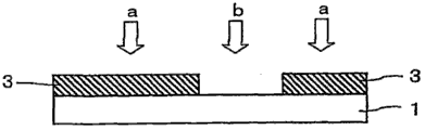
Among the figure, 1-film substrate, 2-undercoat, 3-transparent conductor layer, 4-adhesive phase, 5-transparent base, 6-hard conating, a-drafting department, the non-drafting department of b-.
Embodiment
Following with reference to figure explanation embodiments of the present invention.Fig. 1 is the sectional view of an example of expression transparent conducting film of the present invention.The transparent conducting film of Fig. 1 has transparent conductor layer 3 at the single face of clear films base material 1 via undercoat 2.Transparent conductor layer 3 is patterned.Wherein, in each figure, transparent conductor layer 3 is patterned the non-drafting department b that is meant the drafting department a with transparent conductor layer 3 and does not have transparent conductor layer 3.In addition, has described undercoat 2 at described non-drafting department b.Fig. 2, the 3rd has the situation of two base coats 2.In Fig. 2,3, set gradually undercoat 21,22 from clear films base material 1 side.Fig. 2 is the situation that has undercoat 21,22 at non-drafting department b.Among Fig. 3, similarly be patterned with transparent conductor layer 3 from clear films base material 1 undercoat 22 farthest.In Fig. 3, has undercoat 21 at non-drafting department b.That is, have under the situation of two base coats 2, begin to have ground floor undercoat 21 at least from clear films base material 1 side at non-drafting department b.In Fig. 2,3, illustration the situation of two base coats 2, but undercoat 2 also can be for more than three layers.Even have under the situation of undercoat more than three layers, also have at least from clear films base material 1 side at non-drafting department b and to begin ground floor undercoat 21.The upside undercoat of ground floor can be patterned or not be patterned.At least have under the situation of two base coats 2, preferably the reflection differences with drafting department a and non-drafting department b is controlled to be less.Particularly under the situation that has two base coats 2 at least, for the reflection differences with drafting department a and non-drafting department b is controlled to be less, preferably from clear films base material undercoat farthest (as Fig. 3, have under the situation of two base coats 2, be undercoat 22) similarly be patterned with transparent conductor layer 3.In addition, Fig. 4 is the situation that does not have the transparent conductor layer 3 that has been patterned at the single face of clear films base material 1 via undercoat 2.
Fig. 5 also represents the sectional view of an example of transparent conducting film of the present invention.Wherein, in Fig. 5, use the structure identical to describe, in Fig. 5, also can be suitable for the structure identical certainly with the structure that in Fig. 2, Fig. 3, has illustrated with Fig. 1.The transparent conducting film of Fig. 5 is the situation that has the transparent conductor layer 3 that has been patterned on the two sides of clear films base material 1 via undercoat 2.Wherein, the transparent conducting film of Fig. 5 has the transparent conductor layer 3 that has been patterned in both sides, but also can only be patterned in a side.In addition, the drafting department a of the transparent conductor layer 3 that the transparent conducting film of Fig. 5 has been patterned in both sides is consistent with non-drafting department b, but they also can be inconsistent, can be with various patterns patterning suitably.Also identical in other figure.
Fig. 6~Fig. 9 also represents the sectional view of an example of transparent conducting film of the present invention.In the transparent conducting film of Fig. 6~Fig. 9, via two described Fig. 1 of transparent adhesives layer 4 lamination or transparent conducting film shown in Figure 5.In addition, in Fig. 6~Fig. 9, the transparent conducting film that lamination obtains is become in the described transparent conductor layer that has been patterned 3 of single face configuration at least by lamination.In Fig. 6~Fig. 7, via two transparent conducting films shown in Figure 1 of transparent adhesives layer 4 lamination.In Fig. 6, be on the clear films base material 1 of transparent conducting film shown in Figure 1, via the situation of the transparent conductor layer that has been patterned 3 of transparent adhesives layer 4 other transparent conducting film of lamination.In Fig. 7, be between the clear films base material 1 of transparent conducting film shown in Figure 1 via the situation of transparent adhesives layer 4 lamination.Among Fig. 8~Fig. 9, via transparent adhesives layer 4 lamination transparent conducting film shown in Figure 1 and transparent conducting film shown in Figure 5.In Fig. 8, be the situation of the transparent conductor layer 3 that has been patterned of the single face of the transparent conductor layer that has been patterned 3 and the transparent conducting film shown in Figure 5 of transparent conducting film shown in Figure 1 via transparent adhesives layer 4 lamination.In Fig. 9, be the situation of the transparent conductor layer 3 that has been patterned of the single face of clear films base material 1 and the transparent conducting film shown in Figure 5 of transparent conducting film shown in Figure 1 via transparent adhesives layer 4 lamination.In Fig. 6~Fig. 9, illustration Fig. 1 or transparent conducting film shown in Figure 5 situation via two transparent adhesives layer 4 laminations, but Fig. 1 or transparent conducting film shown in Figure 5 also can suitably make up more than 3 according to the pattern of above-mentioned Fig. 6~Fig. 9.Wherein, among Fig. 6~Fig. 9, use the structure identical to describe, but in Fig. 6~Fig. 9 with Fig. 1, can certainly be suitable for in Fig. 2, structure that structure illustrated in fig. 3 is identical.
In addition, transparent conducting film of the present invention can use with the pattern that adhesive phase 4 is set.Adhesive phase 4 is the described transparent conductor layer that has been patterned 3 of single face configuration at transparent conducting film by lamination.Figure 10 is the situation at the clear films base material 1 superimposed layer transparent adhesives layer 4 of transparent conducting film shown in Figure 1.Figure 11 is the situation of the transparent conductor layer 3 superimposed layer transparent adhesives layers 4 that have been patterned of the single face at transparent conducting film shown in Figure 5.In Figure 10, Figure 11, separator S is set on adhesive phase 4.In addition, for for the situation of two above transparent conducting films of lamination of Fig. 6~shown in Figure 9, also can be similarly with in the mode of the described transparent conductor layer that has been patterned 3 of single face configuration of transparent conducting film and stack adhesive layer 4.
In addition, can be at the single face of described transparent conducting film via transparent adhesives layer 4 applying transparent base 5.The transparent conducting film that is fitted with transparent base 5 is with in the mode of the described transparent conductor layer that has been patterned 3 of single face configuration and applying transparent base 5.Figure 12 is that clear films base material 1 (single face of transparent conductor layer 3 is not set) at the transparent conducting film of Fig. 1 is via the transparent conducting film of the structure of transparent adhesives layer 4 applying transparent base 5.Transparent base 5 can be made of 1 matrix film, also can be the laminated body (via the laminated body of transparent adhesives lamination layer) of the matrix film more than two.In addition, Figure 12 is the situation that hard conating (resin bed) 6 is set at the outside surface of transparent base 5.In Figure 12, illustration the transparent conducting film of Fig. 1, but identical structure also can be suitable for Fig. 2,3 transparent conducting film.In addition, also can be suitable for the transparent conducting film of the structure of Fig. 5~Fig. 9 etc.
As described film substrate 1, be not particularly limited, can use various plastic sheetings via the transparency.For example, as its material, can enumerate polyester based resin, acetate and be resin, polyethersulfone and be resin, polycarbonate-based resin, polyamide-based resin, polyimide and be resin, polyolefin-based resins, (methyl) acrylic resin, polyvinyl chloride resin, polyvinylidene chloride resin, polystyrene resin, polyvinyl alcohol resin, poly-arylation system resin, polyphenylene sulfide is resin etc.Wherein, special preferred polyester is resin, polycarbonate-based resin, polyolefin-based resins.
In addition, open in the 2001-343529 communique (WO 01/37007) macromolecule membrane of record the spy, can be exemplified as comprise (A) side chain have replace and/or not substituted imido thermoplastic resin and (B) have the resin combination of the thermoplastic resin of replacement and/or unsubstituted phenyl and itrile group at side chain.As concrete example, can be exemplified as and contain by the contract macromolecule membrane of resin combination of alternating copolymer that imines forms and acrylonitrile styrene copolymer of isobutylene and N-methyl maleic anhydride.
The thickness of described film substrate 1 is preferably in the scope of 2~200 μ m, more preferably in the scope of 2~100 μ m.If the thickness of film substrate 1 is less than 2 μ m, then the physical strength of film substrate 1 is not enough, is difficult to sometimes make this film substrate 1 become the roller shape and the operation that forms undercoat 2, transparent conductor layer 3 continuously.On the other hand, if thickness surpasses 200 μ m, then can not realize the mar resistance of transparent conductor layer 3 or the raising of using as touch panel of getting characteristic ready sometimes.
Also can implement etch processes or primary coat processing such as sputter, corona discharge, flame, ultraviolet ray irradiation, electron ray irradiation, chemical produced film, oxidation in advance, thereby improve the adhesiveness that the described relatively film substrate 1 of undercoat 2 thereon is set to the surface of described film substrate 1.In addition, before undercoat 2 is set, also can utilize dedusting, cleaningizations such as solvent cleaning or ultrasonic cleaning as required.
In the present invention, even under the situation of patterning transparent conductor layer 3,, also can obtain the good display element of outward appearance by having undercoat 2.From then on viewpoint is set out, and the difference of the refractive index of the refractive index preferably clear conductor layer 3 of undercoat 2 and the refractive index of undercoat has more than 0.1.The difference of the refractive index of transparent conductor layer 3 and the refractive index of undercoat is preferably more than 0.1 below 0.9, and then is preferably more than 0.1 below 0.6.In addition, the refractive index of undercoat 2 is generally 1.3~2.5, and then is preferably 1.38~2.3, and then more preferably 1.4~2.3
In addition, as organism, can enumerate acryl resin, urethane resin, melamine resin, alkyd resin, siloxane-based polymers, organosilane condensation product etc.These organism can use at least a.As organism, the preferred especially thermohardening type resin that uses the potpourri by melamine resin and alkyd resin and organosilane condensation product to constitute.
Form by organism from the undercoat of the ground floor of clear films base material 1 beginning, preferably utilize etched pattern transparent conductor layer 3.Thereby undercoat 2 is under the situation of one deck, and undercoat 2 is preferably formed by organism.
In addition, have at least under the situation of two base coats 2,, preferably form by inorganics from clear films base material 1 undercoat farthest at least from utilizing the angle of etched pattern transparent conductor layer 3.Have under the situation of undercoat 2 more than 3 layers,, preferably form by inorganics for for the undercoat more than the clear films base material 1 beginning second layer.
The undercoat that is formed by inorganics can utilize dry type processes such as vacuum vapour deposition, sputtering method, ion plating method or wet method (coating process) etc. to form.As the inorganics that forms undercoat, as mentioned above, preferred SiO
2In the wet method, can be by formation SiO such as coating silica sols
2Film.
From as can be known above, be provided with under the situation of two base coats 2, first undercoat 21 that preferably utilizes organism to form utilizes inorganics to form second undercoat 22.
Thickness to undercoat 2 is not particularly limited, and from optical design, prevent to take place from described film substrate 1 to be generally the point of the effect of oligomer about 1~300nm, is preferably 5~300nm.In addition, be provided with under the situation of two-layer above undercoat, the thickness of each layer is about 5~250nm, is preferably 10~250nm.
As mentioned above, transparent conductor layer 3 is preferably more than 0.1 with the difference of the refractive index of undercoat 2.The refractive index of transparent conductor layer 3 is generally about 1.95~2.05.
Constituent material as described transparent conductor layer 3 is not particularly limited, and can use the metal oxide of at least a metal of selecting from the group that indium, tin, zinc, gallium, antimony, titanium, silicon, zirconium, magnesium, aluminium, gold, silver, copper, palladium, tungsten constitute.As required, also can and then contain the metallic atom shown in above-mentioned group in this metal oxide.For example can preferably use the indium oxide that contains tin oxide, the tin oxide that contains antimony etc.
Thickness to transparent conductor layer 3 is not particularly limited, and is 1 * 10 in order to become its surface resistance
3The continuous tunicle with good electrical conductivity that Ω/ is following, preferred thickness is more than the 10nm.If it is blocked up that thickness becomes, then can cause the reduction of the transparency etc., thus preferred 15~35nm, more preferably in the scope of 20~30nm.Thickness is during less than 15nm, and it is too high that surface resistance becomes, and be difficult to become continuous tunicle.In addition, if surpass 35nm, then can cause the reduction of the transparency etc.
Formation method as transparent conductor layer 3 is not particularly limited, and can adopt known method in the past.Particularly, for example can the illustration vacuum vapour deposition, sputtering method, ion plating method.In addition, as required, also can adopt suitable method by corresponding thickness.In addition, after forming transparent conductor layer 3, as required, can in 100~150 ℃ scope, implement annealing in process, make its crystallization.So film substrate 1 preferably has more than 100 ℃ and then the thermotolerance more than 150 ℃.In the present invention, transparent conductor layer 3 etched patternings.If crystallization transparent conductor layer 3 then is difficult to etching sometimes, so the annealing processing of transparent conductor layer 3 is preferably carried out after patterning transparent conductor layer 3.And then, under the situation of etching undercoat 2, after etching undercoat 2, preferably carry out the annealing processing of transparent conductor layer 3.
The manufacture method of transparent conducting film of the present invention is so long as on the single face or two sides of clear films base material, and undercoat and transparent conductor layer have said structure and get final product, and its manufacture method is not particularly limited.For example, can be according to routine, be formulated in the single face of clear films base material or two sides and begin the transparent conducting film that has transparent conductor layer via 1 layer of undercoat at least, thereby make by the described transparent conductor layer patterning of etching then from a side of film substrate.During etching, the mask that is used to form pattern covers transparent conductor layer, utilizes etching solution, the etching transparent conductor layer.
Transparent conductor layer can preferably be used the indium oxide that contains tin oxide, the tin oxide that contains antimony, so as etching solution, can preferably use acid.As acid, for example can enumerate mineral acids such as hydrogen chloride, hydrogen bromide, sulfuric acid, nitric acid, phosphoric acid, organism and their potpourri and their aqueous solution such as acetic acid.
At least have under the situation of two base coats, only etching transparent conductor layer is come patterning, in addition, thereby also can be after utilizing acid etching transparent conductor layer patterning, thus with transparent conductor layer similarly at least etching from clear films base material undercoat patterning farthest.Thereby preferably can with the transparent conductor layer patterning of transparent conductor layer etching similarly except the undercoat that begins ground floor from the clear films base material.
When the etching undercoat, the mask that is used to form with the same pattern of the situation of etching transparent conductor layer covers undercoat, utilizes etching solution, the etching undercoat.As mentioned above, the undercoat on the second layer preferably uses SiO
2Deng inorganics, so, can preferably use alkali as etching solution.As alkali, for example can enumerate the aqueous solution of NaOH, potassium hydroxide, ammoniacal liquor, tetramethylammonium hydroxide etc. and their potpourri.In addition, the transparent conductor layer of ground floor is preferably by not formed by the organism of acid or alkaline etching.
In transparent conducting film of the present invention, be patterned via the two base coats setting the situation of transparent conductor layer under, from the difference of the reflectivity of drafting department and non-drafting department being designed to less point, preferably (sum total of n * d) is as described below for the optical thickness of described each layer of the refractive index (n) of each layer in this drafting department, thickness (d).
The refractive index (n) of the undercoat that begins from the ground floor of clear films base material is preferably 1.5~1.7, and then is preferably 1.5~1.65, and then more preferably 1.5~1.6.Thickness (d) is preferably 100~220nm, and then is preferably 120~215nm, and then 130~210nm more preferably.
The refractive index (n) that begins the undercoat of the second layer from the clear films base material is preferably 1.4~1.5, and then is preferably 1.41~1.49, and then more preferably 1.42~1.48.Thickness (d) is preferably 20~80nm, and then is preferably 20~70nm, and then 20~60nm more preferably.
The refractive index of transparent conductor layer (n) is preferably 1.9~2.1, and then is preferably 1.9~2.05, and then more preferably 1.9~2.0.Thickness (d) is preferably 15~30nm, and then is preferably 15~28nm, and then 15~25nm more preferably.
(sum total of n * d) is preferably 208~554nm to the optical thickness of described each layer (undercoat of ground floor, the undercoat of the second layer, transparent conductor layer), and then is preferably 230~500nm, and then 250~450nm more preferably.
In addition, poor (the Δ nd) of the optical thickness of the undercoat of the sum total of the optical thickness of described drafting department and non-drafting department is preferably 40~130nm.Poor (the Δ nd) of described optical thickness and then be preferably 40~120nm, and then 40~110nm more preferably.
As mentioned above, transparent conducting film of the present invention can be via at least two of transparent adhesives layer 4 laminations in the mode in the described transparent conductor layer that has been patterned 3 of the configuration of single face at least.In addition, transparent conducting film of the present invention can lamination transparent adhesives layer 4 in the mode in the described transparent conductor layer that has been patterned 3 of single face configuration.
In addition, the mode of the transparent conductor layer 3 that has been patterned with the single face configuration of the transparent conducting film that is fitted with transparent base 5 can be at the single face of transparent conducting film of the present invention via transparent adhesives layer 4 applying transparent base 5.Transparent base 5 also can be bonded to the composite structure of few two transparent matrix films for utilizing the transparent adhesives laminating.In addition, the patterning of described transparent conductor layer 3 also can become the transparent conducting film enforcement of this structure relatively.
The thickness of transparent base 5 preferably is controlled as 90~300 μ m usually, more preferably 100~250 μ m.In addition, under the situation about forming by a plurality of matrix films that form transparent base 5, the thickness of each matrix film is preferably 10~200 μ m, and then be preferably 20~150 μ m, be controlled in the described scope as the gross thickness of the transparent base 5 that comprises these matrix films and transparent adhesives layer.As the matrix film, can enumerate and above-mentioned film substrate 1 identical materials.
Transparent conducting film (for example film substrate 1) also can be provided with described adhesive phase 4 for the side at transparent base 5 with the applying of transparent base 5, to its described film substrate 1 of fitting, also can be opposite, in film substrate 1 side described adhesive phase 4 is set, to its applying transparent base 5.In the latter's method, the formation of adhesive phase 4 can make film substrate 1 become the roller shape and carry out continuously, so from the aspect of throughput rate, more favourable.In addition, also can on film substrate 1, utilize adhesive phase a plurality of matrix films of fitting to come lamination transparent base 5 successively.Wherein, the transparent adhesives layer that uses in the lamination of matrix film can use and following transparent adhesives layer 4 identical materials.In addition, in the time of between the applying transparent conducting film, can suitably select the face of the lamination transparent conducting film of stack adhesive layer 4, fit between the transparent conducting film.
As adhesive phase 4, can use so long as have the adhesive phase of the transparency, be not particularly limited.Particularly, for example can suitably select to use with material such as the polymkeric substance of rubber systems such as acrylic acid series polymeric compounds, silicone-based polymkeric substance, polyester, polyurethane, polyamide, polyvinylether, vinyl acetate/vinyl chloride copolymer, improved polyalkene, epoxy system, fluorine system, natural rubber, synthetic rubber etc. as base polymer.From at the adhesion characteristic of outstanding aspect the optical transparence, as to show appropriateness wetting state and coherency and cementability, in the outstanding angle in aspects such as against weather or thermotolerance, preferably use acrylic adhesive.
Kind difference according to as the bonding agent of the constituent material of adhesive phase 4 can improve the throwing anchor-hold by using the suitable bonding silane coupling agent of using.Thereby, use under the situation of such bonding agent, preferably use the bonding silane coupling agent of using.
As the described bonding silane coupling agent of using, get final product so long as can improve the layer of the throwing anchor-hold of bonding agent, be not particularly limited.Particularly, for example can use and in a part, have amino, vinyl, epoxy radicals, sulfydryl, the silane series coupling agent of chloro isoreactivity functional group and water-disintegrable alkoxysilyl, the titanate esters that has the water-disintegrable water wettability base of titaniferous and organic functional base in a part is coupling agent and has the water-disintegrable water wettability base that contains aluminium and the aluminic acid ester of organo-functional group base is so-called coupling agents such as coupling agent in a part that epoxy is a resin, the isocyanate-based resin, polyurethane series resin, ester polyurethane is the resin that resin etc. has the organic reaction base.From industrial maneuverable viewpoint, especially preferably contain the layer of silane series coupling agent.
In addition, in described adhesive phase 4, can contain the crosslinking chemical corresponding with base polymer.In addition in adhesive phase 4, proper additive such as the filling agent that can contain for example natural or synthetic resin as required, constitute by glass fibre, beaded glass, metal powder or other inorganic powder etc., pigment, colorant, antioxidant.Also can be to contain transparent particulate and the diffusible adhesive phase 4 of display light in addition.
In addition, described transparent particulate can use more than a kind or 2 kinds mean grain size for example be 0.5~20 μ m by electric conductivity such as silicon dioxide, calcium oxide, aluminium oxide, titanium dioxide, zirconia, tin oxide, indium oxide, cadmium oxide, antimony oxide inorganic be particulate, the crosslinked or uncrosslinked suitable transparent particulates such as organic system particulate that constitute by the suitable polymkeric substance of polymethylmethacrylate, polyurethane and so on.
Described adhesive phase 4 is usually as being that binder solution about 10~50 weight % uses with base polymer or its composition dissolves or the solid component concentration that is scattered in the solvent gained.As described solvent, kind that can corresponding bonding agent suitably selects to use organic solvents such as toluene or ethyl acetate or water etc.
This adhesive phase 4 has function as described below, that is: for example after bonding transparent base 5, utilize its buffering effect, improve the single face be arranged at film substrate 1 transparent conductor layer mar resistance or get characteristic, so-called pen input permanance and surface pressing permanance ready as what touch panel was used.From bringing into play this functional point of view better, the elastic modulus that preferably makes adhesive phase 4 is at 1~100N/cm
2Scope, thickness be the above scope of 1 μ m, preferably set scope usually at 5~100 μ m.If be described thickness, then can bring into play above-mentioned effect fully, transparent base 5 is also abundant with the adhesion of film substrate 1.If thinner than above-mentioned scope, then can not guarantee above-mentioned permanance or adhesiveness fully, in addition,, then may produce bad situation in outward appearances such as the transparencys if thicker than above-mentioned scope.In addition, the elastic modulus of the adhesive phase 4 of transparent conducting film Zhang Shiyong, thickness are also same as described above in other patterns.
If described elastic modulus is less than 1N/cm
2, then adhesive phase 4 become non-resilient, so when pressurization easy deformation, produce concavo-convex at film substrate 1 and then transparent conductor layer 3.In addition, easily from processing section extrusioning adhesive etc., and lower the mar resistance of transparent conductor layer 3 or the raising effect of using as touch panel of getting characteristic ready.On the other hand, if elastic modulus surpasses 100N/cm
2, then adhesive phase 4 hardening can not realize its buffering effect, so there is the trend that is difficult to improve the mar resistance of transparent conductor layer 3 or imports permanance and surface pressing permanance as the pen that touch panel is used.
In addition, if the thickness of adhesive phase 4 then can not be realized its buffering effect less than 1 μ m, so there is the trend that is difficult to improve the mar resistance of transparent conductor layer 3 or imports permanance and surface pressing permanance as the pen that touch panel is used.On the other hand, if blocked up, then can damage the transparency, the applying operability of the formation of adhesive phase 4 or transparent base 5 and then cost aspect all are difficult to pay off.
The transparent base 5 of fitting via adhesive phase 4 like this is except film substrate 1 being given excellent mechanical intensity, pen input permanance and surface pressing permanance, the member of the generation that especially helping prevents to curl waits.
Using under the situation of described separator S transfer printing adhesive phase 4, as such separator S, for example preferred the use moved the mylar that prevents layer and/or release layer etc. with the bonding face lamination of adhesive phase 4 at least at mylar.
The gross thickness of described separator S is preferably more than the 30 μ m, more preferably in the scope of 60~100 μ m.Form after the adhesive phase 4, under the situation with the keeping of roller state, can suppress owing to enter the distortion (beating trace) of the possible adhesive phase 4 of the generations such as foreign matter between roller.
Prevent layer as described move, can form by the suitable material that moves of the low-molecular weight oligo thing composition of the mobile composition, the particularly polyester that are used for preventing mylar.As moving the formation material that prevents layer, can use inorganics or organism or their compound substance.Can suitably set with the scope of 0.01~20 μ m and move the thickness that prevents layer.As moving the formation method that prevents layer, be not particularly limited, for example can use coating process, gunite, spin-coating method, streamline coating process etc.In addition, also can use vacuum vapour deposition, sputtering method, ion plating method, injection thermal decomposition method, electroless plating method, electrochemical plating etc.
As described release layer, can form the layer that constitutes by suitable release agents such as silicone-based, chain alkyl system, fluorine system, molybdenum sulfides.Can suitably set the thickness of release layer from the point of stripping result.Usually from the point of operability such as flexibility, this thickness is preferably below the 20 μ m, more preferably in the scope of 0.01~10 μ m, is preferably especially in the scope of 0.1~5 μ m.Formation method as release layer is not particularly limited, and can adopt and the described identical method of formation method that prevents layer that moves.
In described coating process, gunite, spin-coating method, streamline coating process, can use acrylic resin, polyurethane series resin, melamine be resin, epoxy be ionizing radiation curing type resins such as resin or in described resin the material of mixed aluminium oxides, silicon dioxide, mica etc.In addition, use under the situation of vacuum vapour deposition, sputtering method, ion plating method, injection thermal decomposition method, electroless plating method or electrochemical plating, can use by gold, silver, platinum, palladium, copper, aluminium, nickel, chromium, titanium, iron, cobalt or be or other metallic compounds that metal oxide that their alloy etc. constitutes, cupric iodide etc. constitute.
In addition, as required, can be that purpose is provided with hard conating (resin bed) 6 with the protection outside surface also at the outside surface (with the face of adhesive phase 4 opposition sides) of described transparent base 5.As hard conating 6, for example can preferably use melamine is that resin, polyurethane series resin, alkyd are the curing tunicle that gel-type resins such as resin, acrylic resin, silicone-based resin constitute.As the thickness of hard conating 6, be preferably 0.1~30 μ m.If thickness is less than 0.1 μ m, then hardness is not enough sometimes.In addition, if the crack, then may take place above 30 μ m in thickness in hard conating 6 or whole transparent base 5 takes place to curl.
In addition, also can in transparent conducting film of the present invention, be provided for improving the non-glare treated layer or the anti-reflection layer of identification.Under the situation about in the touch panel of resistive film mode, using, can similarly non-glare treated layer or anti-reflection layer be set with described hard conating 6 at the outside surface (with the face of adhesive phase 4 opposition sides) of described transparent base 5.In addition, also can on described hard conating 6, non-glare treated layer or anti-reflection layer be set.On the other hand, under the situation about using in the touch panel of electrostatic capacitance mode, non-glare treated layer or anti-reflection layer also can be arranged on the transparent conductor layer 3.
Constituent material as the non-glare treated layer is not particularly limited, and for example can use ionizing radiation curing type resin, thermohardening type resin, thermoplastic resin etc.The thickness of non-glare treated layer is preferably 0.1~30 μ m.
As anti-reflection layer, can use titanium dioxide, zirconia, monox, magnesium fluoride etc.In order to show anti-reflective function biglyyer, preferably use the laminated body of titanium oxide layer and silicon oxide layer.About 1.8), form the lower silicon oxide layer of refractive index (refractive index: two-layer laminated body about 1.45), and then be preferably the 4 layer laminate bodies that form titanium oxide layer and silicon oxide layer on this two-layer laminated body successively on this titanium oxide layer described laminated body is preferably and is forming the higher titanium oxide layer of refractive index (refractive index: on the hard conating 6.By the so two-layer laminated body or the anti-reflection layer of 4 layer laminate bodies are set, can lower wavelength region may (380~780nm) the reflection of luminous ray equably.
Transparent conducting film of the present invention for example preferably is applicable to touch panels such as optical mode, ultrasound wave mode, electrostatic capacitance mode, resistive film mode.Be particularly preferred for the touch panel of electrostatic capacitance mode.In addition, transparent conducting film of the present invention for example can be applicable to that electrophoresis flowing mode, distortion ball (twist ball) mode, thermogravimetric write (thermal rewritable) mode, light and read in liquid crystal mode, polymer dispersion type liquid crystal mode, guest-master (guest-host) liquid crystal mode, toner display mode, parachroia (chromism) mode, electric field and separate out flexible display elements such as mode.
Embodiment
Below explain the present invention with embodiment, but the present invention is not limited by following examples in the scope that does not exceed its main idea.In addition, in each example, part, % are weight standard.
<refractive index 〉
The refractive index of each layer is used the Abbe refractomecer of ア タ go corporate system, makes mensuration light incide various mensuration faces, utilizes the assay method of the regulation shown in this refractometer to measure.
The thickness of<each layer 〉
Film substrate, transparent base, hard conating, adhesive phase etc. are had the layer of the above thickness of 1 μ m, utilize ミ Star ト ヨ system precise ultrasonic thicknessmeter (MICROGAGE) formula thickness meter to measure.Under the situation of layer that is very difficult direct instrumentation thickness such as hard conating, adhesive phase, lamination is provided with the gross thickness of the base material of each layer, calculates the thickness of each layer by the thickness that deducts base material.
The thickness of the undercoat of ground floor, the undercoat of the second layer, ITO film etc. uses big
 The MCPD2000 (trade name) as moment multi photometry system of electronics (strain) system is that calculate on the basis with the waveform that utilizes interference spectrum.
The surface resistance of<undercoat 〉
According to the two-coil method (double リ Application グ method) that with JIS K 6911 (1995) is standard, use the surperficial high resistance meter of Mitsubishi Chemical's (strain) system, the surface resistance of mensuration undercoat (Ω/).
(embodiment 1)
(formation of undercoat)
At thickness is the single face of the film substrate that constitutes of the pet film (hereinafter referred to as the PET film) of 25 μ m, utilize melamine resin: alkyd resin: 2: 2: 1 thermohardening type resin of the weight ratio of organosilane condensation product (refractive index n of light=1.54), forming thickness is the ground floor undercoat of 185nm.Then, (コ Le コ one ト (strain) makes with silica sol with ethanol, コ Le コ one ト P) is diluted to solid component concentration 2%, on the undercoat of ground floor, utilize the coating of monox coating process, then, drying is 2 minutes under 150 ℃, it is solidified, and forming thickness is the second layer undercoat (SiO of 33nm
2Film, the refractive index 1.46 of light).The undercoat surface resistance afterwards that forms ground floor, the second layer is 1 * 10
12More than Ω/.
(formation of transparent conductor layer)
Then, on the undercoat of the second layer, in the atmosphere of the 0.4Pa that argon gas 98% and oxygen 2% constitute, utilize reactive sputtering method with the sintered material of indium oxide 97 weight %, tin oxide 3 weight %, forming thickness is the ITO film (refractive index 2.00 of light) of 22nm, obtains transparent conducting film.
(formation of hard conating)
Formation material as hard conating, in acroleic acid polyurethane is 100 parts of resins (the ユ ニ デ イ Star Network 17-806 of big Japanese ink (イ Application キ) chemistry (strain) system), adding is as 5 parts of the hydroxy-cyclohexyl phenyl ketones (Irgacure184 of the special chemical drug company system of Chiba) of Photoepolymerizationinitiater initiater, the toluene solution that prepared and diluted becomes the concentration of 30 weight % to form.
At thickness is the single face of the transparent base that constitutes of the PET film of 125 μ m, applies the formation material of this hard conating, 100 ℃ dry 3 minutes down.Then, immediately with ozone type high-pressure sodium lamp (energy density 80W/cm
2, the 15cm light-focusing type) and irradiation ultraviolet radiation under 2 lamps, forming thickness is the hard conating of 5 μ m.
(making of lamination transparent conducting film)
Then, forming the face of the opposition side of face, forming that thickness is about 20 μ m, elastic modulus is 10N/cm with the hard conating of described transparent base
2Transparent acrylic adhesive layer.As the adhesive phase composition, using weight ratio at butyl acrylate and acrylic acid and vinyl acetate is to cooperate 1 part of composition that the isocyanate-based crosslinking chemical forms in 100: 2: 5 100 parts of the acrylic acid series copolymers.At the described adhesive phase side above-mentioned transparent conducting film (not forming the face of a side of transparent conductor layer) of fitting, make the lamination transparent conducting film.
(ITO film pass through etched patterning)
Coating, dry solidification have been patterned to the photoresist of striated on the transparent conductor layer of lamination transparent conducting film, flood 1 minute in 25 ℃, 5% hydrochloric acid (hydrochloride aqueous solution) then, carry out the etching of ITO film.
(undercoat of the second layer pass through etched patterning)
After the etching of carrying out above-mentioned ITO film, then under the state of lamination photoresist, dipping is 3 minutes in 45 ℃, 2% sodium hydrate aqueous solution, carries out the etching of the undercoat of the second layer, removes photoresist then.
(crystallization of transparent conductor layer)
After the etching of the undercoat of the described second layer, under 140 ℃, carry out 90 minutes heat treated, crystallization ITP film.
In embodiment 1, do not carry out the second layer undercoat pass through etched patterning, in addition, carry out same operation with embodiment 1, make the lamination transparent conducting film of patterning ITO film.
In embodiment 1, the thickness of the undercoat of ground floor is become 35nm, do not form the undercoat of the second layer, in addition, carry out same operation with embodiment 1, make the lamination transparent conducting film of patterning ITO film.
In embodiment 1, the thickness of the undercoat of ground floor is become 150nm, in addition, carry out same operation with embodiment 1, make the lamination transparent conducting film of patterning ITO film.
In embodiment 1, the thickness of the undercoat of ground floor is become 150nm, do not carry out the second layer undercoat pass through etched patterning, in addition, carry out same operation with embodiment 1, make the lamination transparent conducting film of patterning ITO film.
In embodiment 2~5, the undercoat surface resistance afterwards that forms ground floor, the second layer is 1 * 10
12More than Ω/.
Comparative example 1
In embodiment 1, do not form the undercoat of ground floor, the undercoat of the second layer, in addition, carry out same operation with embodiment 1, make the lamination transparent conducting film of patterning ITO film.
Comparative example 2
In embodiment 1, replace the undercoat of ground floor and the ITO film that thickness is 33nm is set, the thickness of the undercoat of the second layer is become 60nm, do not carry out the second layer undercoat pass through etched patterning, in addition, carry out same operation with embodiment 1, make the lamination transparent conducting film of patterning ITO film (transparent conductor layer on surface).Undercoat (ITO film) surface resistance afterwards that forms ground floor is 2 * 10
2Ω/, the undercoat surface resistance afterwards that forms the second layer is 4 * 10
2Ω/.
Lamination transparent conducting film (sample) in embodiment and comparative example carries out following evaluation.The result is shown in table 1, table 2.
The sheet resistance value of<ITO film 〉
Resistance value between the pattern of<ITO film 〉
To the drafting department of self-existent ITO film, utilize tester (tester), measure resistance (Ω), whether evaluation is insulated.As long as 1 * 10
6More than the Ω, just can be judged as insulation.Tester uses the digital tester (digital tester) " CDM-2000D " of カ ス タ system corporate system.
The transmitance of<light 〉
Use the spectroscopy apparatus UV-240 of Shimadzu Seisakusho Ltd.'s system, measure the luminous ray transmitance under the optical wavelength 550nm.
The Y value of the average reflectance of<450~650nm, reflection 〉
Use the integrating sphere mode determination of the spectrophotometer U4100 of (strain) Hitachi system, making and being reflected into firing angle is 10 degree, measures reflectance spectrum, calculates the average reflectance and the Y value in 450~650nm zone.Wherein, described mensuration uses the black sprayer to form light shield layer in the rear side (hard conating side) of lamination transparent conducting film (sample), measures under backside reflection that does not almost have sample or the state from the incident of the light of rear side.The light D of specified standard among the JIS Z8720 is adopted in the calculating of reflection color
65, under the condition in the 2 degree visuals field, measure.Drafting department (ITO film) and non-drafting department (etched part) average the mensuration of reflectivity and Y value respectively.In addition, drafting department is shown in table 2 with poor (the Δ reflectivity) of the reflectivity of non-drafting department, poor (the Δ Y value) of Y value.
<ocular estimate 〉
On the plate of ?, place sample, make above its transparent conductor layer becomes, utilize visually, whether can distinguish drafting department and non-drafting department with following standard evaluation.
◎: be difficult to distinguish drafting department and non-drafting department.
Zero: can distinguish drafting department and non-drafting department slightly.
*: can clearly distinguish drafting department and non-drafting department.
[table 1]

In the table 1, AC (layer) represents hard conating.
[table 2]

From table 1, table 2 as can be known, the transparent conductor layer of transparent conducting film of the present invention is patterned, and outward appearance is good.
Claims (15)
1. the manufacture method of a transparent conducting film, wherein transparent conducting film is on the single face or two sides of clear films base material, has transparent conductor layer via one deck undercoat ground at least, and described transparent conductor layer is patterned, and the transparent conducting film that has the described undercoat of one deck at least at the non-drafting department that does not have described transparent conductor layer, the manufacture method of described transparent conducting film is characterised in that
On the single face or two sides of clear films base material, utilize organism to form the operation that begins the undercoat of ground floor from the clear films base material;
On described undercoat, utilize sputtering method to form the operation of transparent conductor layer; And
Operation with described transparent conductor layer etching and patterning.
2. the manufacture method of transparent conducting film according to claim 1 is characterized in that,
The organism that forms undercoat contains select at least a from the group that acryl resin, urethane resin, melamine resin, alkyd resin, siloxane-based polymers, organosilane condensation product constitute.
3. the manufacture method of transparent conducting film according to claim 1 is characterized in that,
Undercoat has two-layer at least, is formed by inorganics from clear films base material undercoat farthest at least.
4. the manufacture method of transparent conducting film according to claim 3 is characterized in that,
The SiO of the undercoat that forms by inorganics for forming by the coating silica sol
2Film.
5. the manufacture method of transparent conducting film according to claim 1 is characterized in that,
The difference of the refractive index of transparent conductor layer and the refractive index of undercoat is more than 0.1.
6. transparent conducting film, it is on the single face or two sides of clear films base material, has transparent conductor layer via one deck undercoat ground at least, and described transparent conductor layer is patterned, and the transparent conducting film that has the described undercoat of one deck at least at the non-drafting department that does not have described transparent conductor layer, described transparent conducting film is characterised in that
On the single face or two sides of clear films base material, utilize organism to be formed with the undercoat that begins ground floor from the clear films base material;
Described transparent conductor layer utilizes sputtering method to form.
7. transparent conducting film according to claim 6 is characterized in that,
The organism that forms undercoat contains select at least a from the group that acryl resin, urethane resin, melamine resin, alkyd resin, siloxane-based polymers, organosilane condensation product constitute.
8. transparent conducting film according to claim 6 is characterized in that,
Undercoat has two-layer at least, is formed by inorganics from clear films base material undercoat farthest at least.
9. transparent conducting film according to claim 8 is characterized in that,
The SiO of the undercoat that forms by inorganics for forming by the coating silica sol
2Film.
10. transparent conducting film according to claim 6 is characterized in that,
The difference of the refractive index of transparent conductor layer and the refractive index of undercoat is more than 0.1.
11. a transparent conducting film is characterized in that,
The mode of the described transparent conductor layer that has been patterned with configuration on single face at least, via the transparent adhesives layer, two described transparent conducting films of claim 6 of lamination at least.
12. a transparent conducting film is characterized in that,
On single face, to dispose the mode of the described transparent conductor layer that has been patterned, on the single face of the described transparent conducting film of claim 6, via the transparent adhesives layer, the applying transparent base.
13. transparent conducting film according to claim 6 is characterized in that,
Be used to touch panel.
14. transparent conducting film according to claim 13 is characterized in that,
Touch panel is the touch panel of electrostatic capacitance combination.
15. a touch panel is characterized in that,
Possesses each described transparent conducting film in the claim 6~14.
Applications Claiming Priority (4)
| Application Number | Priority Date | Filing Date | Title |
|---|---|---|---|
| JP2007009295 | 2007-01-18 | ||
| JP2007-009295 | 2007-01-18 | ||
| JP2007224232 | 2007-08-30 | ||
| JP2007-224232 | 2007-08-30 |
Related Parent Applications (1)
| Application Number | Title | Priority Date | Filing Date |
|---|---|---|---|
| CN2008100040677A Division CN101226450B (en) | 2007-01-18 | 2008-01-18 | Transparent conductive film, method for production thereof and touch panel therewith |
Publications (1)
| Publication Number | Publication Date |
|---|---|
| CN102184065A true CN102184065A (en) | 2011-09-14 |
Family
ID=39274619
Family Applications (5)
| Application Number | Title | Priority Date | Filing Date |
|---|---|---|---|
| CN2011100430792A Active CN102184754B (en) | 2007-01-18 | 2008-01-18 | Transparent conductive film and touch panel therewith |
| CN2008100040677A Active CN101226450B (en) | 2007-01-18 | 2008-01-18 | Transparent conductive film, method for production thereof and touch panel therewith |
| CN2011100430773A Pending CN102097159A (en) | 2007-01-18 | 2008-01-18 | Transparent conductive film , method for production thereof and touch panel therewith |
| CN2011100430805A Pending CN102097160A (en) | 2007-01-18 | 2008-01-18 | Method for producing transparent conductive film |
| CN2011100430788A Pending CN102184065A (en) | 2007-01-18 | 2008-01-18 | Transparent conductive film, method for fabricating the same and touch panel with it |
Family Applications Before (4)
| Application Number | Title | Priority Date | Filing Date |
|---|---|---|---|
| CN2011100430792A Active CN102184754B (en) | 2007-01-18 | 2008-01-18 | Transparent conductive film and touch panel therewith |
| CN2008100040677A Active CN101226450B (en) | 2007-01-18 | 2008-01-18 | Transparent conductive film, method for production thereof and touch panel therewith |
| CN2011100430773A Pending CN102097159A (en) | 2007-01-18 | 2008-01-18 | Transparent conductive film , method for production thereof and touch panel therewith |
| CN2011100430805A Pending CN102097160A (en) | 2007-01-18 | 2008-01-18 | Method for producing transparent conductive film |
Country Status (6)
| Country | Link |
|---|---|
| US (5) | US8462278B2 (en) |
| EP (5) | EP2312424A2 (en) |
| JP (6) | JP4667471B2 (en) |
| KR (5) | KR101075575B1 (en) |
| CN (5) | CN102184754B (en) |
| TW (5) | TWI449626B (en) |
Families Citing this family (183)
| Publication number | Priority date | Publication date | Assignee | Title |
|---|---|---|---|---|
| TWI289708B (en) | 2002-12-25 | 2007-11-11 | Qualcomm Mems Technologies Inc | Optical interference type color display |
| US7316784B2 (en) * | 2003-02-10 | 2008-01-08 | Lg.Philips Lcd Co., Ltd. | Method of patterning transparent conductive film, thin film transistor substrate using the same and fabricating method thereof |
| US7342705B2 (en) | 2004-02-03 | 2008-03-11 | Idc, Llc | Spatial light modulator with integrated optical compensation structure |
| JP2010510530A (en) | 2006-10-06 | 2010-04-02 | クォルコム・メムズ・テクノロジーズ・インコーポレーテッド | Optical loss structure integrated into lighting equipment |
| EP1943551A2 (en) | 2006-10-06 | 2008-07-16 | Qualcomm Mems Technologies, Inc. | Light guide |
| US8068710B2 (en) | 2007-12-07 | 2011-11-29 | Qualcomm Mems Technologies, Inc. | Decoupled holographic film and diffuser |
| TW200941322A (en) * | 2008-03-28 | 2009-10-01 | Tpk Touch Solutions Inc | Manufacturing method for conducting films on two surfaces of transparent substrate of touch-control circuit |
| WO2010002182A2 (en) | 2008-06-30 | 2010-01-07 | Kolon Industries, Inc. | Plastic substrate and device including the same |
| TWI459436B (en) * | 2008-10-27 | 2014-11-01 | Tpk Touch Solutions Inc | The Method of Making Double - sided Graphic Structure of Touch Circuit |
| KR101219242B1 (en) * | 2009-01-16 | 2013-01-07 | 삼성디스플레이 주식회사 | Touch Screen Panel and Fabricating Method Thereof |
| JP5832065B2 (en) * | 2009-02-05 | 2015-12-16 | 凸版印刷株式会社 | Transparent conductive film |
| JP4775722B2 (en) * | 2009-02-23 | 2011-09-21 | 大日本印刷株式会社 | Touch panel sensor, laminate for manufacturing touch panel sensor, and method for manufacturing touch panel sensor |
| KR100909265B1 (en) * | 2009-02-23 | 2009-07-27 | (주)이엔에이치테크 | Manufacturing method of electrostatic capacity type touch screen panel |
| KR101050460B1 (en) * | 2009-03-25 | 2011-07-20 | 삼성모바일디스플레이주식회사 | OLED display and manufacturing method thereof |
| JP5005112B2 (en) * | 2009-03-31 | 2012-08-22 | 帝人株式会社 | Transparent conductive laminate and transparent touch panel |
| JP4958020B2 (en) * | 2009-03-31 | 2012-06-20 | 大日本印刷株式会社 | Touch panel sensor, laminate for manufacturing touch panel sensor, and method for manufacturing touch panel sensor |
| KR101383673B1 (en) | 2009-04-16 | 2014-04-09 | 박준영 | Pad for preparing touch panel, method of preparing touch panel using the same and touch panel thereby |
| US8599565B2 (en) | 2009-04-21 | 2013-12-03 | Fujitsu Component Limited | Touchscreen panel, electronic apparatus and method of fabricating touchscreen panel |
| JP5401158B2 (en) * | 2009-04-21 | 2014-01-29 | 富士通コンポーネント株式会社 | Touch panel and method for manufacturing touch panel |
| TW201040299A (en) * | 2009-05-05 | 2010-11-16 | Fraunhofer Ges Forschung | Layer system having barrier properties and a structured conductive layer, method for producing the same, and use of such a layer system |
| WO2010143528A1 (en) | 2009-06-11 | 2010-12-16 | 株式会社村田製作所 | Touch screen and touch-type input device |
| WO2010147047A1 (en) * | 2009-06-18 | 2010-12-23 | 日東電工株式会社 | Optical adhesive sheet |
| JP2011016264A (en) * | 2009-07-07 | 2011-01-27 | Innovation & Infinity Global Corp | Structure of transparent conductive film |
| JP5376446B2 (en) * | 2009-07-24 | 2013-12-25 | 株式会社ジャパンディスプレイ | Capacitance type input device and display device with input function |
| TW201108259A (en) | 2009-08-18 | 2011-03-01 | Efun Technology Co Ltd | Film with color homogeneity |
| JP4601710B1 (en) * | 2009-09-11 | 2010-12-22 | 日本写真印刷株式会社 | Narrow frame touch input sheet and manufacturing method thereof |
| EP2477097B1 (en) | 2009-09-11 | 2018-06-06 | Nissha Printing Co., Ltd. | Narrow frame touch input sheet, manufacturing method of same, and conductive sheet used in narrow frame touch input sheet |
| JP5435556B2 (en) * | 2009-09-16 | 2014-03-05 | 日本写真印刷株式会社 | Conductive sheet, laminated conductive sheet and conductive pattern sheet, laminated conductive sheet manufacturing method, transparent antenna or transparent display or touch input sheet manufacturing method |
| JP5259539B2 (en) * | 2009-09-16 | 2013-08-07 | 日本写真印刷株式会社 | Narrow frame touch input sheet with protective film, laminated narrow frame touch input sheet with protective film, and methods for manufacturing the same |
| EP2463759A1 (en) | 2009-09-15 | 2012-06-13 | Sharp Kabushiki Kaisha | Touch panel and display device provided with same |
| JP2011076932A (en) * | 2009-09-30 | 2011-04-14 | Nitto Denko Corp | Transparent conductive film and touch panel |
| JP5408075B2 (en) * | 2009-10-06 | 2014-02-05 | 日油株式会社 | Transparent conductive film |
| CN102667680B (en) * | 2009-11-24 | 2015-11-25 | 富士胶片株式会社 | The using method of conducting strip, conducting strip and capacitive type touch panel |
| CN102639318B (en) * | 2009-11-27 | 2014-11-19 | 凸版印刷株式会社 | Transparent conductive laminate, method for producing same, and electrostatic capacitance type touch panel |
| JP4780254B2 (en) * | 2009-12-10 | 2011-09-28 | 凸版印刷株式会社 | Conductive substrate, manufacturing method thereof, and touch panel |
| JP2011150698A (en) * | 2009-12-24 | 2011-08-04 | Nissha Printing Co Ltd | Transparent conductive film layer sheet and method for manufacturing the same |
| JP5632614B2 (en) * | 2010-01-13 | 2014-11-26 | 日東電工株式会社 | Transparent conductive film, touch panel and electronic device |
| WO2011096580A1 (en) * | 2010-02-03 | 2011-08-11 | Gunze Limited | Transparent planar body and transparent touch switch |
| TWI394663B (en) * | 2010-02-06 | 2013-05-01 | Ushine Photonics Corp | Transparent conductive laminate comprising reflection adjustment layers |
| JP5617276B2 (en) * | 2010-02-25 | 2014-11-05 | 凸版印刷株式会社 | Transparent conductive laminate and method for producing the same |
| CN102194540B (en) * | 2010-03-11 | 2013-05-22 | 联享光电股份有限公司 | Transparent conductive lamination with reflected light adjusting layers |
| KR101066932B1 (en) * | 2010-03-12 | 2011-09-23 | 박준영 | Method of preparing pad for touch panel and pad for touch panel prepared thereby |
| KR101140954B1 (en) * | 2010-05-13 | 2012-05-03 | 삼성전기주식회사 | Transparent conductive substrate and method of manufacturing the same and touch screen using the same |
| JP5661533B2 (en) * | 2010-05-28 | 2015-01-28 | 富士フイルム株式会社 | Manufacturing method of conductive sheet and manufacturing method of touch panel |
| JP4855536B1 (en) * | 2010-12-20 | 2012-01-18 | 日本写真印刷株式会社 | Manufacturing method of touch input sheet with excellent rust prevention |
| JP4870830B2 (en) * | 2010-06-22 | 2012-02-08 | 日本写真印刷株式会社 | Double-sided transparent conductive film excellent in rust prevention and production method thereof |
| JP4870835B1 (en) * | 2010-11-19 | 2012-02-08 | 日本写真印刷株式会社 | Narrow frame touch input sheet manufacturing method |
| JP4870836B1 (en) * | 2010-11-19 | 2012-02-08 | 日本写真印刷株式会社 | Narrow frame touch input sheet manufacturing method |
| US8723046B2 (en) | 2010-06-22 | 2014-05-13 | Nissha Printing Co., Ltd. | Narrow frame touch input sheet with good anticorrosion property and manufacturing method thereof |
| EP2402481A1 (en) * | 2010-06-29 | 2012-01-04 | Applied Materials, Inc. | Method and system for manufacturing a transparent body for use in a touch panel |
| US9860981B2 (en) | 2010-07-09 | 2018-01-02 | Jnc Corporation | Transparent conductive film and method for producing same |
| JP2012058956A (en) * | 2010-09-08 | 2012-03-22 | Sony Corp | Electrode film and coordinate detector |
| JP5691334B2 (en) * | 2010-09-16 | 2015-04-01 | 凸版印刷株式会社 | Method for producing transparent conductive laminate |
| JP5652079B2 (en) * | 2010-09-17 | 2015-01-14 | 凸版印刷株式会社 | Transparent conductive laminate and method for producing the same |
| KR101969186B1 (en) | 2010-09-29 | 2019-04-15 | 다이니폰 인사츠 가부시키가이샤 | Touchscreen panel sensor film |
| JP2012093985A (en) | 2010-10-27 | 2012-05-17 | Nitto Denko Corp | Display panel device with touch input function, optical unit for display panel device and manufacturing method thereof |
| JP5739742B2 (en) | 2010-11-04 | 2015-06-24 | 日東電工株式会社 | Transparent conductive film and touch panel |
| JP6002801B2 (en) * | 2010-11-04 | 2016-10-05 | 日東電工株式会社 | Transparent conductive film and touch panel |
| JP2012103968A (en) * | 2010-11-11 | 2012-05-31 | Okura Ind Co Ltd | Transparent conductive film, base film for transparent conductive film and touch panel |
| CN103238127A (en) * | 2010-11-30 | 2013-08-07 | 日东电工株式会社 | Display panel device having touch-input function |
| JP5725818B2 (en) * | 2010-12-01 | 2015-05-27 | 富士フイルム株式会社 | Transparent conductive sheet manufacturing method, transparent conductive sheet and program |
| US9392685B2 (en) | 2010-12-02 | 2016-07-12 | Nitto Denko Corporation | Transparent conductive film and touch panel |
| JP5529720B2 (en) * | 2010-12-15 | 2014-06-25 | 日東電工株式会社 | Transparent conductive film with pressure-sensitive adhesive layer, method for producing the same, and touch panel |
| KR101383649B1 (en) * | 2011-02-17 | 2014-04-09 | 박준영 | Method of Preparing Pad for Touch Panel |
| JP2012185587A (en) * | 2011-03-04 | 2012-09-27 | Kimoto & Co Ltd | Manufacturing method of touch panel, touch panel, and method of preventing precipitation of oligomer |
| JP2012203701A (en) * | 2011-03-25 | 2012-10-22 | Dainippon Printing Co Ltd | Touch panel member, substrate with transparent electrode layer, substrate laminate type touch panel member, and coordinate detection device using touch panel member or substrate laminate type touch panel member |
| JP5601264B2 (en) * | 2011-03-30 | 2014-10-08 | Jnc株式会社 | Transparent conductive film and manufacturing method |
| JP2012223904A (en) * | 2011-04-15 | 2012-11-15 | Nitto Denko Corp | Transparent resin film with pressure-sensitive adhesive layer, laminated film, and touch panel |
| EP2515217A1 (en) * | 2011-04-21 | 2012-10-24 | Innovation & Infinity Global Corp. | Transparent conductive structure applied to a touch panel and method of making the same |
| JP5930791B2 (en) * | 2011-04-28 | 2016-06-08 | 日東電工株式会社 | Vacuum film-forming method and laminate obtained by the method |
| JP5844996B2 (en) | 2011-05-11 | 2016-01-20 | 日東電工株式会社 | Transparent conductive laminate and touch panel |
| CN103597431B (en) * | 2011-06-09 | 2017-03-22 | 3M创新有限公司 | Touch sensitive device with multilayer electrode and underlayer |
| TWI427644B (en) * | 2011-06-13 | 2014-02-21 | Univ Nat Yunlin Sci & Tech | Method for making transparent conductive film |
| JP5473990B2 (en) * | 2011-06-17 | 2014-04-16 | 日東電工株式会社 | A conductive laminate, a transparent conductive laminate with a patterned wiring, and an optical device. |
| KR101313663B1 (en) * | 2011-06-22 | 2013-10-02 | 도레이 필름 카코우 가부시키가이샤 | Transparent conductive film and touch panel |
| JP5382820B2 (en) * | 2011-06-22 | 2014-01-08 | 株式会社麗光 | Optical adjustment film, transparent conductive film obtained using the same, transparent conductive laminate, and touch panel |
| JP2013012020A (en) * | 2011-06-29 | 2013-01-17 | Panasonic Corp | Touch panel |
| JP5808966B2 (en) * | 2011-07-11 | 2015-11-10 | 富士フイルム株式会社 | Conductive laminate, touch panel and display device |
| EP2549305A1 (en) * | 2011-07-22 | 2013-01-23 | Innovation & Infinity Global Corp. | Conductive film |
| EP2549304A1 (en) * | 2011-07-22 | 2013-01-23 | Innovation & Infinity Global Corp. | Conductive film |
| JP5630616B2 (en) * | 2011-07-22 | 2014-11-26 | 住友金属鉱山株式会社 | Transparent conductive film structure, manufacturing method thereof, and touch panel |
| KR101327069B1 (en) | 2011-07-28 | 2013-11-07 | 엘지이노텍 주식회사 | Electrode structure and method for producing electrode |
| JP6049051B2 (en) * | 2011-07-29 | 2016-12-21 | 日東電工株式会社 | Double-side vacuum deposition method |
| JP5833863B2 (en) * | 2011-08-24 | 2015-12-16 | 日東電工株式会社 | Transparent conductive film and method for producing the same |
| JP5706271B2 (en) | 2011-08-24 | 2015-04-22 | 日東電工株式会社 | Method for producing transparent conductive film |
| JP5925447B2 (en) * | 2011-09-02 | 2016-05-25 | 日東電工株式会社 | Transparent conductive film with pressure-sensitive adhesive layer, method for producing the same, and touch panel |
| JP5922356B2 (en) * | 2011-09-02 | 2016-05-24 | 日東電工株式会社 | Transparent conductive film with pressure-sensitive adhesive layer, method for producing the same, and touch panel |
| WO2013035629A1 (en) | 2011-09-06 | 2013-03-14 | 三菱樹脂株式会社 | Coated film |
| WO2013038718A1 (en) * | 2011-09-16 | 2013-03-21 | 東レフィルム加工株式会社 | Transparent electrically-conductive film, and touch panel |
| JP5512624B2 (en) * | 2011-09-21 | 2014-06-04 | 日本写真印刷株式会社 | Capacitive touch sensor and display device having the same |
| JP5763492B2 (en) * | 2011-09-30 | 2015-08-12 | 富士フイルム株式会社 | Capacitance type input device manufacturing method, capacitance type input device, and image display apparatus including the same |
| KR101557180B1 (en) | 2011-10-05 | 2015-10-05 | 주식회사 엘지화학 | Conductive film having excellent optical properties |
| JP2013099924A (en) * | 2011-10-21 | 2013-05-23 | Nof Corp | Color tone correction film and transparent conductive film using the same |
| JP5757843B2 (en) * | 2011-10-21 | 2015-08-05 | 日東電工株式会社 | Touch panel sensor |
| JP2013094984A (en) * | 2011-10-28 | 2013-05-20 | Nitto Denko Corp | Transparent conductive film |
| US20130106712A1 (en) * | 2011-11-01 | 2013-05-02 | Qualcomm Mems Technologies, Inc. | Method of reducing glare from inner layers of a display and touch sensor stack |
| JP5887118B2 (en) | 2011-12-05 | 2016-03-16 | 日東電工株式会社 | Adhesive layer for transparent conductive film, transparent conductive film with adhesive layer, transparent conductive laminate, and touch panel |
| JP5234868B1 (en) * | 2011-12-28 | 2013-07-10 | 日本写真印刷株式会社 | Capacitive touch sensor with optical function |
| KR101407877B1 (en) * | 2011-12-28 | 2014-06-17 | (주)엘지하우시스 | Transparent conductivity film with excellent electric property and touch panel using the same |
| JP6160489B2 (en) | 2012-01-06 | 2017-07-12 | Jnc株式会社 | Transparent conductive film |
| JP5826656B2 (en) * | 2012-02-06 | 2015-12-02 | 日東電工株式会社 | Method for producing conductive film roll |
| CN103252936B (en) * | 2012-02-17 | 2016-08-10 | 群康科技(深圳)有限公司 | Lamination layer structure and there is its touch control display apparatus |
| WO2013133451A1 (en) | 2012-03-09 | 2013-09-12 | 帝人デュポンフィルム株式会社 | Laminate for transparent electroconductive film base material |
| JP5638561B2 (en) * | 2012-03-27 | 2014-12-10 | 尾池工業株式会社 | Conductive polymer resin film |
| JP5878056B2 (en) * | 2012-03-27 | 2016-03-08 | 日立マクセル株式会社 | Hard coat substrate and transparent conductive film using the same |
| TWI588718B (en) * | 2012-03-28 | 2017-06-21 | 友達光電股份有限公司 | Touch panel and method of fabricating the same |
| JP2013208862A (en) | 2012-03-30 | 2013-10-10 | Fujitsu Component Ltd | Laminated structure having laminated conductive pattern, manufacturing method therefor, and touch panel provided with laminated structure |
| KR101890790B1 (en) * | 2012-03-30 | 2018-08-22 | 어플라이드 머티어리얼스, 인코포레이티드 | Transparent body for use in a touch screen panel manufacturing method and system |
| JP5918614B2 (en) * | 2012-04-24 | 2016-05-18 | グンゼ株式会社 | Conductive substrate, touch panel, and method of manufacturing conductive substrate |
| KR101550092B1 (en) * | 2012-05-21 | 2015-09-03 | (주)엘지하우시스 | Transparent conductive film with a hybrid under coating layer and method for manufacturing thereof, touch panel using the same |
| US20150125680A1 (en) * | 2012-05-21 | 2015-05-07 | Toray Industries, Inc. | Substrate and touch panel member using same |
| WO2013176155A1 (en) * | 2012-05-24 | 2013-11-28 | 東レ株式会社 | Method for producing patterned conductive base, patterned conductive base produced by same, and touch panel |
| TWI474231B (en) * | 2012-05-29 | 2015-02-21 | Innocom Tech Shenzhen Co Ltd | Display device |
| JP6117620B2 (en) * | 2012-06-07 | 2017-04-19 | 日東電工株式会社 | Touch panel member and manufacturing method thereof |
| CN103531270A (en) * | 2012-07-04 | 2014-01-22 | 冠华科技股份有限公司 | Transparent conductive film and touch control panel provided therewith |
| KR101859777B1 (en) | 2012-07-09 | 2018-06-28 | 동우 화인켐 주식회사 | Optical film with improved visibility of Ag nanowire |
| CN103543889B (en) * | 2012-07-17 | 2017-12-29 | 深圳达沃斯光电有限公司 | Monolayer capacitive touch screen preparation method |
| CN104380149B (en) * | 2012-07-31 | 2016-06-22 | 日油株式会社 | Tint correction film and use its transparent and electrically conductive film |
| JP6144548B2 (en) | 2012-08-01 | 2017-06-07 | 日東電工株式会社 | Transparent conductive laminated film, method for producing the same, and touch panel |
| EP2892056A4 (en) * | 2012-08-31 | 2016-04-06 | Lg Chemical Ltd | Conductive structure and method for manufacturing same |
| US20140071533A1 (en) * | 2012-09-07 | 2014-03-13 | Ting-Ching Kuo | Transparent Conductive FILM And Touch Panel Provided With Same |
| KR101555411B1 (en) * | 2012-10-12 | 2015-09-23 | 닛토덴코 가부시키가이샤 | Transparent conductive film and use thereof |
| JPWO2014080742A1 (en) * | 2012-11-26 | 2017-01-05 | 日本電気硝子株式会社 | Optical member with transparent conductive layer |
| JP2014104751A (en) * | 2012-11-30 | 2014-06-09 | Toray Ind Inc | Laminate |
| JP5857013B2 (en) * | 2012-12-20 | 2016-02-10 | 富士フイルム株式会社 | SUBSTRATE WITH DECORATION MATERIAL AND ITS MANUFACTURING METHOD, TOUCH PANEL AND INFORMATION DISPLAY DEVICE |
| JP5988867B2 (en) | 2012-12-27 | 2016-09-07 | リンテック株式会社 | Transparent conductive film |
| JP6166930B2 (en) * | 2013-03-29 | 2017-07-19 | リンテック株式会社 | Transparent conductive film |
| KR101469146B1 (en) * | 2013-04-29 | 2014-12-04 | (주)티메이 | Touch Panel and Method for Making the Same |
| JP6014551B2 (en) * | 2013-05-27 | 2016-10-25 | 日東電工株式会社 | Touch panel sensor |
| JP5964273B2 (en) * | 2013-05-27 | 2016-08-03 | 日東電工株式会社 | Touch panel sensor |
| JP2015021014A (en) | 2013-07-16 | 2015-02-02 | 三菱樹脂株式会社 | Laminated polyester film |
| KR101443689B1 (en) * | 2013-08-23 | 2014-09-23 | 동우 화인켐 주식회사 | Touch sensing electrode combined with polarization plate |
| WO2015030086A1 (en) | 2013-08-30 | 2015-03-05 | Semiconductor Energy Laboratory Co., Ltd. | Display device |
| CN104423677B (en) * | 2013-09-10 | 2019-01-22 | 宸鸿光电科技股份有限公司 | Touch control display and preparation method thereof |
| JP6239330B2 (en) | 2013-09-26 | 2017-11-29 | 日東電工株式会社 | Method for producing transparent conductive film |
| JP6153028B2 (en) * | 2013-10-17 | 2017-06-28 | パナソニックIpマネジメント株式会社 | Touch panel and method for manufacturing touch panel |
| JPWO2015072278A1 (en) * | 2013-11-15 | 2017-03-16 | コニカミノルタ株式会社 | Manufacturing method of touch panel |
| US9904386B2 (en) | 2014-01-23 | 2018-02-27 | 3M Innovative Properties Company | Method for patterning a microstructure |
| JP5848786B2 (en) * | 2014-02-04 | 2016-01-27 | 日東電工株式会社 | A conductive laminate, a transparent conductive laminate with a patterned wiring, and an optical device. |
| WO2015145634A1 (en) | 2014-03-26 | 2015-10-01 | リンテック株式会社 | Double-sided adhesive sheet |
| JP5767744B1 (en) * | 2014-03-31 | 2015-08-19 | 積水ナノコートテクノロジー株式会社 | Light transmissive conductive film and touch panel having the same |
| JP5859598B2 (en) * | 2014-04-24 | 2016-02-10 | 日東電工株式会社 | Transparent conductive film and touch panel |
| JP5859597B2 (en) * | 2014-04-24 | 2016-02-10 | 日東電工株式会社 | Transparent conductive film and touch panel |
| CN106460153B (en) * | 2014-04-30 | 2019-05-10 | 日东电工株式会社 | Transparent and electrically conductive film and its manufacturing method |
| KR20160146492A (en) * | 2014-04-30 | 2016-12-21 | 닛토덴코 가부시키가이샤 | Transparent conductive film |
| JP6211557B2 (en) * | 2014-04-30 | 2017-10-11 | 日東電工株式会社 | Transparent conductive film and method for producing the same |
| CN104070769B (en) * | 2014-05-28 | 2017-07-25 | 业成光电(深圳)有限公司 | The applying method of optical cement pattern and panel |
| CN105320373B (en) | 2014-07-30 | 2019-04-16 | Lg伊诺特有限公司 | Touch tablet |
| JP5839305B1 (en) * | 2014-08-19 | 2016-01-06 | 大日本印刷株式会社 | Intermediate base film, conductive film and touch panel sensor |
| JP2016097562A (en) * | 2014-11-20 | 2016-05-30 | 日立化成株式会社 | Method for producing substrate with resin layer, method for producing substrate with conductive layer, substrate with resin layer, substrate with conductive layer and touch panel |
| US9811188B1 (en) * | 2014-12-23 | 2017-11-07 | Amazon Technologies, Inc. | Display stack |
| KR102480003B1 (en) | 2014-12-23 | 2022-12-21 | 케임브리지 터치 테크놀로지스 리미티드 | Pressure sensitive touch panel |
| GB2533667B (en) | 2014-12-23 | 2017-07-19 | Cambridge Touch Tech Ltd | Pressure-sensitive touch panel |
| CN107109639B (en) * | 2015-03-24 | 2019-09-10 | 株式会社钟化 | The manufacturing method of substrate with transparent electrode and the substrate with transparent electrode |
| JP6628974B2 (en) | 2015-03-30 | 2020-01-15 | リンテック株式会社 | Transparent conductive film |
| JP6587405B2 (en) | 2015-03-30 | 2019-10-09 | リンテック株式会社 | Transparent conductive film |
| JP6584188B2 (en) * | 2015-07-22 | 2019-10-02 | 日東電工株式会社 | Laminated body and method for producing the same |
| JP6584187B2 (en) * | 2015-07-22 | 2019-10-02 | 日東電工株式会社 | Laminated body and method for producing the same |
| JP5910782B1 (en) | 2015-08-10 | 2016-04-27 | 東洋インキScホールディングス株式会社 | Laminated body having transparent conductive film and method for producing the laminated body |
| JP6739310B2 (en) * | 2015-10-28 | 2020-08-12 | 日東電工株式会社 | Light-transmissive conductive film, manufacturing method thereof, light control film and manufacturing method thereof |
| WO2017073597A1 (en) * | 2015-10-28 | 2017-05-04 | 日東電工株式会社 | Light-transmitting conductive film, method for producing same, light modulation film and method for producing light modulation film |
| KR102361758B1 (en) | 2015-12-07 | 2022-02-16 | 모멘티브퍼포먼스머티리얼스코리아 주식회사 | Resin composition and touch screen panel comprising the same |
| GB2544353B (en) | 2015-12-23 | 2018-02-21 | Cambridge Touch Tech Ltd | Pressure-sensitive touch panel |
| US10282046B2 (en) | 2015-12-23 | 2019-05-07 | Cambridge Touch Technologies Ltd. | Pressure-sensitive touch panel |
| KR101966323B1 (en) | 2016-03-31 | 2019-04-05 | 동우 화인켐 주식회사 | Film Touch Sensor and Touch Screen Panel using the same |
| WO2017195419A1 (en) * | 2016-05-13 | 2017-11-16 | 株式会社カネカ | Transparent conductive film and method for producing same |
| CN109313962A (en) * | 2016-06-10 | 2019-02-05 | 日东电工株式会社 | Transparent conducting film and touch panel |
| JP6341456B1 (en) * | 2016-07-12 | 2018-06-13 | 大日本印刷株式会社 | Pattern conductor, sheet with conductor, heating plate, vehicle, and manufacturing method of pattern conductor |
| KR101779906B1 (en) * | 2016-07-21 | 2017-09-19 | 동우 화인켐 주식회사 | Film touch sensor |
| JP6468403B2 (en) * | 2016-09-21 | 2019-02-13 | 株式会社村田製作所 | Piezoelectric sensor, touch input device |
| KR102604075B1 (en) | 2016-12-26 | 2023-11-20 | 모멘티브퍼포먼스머티리얼스코리아 주식회사 | Resin composition and touch screen panel comprising the same |
| KR102600237B1 (en) * | 2017-01-12 | 2023-11-08 | 동우 화인켐 주식회사 | Touch sensor having enhanced durability and optics characteristic and manufacturing method thereof |
| CN106843622A (en) * | 2017-03-03 | 2017-06-13 | 赵宗轩 | The preparation method that capacitance touch screen functional sheet is made using Ag ITO |
| JP6846984B2 (en) * | 2017-05-18 | 2021-03-24 | 日東電工株式会社 | Transparent conductive film and image display device |
| US11093088B2 (en) | 2017-08-08 | 2021-08-17 | Cambridge Touch Technologies Ltd. | Device for processing signals from a pressure-sensing touch panel |
| GB2565305A (en) | 2017-08-08 | 2019-02-13 | Cambridge Touch Tech Ltd | Device for processing signals from a pressure-sensing touch panel |
| KR102375850B1 (en) * | 2017-10-26 | 2022-03-16 | 엘지디스플레이 주식회사 | Display device with integrated touch screen |
| KR102376822B1 (en) * | 2017-10-30 | 2022-03-18 | 엘지디스플레이 주식회사 | Display device with integrated touch screen and method for fabricating the same |
| CN108694002B (en) * | 2018-04-13 | 2021-04-02 | 汕头超声显示器技术有限公司 | Manufacturing method of flexible capacitive touch screen |
| KR20200035350A (en) | 2018-09-26 | 2020-04-03 | 아라까와 가가꾸 고교 가부시끼가이샤 | Active energy ray-curable resin composition, cured product and laminate |
| CN109614008B (en) * | 2018-12-28 | 2022-04-12 | 业成科技(成都)有限公司 | Double-sided patterning method and manufacturing method of touch panel |
| CN111312078B (en) * | 2020-03-05 | 2022-03-08 | 武汉华星光电半导体显示技术有限公司 | Display panel and side bonding method thereof |
| JPWO2022130803A1 (en) * | 2020-12-15 | 2022-06-23 |
Citations (3)
| Publication number | Priority date | Publication date | Assignee | Title |
|---|---|---|---|---|
| US5354497A (en) * | 1992-04-20 | 1994-10-11 | Sharp Kabushiki Kaisha | Liquid crystal display |
| JP2002326301A (en) * | 2001-02-13 | 2002-11-12 | Nitto Denko Corp | Transparent conductive laminate and touch panel |
| WO2006126604A1 (en) * | 2005-05-26 | 2006-11-30 | Gunze Limited | Transparent planar body and transparent touch switch |
Family Cites Families (31)
| Publication number | Priority date | Publication date | Assignee | Title |
|---|---|---|---|---|
| JPS6179645A (en) * | 1984-09-28 | 1986-04-23 | 住友ベークライト株式会社 | Transparent laminated conductive film |
| JPS63304520A (en) | 1987-06-04 | 1988-12-12 | Sumitomo Electric Ind Ltd | Manufacture of transparent electrode |
| US5668576A (en) * | 1993-04-28 | 1997-09-16 | Nissha Printing Co., Ltd. | Transparent touch panel with contractible resin layer used to maintain visibility |
| JP3489745B2 (en) * | 1994-01-26 | 2004-01-26 | 株式会社東芝 | Method of manufacturing color filter |
| JPH07242442A (en) * | 1994-03-01 | 1995-09-19 | Nippon Soda Co Ltd | Glass with transparent conductive film and production of transparent conductive film |
| JP3611618B2 (en) * | 1995-02-08 | 2005-01-19 | 出光興産株式会社 | Method for patterning amorphous conductive film |
| JP2000132341A (en) * | 1998-10-22 | 2000-05-12 | Gunze Ltd | Touch panel |
| JP3626624B2 (en) | 1999-04-19 | 2005-03-09 | 帝人株式会社 | Transparent conductive laminate and transparent tablet |
| EP1160591A1 (en) | 1999-11-12 | 2001-12-05 | Kaneka Corporation | Transparent film |
| JP2001343529A (en) | 2000-03-30 | 2001-12-14 | Kanegafuchi Chem Ind Co Ltd | Protective film for polarizer and its manufacturing method |
| WO2002029830A1 (en) * | 2000-09-29 | 2002-04-11 | Matsushita Electric Industrial Co., Ltd. | Transparent substrate with conductive multilayer anti reflection film, transparent touch panel using the transparent substrate with multilayer anti reflection film and electronic apparatus using the touch panel |
| JP4376474B2 (en) * | 2001-04-17 | 2009-12-02 | グンゼ株式会社 | Transparent conductive film |
| JP2003016858A (en) | 2001-06-29 | 2003-01-17 | Sanyo Electric Co Ltd | Manufacturing method of indium tin oxide film |
| JP2003114762A (en) | 2001-10-05 | 2003-04-18 | Bridgestone Corp | Transparent coordinate input device |
| CN1301510C (en) | 2001-10-05 | 2007-02-21 | 普利司通股份有限公司 | Transparent electroconductive film, method for manufacture thereof, and touch panel |
| KR20040077655A (en) * | 2001-10-19 | 2004-09-06 | 슈페리어 마이크로파우더스 엘엘씨 | Tape compositions for the deposition of electronic features |
| US20030134122A1 (en) * | 2002-01-14 | 2003-07-17 | Paul Wickboldt | High conductivity transparent conductor formed using pulsed energy process |
| CN1447133A (en) * | 2002-03-25 | 2003-10-08 | 冠华科技股份有限公司 | Anti-reflection coating layer with transparent electric surface layer |
| JP3785109B2 (en) * | 2002-04-08 | 2006-06-14 | 日東電工株式会社 | Method for producing transparent conductive laminate |
| TWI290328B (en) * | 2002-05-23 | 2007-11-21 | Nof Corp | Transparent conductive laminated film and touch panel |
| KR100876405B1 (en) * | 2002-12-23 | 2008-12-31 | 엘지디스플레이 주식회사 | Liquid crystal display device manufacturing method |
| US8068186B2 (en) | 2003-10-15 | 2011-11-29 | 3M Innovative Properties Company | Patterned conductor touch screen having improved optics |
| JP2007272259A (en) * | 2004-04-08 | 2007-10-18 | Gunze Ltd | Transparent touch switch |
| US8097330B2 (en) * | 2004-04-30 | 2012-01-17 | Nitto Denko Corporation | Transparent conductive multilayer body and touch panel |
| CN100460943C (en) * | 2004-06-03 | 2009-02-11 | 日东电工株式会社 | Transparent conductive film |
| US20060040067A1 (en) * | 2004-08-23 | 2006-02-23 | Thomas Culp | Discharge-enhanced atmospheric pressure chemical vapor deposition |
| JP4624152B2 (en) * | 2005-03-24 | 2011-02-02 | 富士フイルム株式会社 | Plastic film, gas barrier film, and image display element using the same |
| JP3850865B2 (en) * | 2005-08-22 | 2006-11-29 | 出光興産株式会社 | Conductive laminate |
| US20070126707A1 (en) * | 2005-12-02 | 2007-06-07 | Jones Terence A | Linearized touch sensor having protective coating |
| JP4861707B2 (en) * | 2006-01-20 | 2012-01-25 | 日東電工株式会社 | Transparent conductive laminate |
| US8264466B2 (en) * | 2006-03-31 | 2012-09-11 | 3M Innovative Properties Company | Touch screen having reduced visibility transparent conductor pattern |
-
2008
- 2008-01-07 JP JP2008000700A patent/JP4667471B2/en active Active
- 2008-01-14 KR KR1020080004082A patent/KR101075575B1/en active IP Right Grant
- 2008-01-15 TW TW100103774A patent/TWI449626B/en active
- 2008-01-15 TW TW099142187A patent/TWI448386B/en active
- 2008-01-15 TW TW100103789A patent/TW201119866A/en unknown
- 2008-01-15 TW TW100103790A patent/TWI449627B/en active
- 2008-01-15 TW TW097101511A patent/TW200843958A/en unknown
- 2008-01-16 EP EP11000664A patent/EP2312424A2/en not_active Withdrawn
- 2008-01-16 EP EP11000666A patent/EP2312426A3/en not_active Withdrawn
- 2008-01-16 EP EP11000663.2A patent/EP2312423B1/en not_active Not-in-force
- 2008-01-16 US US12/015,006 patent/US8462278B2/en active Active
- 2008-01-16 EP EP11000665.7A patent/EP2312425B1/en not_active Not-in-force
- 2008-01-16 EP EP08000746.1A patent/EP1947551B1/en not_active Not-in-force
- 2008-01-18 CN CN2011100430792A patent/CN102184754B/en active Active
- 2008-01-18 CN CN2008100040677A patent/CN101226450B/en active Active
- 2008-01-18 CN CN2011100430773A patent/CN102097159A/en active Pending
- 2008-01-18 CN CN2011100430805A patent/CN102097160A/en active Pending
- 2008-01-18 CN CN2011100430788A patent/CN102184065A/en active Pending
-
2010
- 2010-08-18 JP JP2010183342A patent/JP5143197B2/en active Active
-
2011
- 2011-01-07 JP JP2011002343A patent/JP5275372B2/en active Active
- 2011-01-07 JP JP2011002349A patent/JP5422575B2/en active Active
- 2011-01-07 JP JP2011002380A patent/JP5468026B2/en active Active
- 2011-01-07 JP JP2011002368A patent/JP2011116128A/en active Pending
- 2011-02-01 KR KR1020110010362A patent/KR101161191B1/en active IP Right Grant
- 2011-02-01 KR KR1020110010359A patent/KR101161190B1/en active IP Right Grant
- 2011-02-01 KR KR1020110010360A patent/KR101161192B1/en active IP Right Grant
- 2011-02-01 KR KR1020110010361A patent/KR20110031300A/en not_active Application Discontinuation
- 2011-02-18 US US13/030,598 patent/US8467005B2/en active Active
- 2011-02-18 US US13/030,629 patent/US8467006B2/en active Active
- 2011-02-18 US US13/030,613 patent/US20110143105A1/en not_active Abandoned
- 2011-02-18 US US13/030,621 patent/US20110147340A1/en not_active Abandoned
Patent Citations (3)
| Publication number | Priority date | Publication date | Assignee | Title |
|---|---|---|---|---|
| US5354497A (en) * | 1992-04-20 | 1994-10-11 | Sharp Kabushiki Kaisha | Liquid crystal display |
| JP2002326301A (en) * | 2001-02-13 | 2002-11-12 | Nitto Denko Corp | Transparent conductive laminate and touch panel |
| WO2006126604A1 (en) * | 2005-05-26 | 2006-11-30 | Gunze Limited | Transparent planar body and transparent touch switch |
Also Published As
Similar Documents
| Publication | Publication Date | Title |
|---|---|---|
| CN101226450B (en) | Transparent conductive film, method for production thereof and touch panel therewith | |
| CN202502768U (en) | Transparent conductive film and touch panel | |
| CN102511023B (en) | Transparent conducting film and touch panel | |
| CN101417517B (en) | Transparent conductive film, method for production thereof and touch panel therewith | |
| KR20190099618A (en) | Flexible Touch Sensor Having Color Filter Integrated Therein and Fabrication Method for the Same |
Legal Events
| Date | Code | Title | Description |
|---|---|---|---|
| C06 | Publication | ||
| PB01 | Publication | ||
| C10 | Entry into substantive examination | ||
| SE01 | Entry into force of request for substantive examination | ||
| C12 | Rejection of a patent application after its publication | ||
| RJ01 | Rejection of invention patent application after publication |
Application publication date: 20110914 |