CN102177584B - Silicon-based nanoscale resistive device with adjustable resistance - Google Patents
Silicon-based nanoscale resistive device with adjustable resistance Download PDFInfo
- Publication number
- CN102177584B CN102177584B CN200980139738.3A CN200980139738A CN102177584B CN 102177584 B CN102177584 B CN 102177584B CN 200980139738 A CN200980139738 A CN 200980139738A CN 102177584 B CN102177584 B CN 102177584B
- Authority
- CN
- China
- Prior art keywords
- resistance
- electrode
- amorphous silicon
- silicon structures
- resistance device
- Prior art date
- Legal status (The legal status is an assumption and is not a legal conclusion. Google has not performed a legal analysis and makes no representation as to the accuracy of the status listed.)
- Expired - Fee Related
Links
Images


Classifications
-
- G—PHYSICS
- G11—INFORMATION STORAGE
- G11C—STATIC STORES
- G11C13/00—Digital stores characterised by the use of storage elements not covered by groups G11C11/00, G11C23/00, or G11C25/00
- G11C13/0002—Digital stores characterised by the use of storage elements not covered by groups G11C11/00, G11C23/00, or G11C25/00 using resistive RAM [RRAM] elements
- G11C13/0021—Auxiliary circuits
- G11C13/0069—Writing or programming circuits or methods
-
- H—ELECTRICITY
- H10—SEMICONDUCTOR DEVICES; ELECTRIC SOLID-STATE DEVICES NOT OTHERWISE PROVIDED FOR
- H10N—ELECTRIC SOLID-STATE DEVICES NOT OTHERWISE PROVIDED FOR
- H10N70/00—Solid-state devices without a potential-jump barrier or surface barrier, and specially adapted for rectifying, amplifying, oscillating or switching
- H10N70/20—Multistable switching devices, e.g. memristors
-
- G—PHYSICS
- G11—INFORMATION STORAGE
- G11C—STATIC STORES
- G11C11/00—Digital stores characterised by the use of particular electric or magnetic storage elements; Storage elements therefor
- G11C11/56—Digital stores characterised by the use of particular electric or magnetic storage elements; Storage elements therefor using storage elements with more than two stable states represented by steps, e.g. of voltage, current, phase, frequency
-
- G—PHYSICS
- G11—INFORMATION STORAGE
- G11C—STATIC STORES
- G11C13/00—Digital stores characterised by the use of storage elements not covered by groups G11C11/00, G11C23/00, or G11C25/00
- G11C13/0002—Digital stores characterised by the use of storage elements not covered by groups G11C11/00, G11C23/00, or G11C25/00 using resistive RAM [RRAM] elements
- G11C13/0021—Auxiliary circuits
- G11C13/003—Cell access
-
- H—ELECTRICITY
- H10—SEMICONDUCTOR DEVICES; ELECTRIC SOLID-STATE DEVICES NOT OTHERWISE PROVIDED FOR
- H10B—ELECTRONIC MEMORY DEVICES
- H10B63/00—Resistance change memory devices, e.g. resistive RAM [ReRAM] devices
- H10B63/20—Resistance change memory devices, e.g. resistive RAM [ReRAM] devices comprising selection components having two electrodes, e.g. diodes
-
- H—ELECTRICITY
- H10—SEMICONDUCTOR DEVICES; ELECTRIC SOLID-STATE DEVICES NOT OTHERWISE PROVIDED FOR
- H10B—ELECTRONIC MEMORY DEVICES
- H10B63/00—Resistance change memory devices, e.g. resistive RAM [ReRAM] devices
- H10B63/30—Resistance change memory devices, e.g. resistive RAM [ReRAM] devices comprising selection components having three or more electrodes, e.g. transistors
-
- H—ELECTRICITY
- H10—SEMICONDUCTOR DEVICES; ELECTRIC SOLID-STATE DEVICES NOT OTHERWISE PROVIDED FOR
- H10B—ELECTRONIC MEMORY DEVICES
- H10B63/00—Resistance change memory devices, e.g. resistive RAM [ReRAM] devices
- H10B63/80—Arrangements comprising multiple bistable or multi-stable switching components of the same type on a plane parallel to the substrate, e.g. cross-point arrays
-
- H—ELECTRICITY
- H10—SEMICONDUCTOR DEVICES; ELECTRIC SOLID-STATE DEVICES NOT OTHERWISE PROVIDED FOR
- H10N—ELECTRIC SOLID-STATE DEVICES NOT OTHERWISE PROVIDED FOR
- H10N70/00—Solid-state devices without a potential-jump barrier or surface barrier, and specially adapted for rectifying, amplifying, oscillating or switching
- H10N70/20—Multistable switching devices, e.g. memristors
- H10N70/24—Multistable switching devices, e.g. memristors based on migration or redistribution of ionic species, e.g. anions, vacancies
- H10N70/245—Multistable switching devices, e.g. memristors based on migration or redistribution of ionic species, e.g. anions, vacancies the species being metal cations, e.g. programmable metallization cells
-
- H—ELECTRICITY
- H10—SEMICONDUCTOR DEVICES; ELECTRIC SOLID-STATE DEVICES NOT OTHERWISE PROVIDED FOR
- H10N—ELECTRIC SOLID-STATE DEVICES NOT OTHERWISE PROVIDED FOR
- H10N70/00—Solid-state devices without a potential-jump barrier or surface barrier, and specially adapted for rectifying, amplifying, oscillating or switching
- H10N70/801—Constructional details of multistable switching devices
- H10N70/821—Device geometry
- H10N70/826—Device geometry adapted for essentially vertical current flow, e.g. sandwich or pillar type devices
-
- H—ELECTRICITY
- H10—SEMICONDUCTOR DEVICES; ELECTRIC SOLID-STATE DEVICES NOT OTHERWISE PROVIDED FOR
- H10N—ELECTRIC SOLID-STATE DEVICES NOT OTHERWISE PROVIDED FOR
- H10N70/00—Solid-state devices without a potential-jump barrier or surface barrier, and specially adapted for rectifying, amplifying, oscillating or switching
- H10N70/801—Constructional details of multistable switching devices
- H10N70/841—Electrodes
-
- H—ELECTRICITY
- H10—SEMICONDUCTOR DEVICES; ELECTRIC SOLID-STATE DEVICES NOT OTHERWISE PROVIDED FOR
- H10N—ELECTRIC SOLID-STATE DEVICES NOT OTHERWISE PROVIDED FOR
- H10N70/00—Solid-state devices without a potential-jump barrier or surface barrier, and specially adapted for rectifying, amplifying, oscillating or switching
- H10N70/801—Constructional details of multistable switching devices
- H10N70/881—Switching materials
- H10N70/884—Other compounds of groups 13-15, e.g. elemental or compound semiconductors
-
- G—PHYSICS
- G11—INFORMATION STORAGE
- G11C—STATIC STORES
- G11C2213/00—Indexing scheme relating to G11C13/00 for features not covered by this group
- G11C2213/10—Resistive cells; Technology aspects
- G11C2213/11—Metal ion trapping, i.e. using memory material including cavities, pores or spaces in form of tunnels or channels wherein metal ions can be trapped but do not react and form an electro-deposit creating filaments or dendrites
-
- G—PHYSICS
- G11—INFORMATION STORAGE
- G11C—STATIC STORES
- G11C2213/00—Indexing scheme relating to G11C13/00 for features not covered by this group
- G11C2213/10—Resistive cells; Technology aspects
- G11C2213/15—Current-voltage curve
-
- G—PHYSICS
- G11—INFORMATION STORAGE
- G11C—STATIC STORES
- G11C2213/00—Indexing scheme relating to G11C13/00 for features not covered by this group
- G11C2213/30—Resistive cell, memory material aspects
- G11C2213/33—Material including silicon
-
- G—PHYSICS
- G11—INFORMATION STORAGE
- G11C—STATIC STORES
- G11C2213/00—Indexing scheme relating to G11C13/00 for features not covered by this group
- G11C2213/70—Resistive array aspects
- G11C2213/72—Array wherein the access device being a diode
-
- G—PHYSICS
- G11—INFORMATION STORAGE
- G11C—STATIC STORES
- G11C2213/00—Indexing scheme relating to G11C13/00 for features not covered by this group
- G11C2213/70—Resistive array aspects
- G11C2213/76—Array using an access device for each cell which being not a transistor and not a diode
Abstract
A non-volatile solid state resistive device that includes a first electrode, a p-type poly-silicon second electrode, and a non-crystalline silicon nanostructure electrically connected between the electrodes. The nanostructure has a resistance that is adjustable in response to a voltage being applied to the nanostructure via the electrodes. The nanostructure can be formed as a nanopillar embedded in an insulating layer located between the electrodes. The first electrode can be a silver or other electrically conductive metal electrode. A third (metal) electrode can be connected to the p-type poly- silicon second electrode at a location adjacent the nanostructure to permit connection of the two metal electrodes to other circuitry. The resistive device can be used as a unit memory cell of a digital non- volatile memory device to store one or more bits of digital data by varying its resistance between two or more values.
Description
Technical field
The present invention relates to can be used in the two ends nonvolatile solid state resistance device with adjustable resistance of memory stores and controlable electric current interconnection.
Background technology
Resistive random access memory (RRAM) has produced important impact recently as the potential material standed for of super-high density Nonvolatile memory device.Typical RRAM device comprises being clipped in the insulator layer between pair of electrodes and representing electric pulse responds to hysteretic, resistive conversion effect.By for example, due to Joule heat and binary oxide (NiO and TiO
2) in electrochemical process or the oxidation-reduction process of ion conductor (comprising oxide, chalkogenide and polymer) and form conductive filament explain described resistance conversion in insulator.Also passed through TiO
2and described resistance conversion has been explained in the auxiliary diffusion in the field of amorphous silicon (a-Si) film intermediate ion.
Under the situation of a-Si structure, metal ion causes reducing the formation of conductive filament of the resistance of a-Si structure to the voltage induced diffusion in silicon.These filaments exist after bias voltage is removed, thereby give device non-volatile nature, and under the motive power of their voltage that can apply in reversed polarity, by the diffuse in reverse direction of ion, get back to metal electrode and be removed.
By being clipped in resistance device that two a-Si structures between metal electrode form, being illustrated and having represented this controllable resistor characteristic.Yet such device has the filament of micron-scale conventionally, it can stop them scaled to sub-100 nanometer range.Such device also may need the high voltage that forms, and it may cause device failure and may limit rate of finished products.
Summary of the invention
According to an aspect of the present invention, provide a kind of nonvolatile solid state resistance device, comprise the first electrode, p-type silicon the second electrode and be connected electrically in the amorphous silicon nanostructure between described electrode.Described nanostructure has in response to the adjustable resistance of voltage that is applied to nanostructure by electrode.Amorphous silicon nanostructure can be for example amorphous silicon nanostructure or amorphous polysilicon nanometer structure.
According to another aspect of the present invention, resistance device is used as the memory cell in digital nonvolatile semiconductor memory member.Memory device can comprise the array of this resistance device, it provides a storage for each resistance device in one embodiment, makes each memory cell can store above data in another embodiment for each resistance device provides multistage stored digital (multi-level number storage).
According to another aspect of the present invention, resistance device is used as the electrical interconnection in electronic circuit.Described interconnection can at least convert between basic conduction and substantially non-conductive state.
According to a further aspect of the invention, a kind of nonvolatile solid state resistance device is provided, comprise the first metal electrode, p-type polysilicon electrode, at least in part the insulating barrier between described electrode, be embedded in amorphous silicon structures and the second metal electrode in insulating barrier.Amorphous silicon structures has the opposing end surface of the Different electrodes that is all connected to described electrode.The first electrode comprises metal, and the voltage that described metal is having leap electrode to apply provides the metal ion that forms filament in silicon structure.As a result, represent can be according to the controlled resistance of the voltage applying for silicon structure.The second metal electrode contacts with polysilicon electrode in the position that is no more than 100 nm from silicon structure.
According to another aspect of the present invention, a kind of method of on-state that nonvolatile solid state switching device is adjusted to from off-state is provided, described method is included in amorphous silicon nanostructure two ends and executes alive step, and the voltage wherein applying has such amplitude and duration: select described amplitude and duration to obtain silicon nanostructure and from off-state, transform to the predetermined probability of on-state.
Accompanying drawing explanation
Below with reference to accompanying drawing, describe preferred one exemplary embodiment of the present invention, wherein similarly mark represents similar element, and wherein:
Fig. 1 (a) is the diagram of an embodiment of single unit a-Si resistance device constructed according to the invention;
Fig. 1 (b) is the SEM image of top view of the a-Si structure (for example, shown in Fig. 1 (a)) of part structure;
Fig. 1 (c) is the figure that the resistance conversion characteristic of typical a-Si structure (for example, shown in Fig. 1 (a)) is shown;
Fig. 1 (d) is the waveform that the programming response (programming response) of a-Si device (for example, shown in Fig. 1 (a)) is shown;
Fig. 1 (e) is the waveform of result that the durability test of a-Si device (for example, shown in Fig. 1 (a)) is shown;
Fig. 2 (a)-2(c) described typical a-Si device for the histogram of the conversion response of different bias voltages;
Fig. 2 (d) is three partial graphs (three-part diagram) of metal ion diffusion that are illustrated in the different conduction states of a-Si device (as shown in Figure 1 (a));
Fig. 2 (e) illustrates the conversion time of a-Si device (for example, shown in Fig. 1 (a)) and the figure of the relation between bias voltage;
Fig. 3 (a) illustrates and utilizes the different control resistors being connected in series to typical a-Si device programming or the result to the current level programming of controlling by alternate manner;
Fig. 3 (b) has described the correlation that the final resistance and being used for of the a-Si device of programming is programmed between the selected controlling resistance of device;
Fig. 3 (c) be in the situation that without any the control resistor being connected in series when applying given bias voltage for typical a-Si device the probability graph along with single, discrete resistance conversion event of the past of time;
Fig. 3 (d) be in the situation that without any the control resistor being connected in series when applying given bias voltage for typical a-Si device the probability graph in the past with at least one resistance conversion event along with the time;
When Fig. 3 (e) is the control resistor being connected in series in use for typical a-Si device the probability graph along with single, discrete resistance conversion event of the past of time;
Fig. 4 (a) is the figure of stand-by period that is switched to the resistance conversion of disconnection when not having bias voltage to be applied to a-Si device (for example, shown in Fig. 1 (a));
Fig. 4 (b) is the graph of a relation of stand-by period and temperature;
Fig. 5 illustrates the schematic diagram for the control circuit of the multistage stored digital of single a-Si device by control resistor;
Fig. 6 is the plane graph (part disconnects) that uses the memory device of a-Si structure (for example, shown in Fig. 1 (a));
Fig. 7-9th, has the sketch of different embodiment of the single unit a-Si resistance device of diode-built-in;
Figure 10 and 11 has diode-built-in and with the sketch of different embodiment of a-Si resistance device of field-effect transistor (FET) of grid-control variable resistance that acts on the multiple level programming of a-Si device; And
Figure 12 and 13 has described the exemplary intrinsic diode characteristic of basic a-Si resistance device disclosed herein.
Embodiment
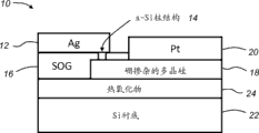
Fig. 1 (a) illustrates the nonvolatile solid state resistance device 10 that comprises nanoscale a-Si structure 14, described nanoscale a-Si structure 14 represents and can, by the resistance that is optionally set to a plurality of values and can be reset, all with suitable control circuit, carry out.Once be set up, resistance value can utilize small voltage to read, and described small voltage amplitude is enough to determine this resistance and does not make it change.Although the embodiment illustrating is used a-Si as resistive element, will be appreciated that, can use other amorphous silicon (nc-Si) structure, for example amorphous polysilicon.Therefore, as at this with used in the claims, amorphous silicon (nc-Si) represents to represent the amorphous silicon (a-Si) of controllable resistor or amorphous polysilicon (polycrystalline-Si) or described both combination.In addition, although many discussion here are also applied to more massive a-Si structure, for example those have the a-Si structure of one or more sizes in micrometer range, but the embodiment illustrating is a-Si nanostructure, described a-Si nanostructure represents the particular characteristics that only has its small size just to have.Just as used in this, term nanostructure refers to the structure with the size within the scope of at least two nanoscales; For example, there is diameter in the general range of 0.1 to 100 nanometer or the structure of a plurality of sectional dimensions.This comprises the structure with whole three nanoscale bulks; For example, have with its nanometer grade diameter in cylindrical nanometer bar or the nano-pillar of the length of identical magnitude.Nanostructure can comprise a plurality of nanostructure well known by persons skilled in the art; For example, nanotube, nano wire, nanometer rods, nano rod, nano-pillar, nano particle and nanofiber.Such structure 14 be Fig. 1 (a) and 1(b) shown in embodiment, described embodiment be cross section (have be less than 100 nm(for example shown in particular instance in be 60 nm) diameter) can be circular stopper or rod structure.Post height or length (depending on direction) can be nanoscales (being for example 30 nm in example illustrated) or larger.
Fig. 1 (a) and a-Si structure 14 1(b) are embedded in insulation dielectric 16, described insulation dielectric 16 can be made of a variety of materials and construct by different way, but shown in figure is spin-coating glass (SOG) layer 16, described spin-coating glass (SOG) layer 16 flows around a-Si structure 14 at first, then be cured, all these can utilize known technique to carry out.The layer-of-substrate silicon 22 that utilization is covered by hot dioxide layer 24 builds whole resistance device 10.Is boron doping or other p-type polysilicon electrode 18 that contacts and leave to hold from described post horizontal expansion stacked metal electrode 20 with the lower surface of a-Si post 14 below a-Si post 14, described metal electrode 20 can be made by any suitable metal (comprising for example platinum metal, such as palladium or platinum).The upper face (end face) of a-Si post 14 upper relative with polysilicon (p-Si) electrode 18 be silver (Ag) metal electrode 12 that serves as the source of filament formation ion.Although use in an illustrated embodiment silver, but should be understood that, this electrode 12(and another metal electrode 20) can be formed by multiple other suitable metal for example gold (Au), nickel (Ni), aluminium (Al), chromium (Cr), iron (Fe), manganese (Mn), tungsten (W), vanadium (V), cobalt (Co).Other suitable metal that can provide filament to form ion also can be provided.
For construction drawing 1(a) a-Si device 10, boron doping p-Si bottom electrode layer 18 can be by LPCVD(low-pressure chemical vapor deposition) be deposited on certified products (prime grade) silicon substrate with the hot dioxide of 200 nm.Amorphous silicon layer can be the thick layer of 30 nm that is deposited on the top of boron doped p-Si, after be two RIE(reactive ion etchings) step to be to limit a-Si post 14 and p-Si bottom electrode 18 structures.Then can, with the speed spin coating spin-coating glass (SOG) of 3000 RPM on sample, then it be solidified 1 hour at 320 ℃.This insulation SOG layer 16 provides the electricity isolation of two opposite electrodes 12,18 and provides mechanical support for a-Si post 14.After being formed, SOG layer 16 can be fallen to manufacture flat surfaces by partial etching and expose the end face of a-Si post 14.Then can utilize stripping technology to form Ag electrode 12 by being patterned on the end face of exposure of a-Si post 14.Then can apply the second metal (platinum) electrode 20 to be provided to the ohmic contact of bottom p-Si layer 18.Platinum electrode 20 makes the resistance minimum by p-Si electrode 18 with help near being positioned at a-Si post 14, and this distance is preferably not more than 100 nm.Can select design so as to minimize top and bottom electrode 12,18 between crossover to keep by the low DC leakage-current of SOG 16.It will be appreciated by those skilled in the art that and can carry out multiple modification to this fabrication schedule, and also can use other manufacture method to realize structure or the other suitable nc-Si structure of Fig. 1 (a) of the resistance adjustability that allows device.U.S. Patent Application Publication thing No. 2009/0014707 A1 provide relate to nonvolatile solid state resistor switching device (for example Fig. 1 (a) and 1(b) shown in a-Si device) characteristic, use and the additional information of operation.It also provides the information of the structure of the alternative embodiment that relates to a-Si device, its at least some applicable to Fig. 1 (a) with the structure of the a-Si device 1(b).At this, be incorporated to by reference the wherein information of manufacture, structure and the use of disclosed nonvolatile solid state resistor switching device that relates to being included in U.S. Patent Application Publication thing No. 2009/0014707 A1.
Single a-Si device shown in Fig. 1 (a) can be used as the interconnection of independent restructural or bank bit (utilize the controlled top of its independence and bottom electrode to).The polysilicon that uses chemical vapor deposition (CVD) deposition makes device can be manufactured on multiple substrate (comprise for multilayer 3D structure assembly may) as bottom contact.Compare with continuous a-Si film, the a-Si plug structure 14 illustrating contributes to guarantee active a-Si district and filament area are limited physically well.In addition, this structure of device and CMOS technology are completely compatible and for example can easily be incorporated to existing system, as the high-density nonvolatile memory in logical circuit (neuromorphic network) or restructural interconnection.
Fig. 1 (c) illustrates the resistance conversion characteristic (for example, for having the diameter of about 60 nm and the device of 30 nm thickness) of typical a-Si post (for example, shown in Fig. 1 (a)).It comprises the illustration that this conversion characteristics that is unit with logarithmic scale that the stepping during connection process changes is shown.These nanoscales a-Si switch does not need high pressure to form, and after formation described device can by apply just write and negative erasing voltage pulse low resistance connect and high resistance off-state between convert.The on/off resistance ratio of measuring under little biasing can be up to 10
7, as shown in Figure 1 (c).The test of the a-Si device of manufacturing in the above described manner shows, as memory device, with regard to rate of finished products (for example, for having rate of finished products >95% the device of a-Si post of 60 nm diameters), speed, durability and confining force, a-Si switch represents superior performance metric.Fig. 1 (d) illustrates that the representativeness with 50 ns write/erase pulse durations writes-read-wipe-read pulse train and from the output response of typical device.The result of the durability test of described device is shown in Fig. 1 (e).The typical device with the making current of < 20 μ A is expected to hold out against and is greater than 10
5individual programming cycle and not degenerating.Surpass this restriction, off-state electricity is led and is started to increase, thereby causes on/off resistance ratio to reduce.
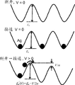
The conversion of a-Si structure can be explained by formation and the recovery of nanoscale Ag filament when applying program voltage, schematically illustrated in Fig. 2 (d).In the experiment and theoretical research about micron order metal/a-Si/ metal structure above, the Ag that filament is a succession of positively charged in the defective locations being captured in a-Si layer is proposed
+particle shape.Conductive mechanism in on-state is to pass through Ag
+the electron tunneling effect of chain, then device resistance is subject to last Ag
+tunnelling resistance domination between particle and bottom electrode.As shown in Figure 1 (c), the behavior with as additional Ag
+when particle hop increases in stepping mode to Ag filament in new trap sites, in the off-on transition period, take the stepping of the electric current that logarithmic scale is unit increases consistent.
The active domain transformation clearly limiting in a-Si rod structure makes it possible to study in great detail to explore together with the good control being provided by CMOS compatible fabrication technique the unique property being provided by resistor switching device.A direct result of filament formation model is that transformation ratio may be relevant to biasing, since different from electron tunneling effect, Ag
+the hop of particle is that thermal excitation process and this ratio are by the excitation energy relevant to biasing
e a ' (V)determine:

Wherein
k b be Boltzmann constant, T is absolute temperature, and τ is that the feature time of staying and ν are attempt frequencies.As shown in Figure 2 (d), can reduce excitation energy by applying bias voltage, cause producing stand-by period and the transformation ratio relevant to biasing.
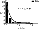
By the first research of changing the stand-by period of (being the first electric current step in Fig. 1 (c)) of the function to as bias voltage, verified this effect.By applying the rectangular pulse with given voltage amplitude to the decline of the device in off-state and measurement time t until first the increasing and measure the stand-by period rapidly of electric current.Then by negative voltage pulse, wipe described device and repeat described measurement.Fig. 2 (a)-(c) is illustrated on identity unit under the bias voltage of 2.6 V, 3.2 V and 3.6 V the histogram for the stand-by period of the first conversion.Because the random nature of conversion process, the stand-by period should be followed Poisson distribution and is in Δ at time t
tthe probability of interior appearance conversion is by providing below:

Histogram in Fig. 2 (a)-(c) can with equation 2 matchings of using τ as unique fitting parameter, thereby produce respectively the τ value of 15.3 ms, 1.2 ms and 0.029 ms.These figure show, τ is
vmajorant and
vwhile only increasing 1V, reduce about 10
3.Fig. 2 (e) is illustrated in the distribution of the τ measuring under 5 different bias voltages and the matching that adopts exponential decay, by τ
0 with
v 0 regard fitting parameter as:
(3)。
Interesting is to note in equation 3
v 0 physical significance.By Fig. 2 (d) and to the first rank,
 , wherein
e a activation energy while being zero offset,
ethat electric field and d are Ag
+distance between trap sites.If the major part of supposition voltage is fallen at Ag
+chain two ends and Ag
+particle is evenly distributed in chain, to the first rank
, wherein n is Ag
+the number of position.Then can directly derive
, wherein
e a activation energy while being zero offset,
ethat electric field and d are Ag
+distance between trap sites.If the major part of supposition voltage is fallen at Ag
+chain two ends and Ag
+particle is evenly distributed in chain, to the first rank
, wherein n is Ag
+the number of position.Then can directly derive equation 3 by equation 1, wherein


Importantly, the 0.155V's that the matching in Fig. 2 (e) is inferred
v 0 value is in close proximity to be concluded by this naive model
v 0 value,
 0.156V, supposes and in filament, has 3 Ag
+position (n=3), indicated as the main electric current number of steps in the semilog I-V curve in Fig. 1 (c).
0.156V, supposes and in filament, has 3 Ag
+position (n=3), indicated as the main electric current number of steps in the semilog I-V curve in Fig. 1 (c).Equation 3 clearly illustrates that, the stand-by period is relevant to biasing consumingly, and its biasing that can apply by increase and exponential form reduces.
The conversion characteristics relevant to biasing has important connotation to device operation.First, even if conversion may be very sharply-see Fig. 1 (c), conversion does not have " firmly " threshold voltage substantially yet, even because under relatively low bias voltage also federation occur the finite probability of conversion.On the other hand, threshold voltage can be defined for given programming pulse width.For example, if threshold value is restricted to the voltage that 95% success rate is implemented thereon, for 1 ms pulse threshold voltage, is 3.3 V, and is 5.1 V for the pulse-width threshold voltage of 10 ns.The second, by adjusting external circuit resistance, can in these devices, realize the storage of multistage position.When resistors in series is attached to device, the voltage at its two ends will be reduced after initial transformation, cause the stand-by period of conversion event subsequently more much longer.Therefore,, if removed programming pulse before conversion event subsequently may occur, the filament can generating portion forming, causes in the interlaminated resistance value switching on and off between state.Fig. 3 (a) is illustrated in and uses identical programming pulse still to have the last device resistance obtaining on the identity unit of different resistors in series values.On device, obtain 8=2
3individual different resistance values shows can store nearly 3 information as each device of memory unit.Device resistance R is also associated well with the resistance R s of resistors in series, as shown in Figure 3 (b), because cause that when device resistance becomes the voltage divider effect that the stand-by period extends is the most remarkable can compare with Rs time.
Several different methods can be used to realize multistage numeral is optionally programmed in a-Si device.Just as used in this, multistage numeral is to have the numeral that is greater than two (binary system) level or value, such as trit or numeral, quaternary numeral etc.Multistage stored digital can be used to store multidigit binary message; For example, level Four a-Si memory cell can be stored two bit binary data in single a-Si unit, and triad data can be stored in eight grades of unit.When using in digital circuit device, memory cell can comprise suitable control circuit with binary system or other digital programmable in a-Si device.Sort circuit in those skilled in the art's level and the exemplary schematic illustration of such control circuit shown in Figure 5.By additional resistance being inserted in the circuit of connecting with a-Si structure or by removing additional resistance in the circuit connecting with a-Si structure, shown control circuit can be used to a-Si structure to be arranged on any one of eight resistance stages.For this reason, can use decoding circuit that triad is inputted to data transformation becomes to be used for by control resistor place in circuit or the corresponding control signal that disconnects with circuit.Like this, decoding circuit can be by being arranged to the master control resistance of connecting with a-Si structure associated electrical resistance and the resistance of a-Si structure be adjusted to any one in a plurality of expectation resistance values.As what will recognize, the control circuit of Fig. 5 is only that the physical circuit of sketch and the resistance value that is used for writing, wipe and read a-Si structure arranges it is known to those skilled in the art.
For example the control circuit in Fig. 5 can be used to carry out above-mentioned a plurality of step to adjust the resistance of a-Si structure.These steps comprise the resistance that can be used for adjusting a-Si structure between the resistance value starting and last resistance value together.Conventionally, described method comprises a-Si structure (it is the first resistance device) and the second resistance device is electrically connected in series and executes alive step at the resistance device two ends that are connected in series.As mentioned above, the second resistance device is the controlling resistance that comprises the combination of one or two or more control resistors.According to the last resistance value of the expectation of a-Si structure, select (for example passing through decoding circuit) controlling resistance.And, as discussed herein, at least can be partly according to executing alive amplitude, executing the alive duration or according to both, the last resistance value of a-Si structure be set simultaneously.Therefore, apply step and can comprise that by the resistance device two ends being connected in series, applying the voltage of selected amplitude and duration arranges last resistance value.In addition, as mentioned above, can utilize a-Si structure to realize multistage stored digital, making last resistance value is in a plurality of optional resistance values.For this reason, step a-Si structure being electrically connected in series with controlling resistance further comprises that selecteed resistance value based in described optional resistance value is by optionally inserting or the one or more control resistors of connecting with a-Si structure of tap carry out formation control resistance in electricity.This again can utilize the decoding circuit of Fig. 5 or utilize apparent other appropriate circuitry to those skilled in the art to carry out.Resistance value for a-Si device is resetted and gets back to beginning, applies the resetting voltage of opposite polarity to a-Si structure.
A-Si structure can be used as having the memory cell of the digital nonvolatile semiconductor memory member of many a-Si memory cell of arranging with array or other suitable construction.Fig. 6 has described to be for example used to form the one exemplary embodiment of ultrahigh density storage device.The memory device 126 illustrating comprises having SiO
2the substrate 122 of top layer 124 with by one group of vertically superposed one group of cross bar structure that parallel p-Si electrode 118 forms of parallel metal electrode 112.A-Si resistance device (generally with 110 expressions) is positioned at each infall of two kinds of electrodes.The number elements that differs Fig. 6 of 100 with respect to the number elements of Fig. 1 can have the 26S Proteasome Structure and Function of the number elements that is similar to (yet not necessarily identical) Fig. 1.Resistance device 110 comprises the independent addressing storage cell of memory device 126.Is SOG or other insulating barrier 116 that comprises a-Si structure at each memory cell 110 place between upper electrode group 112 and lower electrode group 118.Insulating barrier 116 can extend downwardly into the upper strata 124 of substrate and therefore isolate electrode adjacent one another are 118, or can use minute used outside insulated layer 121 below layer 116 for this reason.And, be not between the adjacent cells in row, to extend p-Si electrode 118, but the p-Si electrode that they can be limited to each cell position and can interconnect in every row with Pt or other suitable metal electrode.Other modification to those skilled in the art will be apparent.The cell size 127 of device 110 is approximately 0.003 μ m
2.In other example, cell size 127 can be less than 0.003 μ m
2or be less than or equal to 0.01 μ m
2.
Each memory cell 110 can comprise single a-Si structure, and as mentioned above, a-Si structure can have the adjustable resistance that is used to realize one-bit digital storage, maybe can have any one adjustable resistance being set in three or more resistance (its each corresponding to different storage numerals).Like this, each memory cell can be carried out multistage stored digital.For this reason, memory cell 126 can comprise that control circuit in Fig. 5 is for example to allow writing multi-stage data at any selected memory cell 110 places.
A-Si structure can operate switching on and off the method that converts it between state by above-mentioned, rather than is used to position or multistage stored digital.This can be undertaken by applying voltage at a-Si structure two ends, and the voltage wherein applying has selected to realize a-Si device transforms to the predetermined probability of on-state amplitude and the duration from off-state.The predetermined probability of successful transformation can be for example 95% or can be any other percentage that the special applications of a-Si device is desired or require.
As noted above, the amplitude of biasing is not only depended in the successful operation of a-Si device, and depends on the duration of biasing.What expectation was also depended in conversion control requirement is digital conversion (for example, as a bit memory) or simulated operation (for example, as interconnection).For Poisson process discussed above, Fig. 3 (c) is depicted in a probability that conversion event just in time occurs during time t, and Fig. 3 (d) is depicted in the probability that at least one conversion event occurs during time t.They are corresponding to not having situation and single interconversion rate 1/ τ of outside series resistance to be applicable to stepping filament forming process.Then it is apparent that, for device described in sufficiently long programming pulse serve as fabulous digital switch (for example for
t pulse > 3 τ
,obtain 95% success rate).On the other hand, for multistage stored digital or the simulated operation of switch, pulse duration must be optimised.For example, for the maximum probability that only the first conversion occurs,
t pulse must τ center.Even so, maximum success rate is only 38%, as shown in Figure 3 (c).Yet, can obviously improve by additional external series resistance the success rate of multi-position action, it has reduced interconversion rate subsequently significantly.Fig. 3 (e) draws the probability that only the first conversion event occurs in the two step filament forming processes (wherein using two different ratios) of simplifying:

τ wherein
1 =3.36 μ s and τ
2 =1.30 s correspond respectively to voltage when device two ends from 4V(before the first conversion event and R >> R
s) change to 2 V(after the first conversion event and R=R
s) time interconversion rate, as the result of voltage divider effect after the first conversion event.Now for 5 τ
1 <
t pulse <0.01 τ
2 (time margin of about 13 ms under 4 V biasings) can realize be greater than 99% more much higher success rate with by Transform Limited to the first event only.In addition, the characteristic similarly representing is expected from other resistor switching device, for example, because many certain activation energy processes (diffusion of ion and redox reaction) that comprise in them.
Temperature that can be relevant by the stand-by period to equation 1 is obtained the activation energy of potential barrier.Fig. 4 (a) illustrate the device that is programmed in on-state at first under zero offset under the temperature from 100 ℃ to 150 ℃ with the resistance variations of time correlation.Referring back to Fig. 1 (c), to the unexpected conversion of off-state, corresponding to the recovery of Ag filament, (pass through Ag
+particle is from the trap sites that approaches most bottom electrode to top electrodes hot activation hop), as passing through the stand-by period t and 1/ shown in Fig. 4 (b)
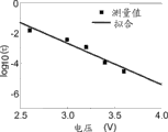
k b tarrhenius type relation curve in good fit checked.According to Arrhenius slope of a curve, it is 0.87 eV that the activation energy of the on/off of described device conversion can be obtained, and can estimatedly be 6 years according to extrapolation retention time at room temperature.
When being merged in example as shown in Figure 6 during memory array or in addition when special applications needs or during expectation, can utilize with the intrinsic diode of p-n junction form and construct described a-Si device.For example, by further comprise N-shaped layer between p-type polysilicon electrode and the second metal (platinum) electrode, described a-Si device can be merged in during manufacture.Above-mentioned example is shown in Figure 7, and the N-shaped layer increasing under Pt electrode, it can be identical with the a-Si resistance device 10 of Fig. 1.While using in the memory array at intersection stripe shape, this structure can be used to prevent crosstalking between adjacent devices, because the conduction current forward that flows out a unit by its diode will be stopped by the diode of adjacent cells (being reverse biased now).
Fig. 8 has described to comprise another embodiment of the single unit a-Si resistance device 210 of diode-built-in, and it can utilize conventional cmos manufacturing technology to form.The number elements that differs Fig. 8 of 200 with respect to the number elements of Fig. 1 can have the similar 26S Proteasome Structure and Function of number elements (yet not necessarily identical) with Fig. 1.Device 210 can utilize N-type crystalline silicon substrate 222 structures.P type silicon area 218 can be the polysilicon layer for example, forming by stand CMOS (Implantation or method of diffusion).Territory, p type island region 218 contacts with a-Si post 214 with Ag terminal 212, and it can change its resistance according to the biasing applying, as mentioned above.Can pass through SOG(spin-coating glass) or CVD(chemical vapour deposition (CVD)) method formation insulating barrier 216.The second metal electrode 220 is formed to such an extent that contact with substrate layer 222, and can be that for example to have the TiN/Al of good electric contact metal laminated.Highly doped N-type region 226(can form by Implantation it) further guarantee the excellent electric contact between N substrate 222 and electrode 220.Because P type layer 218 is structured on N-type silicon substrate 222, they form diode together.Therefore,, when electrode 212 and 220 is during for external contact, total comprises the a-Si resistance device with the PN diode being connected in series.Fig. 9 has described to be similar to the structure 310 of Fig. 8, and main difference is the type (it can be p-type substrate 318) that starts substrate.In this case, then N-type region 222 is formed on (by Implantation or method of diffusion) on substrate 218, and it provides the PN being connected in series diode again to a-Si resistance device.
Figure 10 has described an exemplary embodiment of a-Si resistance device 400, thereby described a-Si resistance device 400 comprises that some are used to a-Si outline programming to allow multidigit in device or the control circuit of other multistage stored digital to any one in much different resistance.This structure 400 can be constructed by conventional cmos manufacturing process.Described textural association a-Si resistance device 402(there is PN diode) and can serve as the FET 404 of gate bias control resistor.A-Si device 402 comprises the a-Si nano-pillar 414 in the insulating barrier 416 embedding under top electrodes, and described top electrodes can be silver or other suitable metal.FET 404 comprises the grid 430 that are formed on gate oxide 432.Depend on the biasing applying at grid 430, thereby the resistance between two N-type regions 423,425 can be controlled generation variable resistance.N-type region 425 is connected to the second metal electrode 420 by highly doped N-type region 427.Structure 400 can be fabricated on P type silicon substrate 418.Another territory, p type island region 421 has the resistance value different from P substrate 418 with control device performance.Polysilicon interconnection 450 comes bridge joint a-Si resistance device 402 and N-type FET 404 by connecting two N-type regions 422,423.STI(shallow trench isolation from) the 440th, standard CMOS manufacturing technology, it can suppress by the DC leakage-current of P substrate 418.If the thin thickness of active substrates (body) (< 1 μ m), the structure of device 400 can be simplified as shown in Figure 11.This consists essentially of from the device 400 of Figure 10 and removes element 440,450 and 423.Substrate 518 can be P type silicon.N-type region 522 can, as the N part of PN diode and a part of FET, cause forming compact device size.
Except using the N-shaped layer increasing to create above-mentioned diode-built-in, basic a-Si resistance device disclosed herein itself just can represent intrinsic diode characteristic.Figure 12 and 13 illustrates the example of this diode characteristic.As shown in these figures, when the on-state of memory device in it, electric current can be only under positive bias and do not flow through device under negative bias.This intrinsic diode characteristic also can be used to regulate current flowing and prevent crosstalking in cross bar array.Can be by controlling a-Si sedimentary condition and/or obtaining intrinsic diode characteristic by controlling program current.In the situation that not wishing to be limited to any special operational theory, the possible cause that will be understood that this intrinsic property is the shallow trap electromotive force between the internal electric field of interface and/or PECVD a-Si/ polysilicon.Utilization is than the common programming much smaller biasing of setovering, and the Ag mobile ion naturally retracting can be injected into approaching interface again, therefore when utilizing, little still can obtain on-state when just reading voltage and reading device state.This process is different from erase process, and wherein Ag mobile ion is pulled back to another settling position with enough barrier energies.
It will be understood that, aforementioned is the description of one or more preferred one exemplary embodiment of the present invention.The present invention is not limited to specific embodiment disclosed herein, but only by claim below, is limited.In addition, be included in the restriction that statement in describing above relates to specific embodiment and is not counted as the definition of the term to using in scope of the present invention or claim, unless wherein term or phrase are clearly limited in the above.Various other embodiment and becoming apparent those skilled in the art the various changes of disclosed embodiment or modification.All such other embodiment, change and modification are intended to be included in the scope of claims.
As what use in this specification and claim, when in conjunction with one or more parts or other list use, term " for example ", " for instance ", " such as " and " similar " and verb " comprises ", " having ", " comprising " and their other verb form are all understood to open, the meaning be described list by be not understood to get rid of other, other parts or.Other will utilize they the most rationally meaning explain, unless they use in the different contexts of explaining of needs.
Claims (19)
1. a nonvolatile solid state resistance device, comprising:
The first metal electrode;
P-type polysilicon electrode;
Insulating barrier between described electrode at least in part;
Embed in described insulating barrier and there is the amorphous silicon structures of the opposing end surface that is all connected to the Different electrodes in described electrode, wherein said the first metal electrode comprises metal, described metal is in the situation that described electrode two ends exist the voltage applying that the metal ion that forms filament in described amorphous silicon structures is provided, thus, show can be according to the controlled resistance of the voltage applying for described amorphous silicon structures; And
The second metal electrode contacting with described polysilicon electrode in the position that is no more than 100 nm from described amorphous silicon structures.
2. resistance device as described in claim 1, wherein said insulating barrier comprises spin-on-glass layer.
3. resistance device as described in claim 1, wherein said amorphous silicon structures comprises the post with opposing end surface, and each electrode and different end contacts in described end face.
4. resistance device as described in claim 1, wherein said amorphous silicon structures is all nanoscale in all three bulks.
5. resistance device as described in claim 4, each in wherein said size is less than 100 nm.
6. resistance device as described in claim 1, further comprises the resistance component that one or more and described amorphous silicon structures electricity is connected in series.
7. resistance device as described in claim 6, wherein said resistance component comprises control resistor.
8. resistance device as described in claim 7, further comprises control circuit, and described control circuit comprises described one or more resistance component, and for optionally changing the circuit of the quantity of the series resistance that is connected to described amorphous silicon structures.
9. resistance device as described in claim 1, further comprises for adjust the control circuit of the resistance of described amorphous silicon structures between plural resistance value.
10. resistance device as described in claim 9, wherein said control circuit provides the controlling resistance being connected in series with described amorphous silicon structures, and described control circuit is used for by controlling resistance being set to any one that associated electrical resistance is adjusted to the resistance of amorphous silicon structures described resistance value.
11. resistance devices as described in claim 1, further comprise the N-shaped doped silicon layer contacting with described p-type polysilicon electrode, make described resistance device comprise the diode of connecting with described amorphous silicon structures.
12. resistance devices as described in claim 1, wherein said the first metal electrode comprises silver.
13. resistance devices as described in claim 1, are further included near the second metal electrode that position contacts with described p-type polysilicon electrode described amorphous silicon structures.
14. resistance devices as described in claim 13, wherein said the second metal electrode and described amorphous silicon structures interval are no more than 100 nm.
A 15. digital nonvolatile semiconductor memory member with at least one memory cell that comprises the resistance device described in claim 1.
16. memory devices as described in claim 15, the amorphous silicon structures of wherein said resistance device is the unique amorphous silicon structures having in the described memory cell of adjustable resistance, and wherein adjustable resistance can be set to any one in three or more resistance, each in described three or more resistance is corresponding to different storage numerals, and described memory cell can be carried out multistage stored digital thus.
17. memory devices as described in claim 16, further comprise for according to the numeral of storing is arranged to the control circuit of adjustable electric resistance in memory cell.
18. memory devices as described in claim 17, wherein control circuit comprises the controlling resistance of connecting with described amorphous silicon structures.
19. 1 kinds of electronic circuits with the electrical interconnection that comprises the resistance device described in claim 1.
Applications Claiming Priority (3)
| Application Number | Priority Date | Filing Date | Title |
|---|---|---|---|
| US10392808P | 2008-10-08 | 2008-10-08 | |
| US61/103928 | 2008-10-08 | ||
| PCT/US2009/060023 WO2010042732A2 (en) | 2008-10-08 | 2009-10-08 | Silicon-based nanoscale resistive device with adjustable resistance |
Publications (2)
| Publication Number | Publication Date |
|---|---|
| CN102177584A CN102177584A (en) | 2011-09-07 |
| CN102177584B true CN102177584B (en) | 2014-05-07 |
Family
ID=42075693
Family Applications (1)
| Application Number | Title | Priority Date | Filing Date |
|---|---|---|---|
| CN200980139738.3A Expired - Fee Related CN102177584B (en) | 2008-10-08 | 2009-10-08 | Silicon-based nanoscale resistive device with adjustable resistance |
Country Status (6)
| Country | Link |
|---|---|
| US (2) | US8687402B2 (en) |
| EP (1) | EP2342750B1 (en) |
| JP (1) | JP5702725B2 (en) |
| KR (1) | KR20110080153A (en) |
| CN (1) | CN102177584B (en) |
| WO (1) | WO2010042732A2 (en) |
Families Citing this family (141)
| Publication number | Priority date | Publication date | Assignee | Title |
|---|---|---|---|---|
| US7768812B2 (en) | 2008-01-15 | 2010-08-03 | Micron Technology, Inc. | Memory cells, memory cell programming methods, memory cell reading methods, memory cell operating methods, and memory devices |
| US8034655B2 (en) | 2008-04-08 | 2011-10-11 | Micron Technology, Inc. | Non-volatile resistive oxide memory cells, non-volatile resistive oxide memory arrays, and methods of forming non-volatile resistive oxide memory cells and memory arrays |
| US8211743B2 (en) | 2008-05-02 | 2012-07-03 | Micron Technology, Inc. | Methods of forming non-volatile memory cells having multi-resistive state material between conductive electrodes |
| US8134137B2 (en) | 2008-06-18 | 2012-03-13 | Micron Technology, Inc. | Memory device constructions, memory cell forming methods, and semiconductor construction forming methods |
| US9343665B2 (en) | 2008-07-02 | 2016-05-17 | Micron Technology, Inc. | Methods of forming a non-volatile resistive oxide memory cell and methods of forming a non-volatile resistive oxide memory array |
| JP2012506621A (en) | 2008-10-20 | 2012-03-15 | ザ・リージェンツ・オブ・ザ・ユニバーシティ・オブ・ミシガン | Silicon nanoscale crossbar memory |
| JP5543819B2 (en) | 2010-03-26 | 2014-07-09 | 株式会社東芝 | Resistance change element, memory cell array, and resistance change device |
| US8427859B2 (en) | 2010-04-22 | 2013-04-23 | Micron Technology, Inc. | Arrays of vertically stacked tiers of non-volatile cross point memory cells, methods of forming arrays of vertically stacked tiers of non-volatile cross point memory cells, and methods of reading a data value stored by an array of vertically stacked tiers of non-volatile cross point memory cells |
| US8411477B2 (en) | 2010-04-22 | 2013-04-02 | Micron Technology, Inc. | Arrays of vertically stacked tiers of non-volatile cross point memory cells, methods of forming arrays of vertically stacked tiers of non-volatile cross point memory cells, and methods of reading a data value stored by an array of vertically stacked tiers of non-volatile cross point memory cells |
| US8289763B2 (en) | 2010-06-07 | 2012-10-16 | Micron Technology, Inc. | Memory arrays |
| US9601692B1 (en) | 2010-07-13 | 2017-03-21 | Crossbar, Inc. | Hetero-switching layer in a RRAM device and method |
| US9012307B2 (en) * | 2010-07-13 | 2015-04-21 | Crossbar, Inc. | Two terminal resistive switching device structure and method of fabricating |
| US9570678B1 (en) | 2010-06-08 | 2017-02-14 | Crossbar, Inc. | Resistive RAM with preferental filament formation region and methods |
| US8946046B1 (en) | 2012-05-02 | 2015-02-03 | Crossbar, Inc. | Guided path for forming a conductive filament in RRAM |
| US8780601B2 (en) * | 2010-06-08 | 2014-07-15 | Hewlett-Packard Development Company, L.P. | Three-dimensional integrated circuit |
| KR101883236B1 (en) | 2010-06-11 | 2018-08-01 | 크로스바, 인크. | Pillar structure for memory device and method |
| US8441835B2 (en) | 2010-06-11 | 2013-05-14 | Crossbar, Inc. | Interface control for improved switching in RRAM |
| US8374018B2 (en) | 2010-07-09 | 2013-02-12 | Crossbar, Inc. | Resistive memory using SiGe material |
| US8467227B1 (en) | 2010-11-04 | 2013-06-18 | Crossbar, Inc. | Hetero resistive switching material layer in RRAM device and method |
| US8884261B2 (en) | 2010-08-23 | 2014-11-11 | Crossbar, Inc. | Device switching using layered device structure |
| US8947908B2 (en) | 2010-11-04 | 2015-02-03 | Crossbar, Inc. | Hetero-switching layer in a RRAM device and method |
| US8569172B1 (en) | 2012-08-14 | 2013-10-29 | Crossbar, Inc. | Noble metal/non-noble metal electrode for RRAM applications |
| US8168506B2 (en) | 2010-07-13 | 2012-05-01 | Crossbar, Inc. | On/off ratio for non-volatile memory device and method |
| US9224496B2 (en) | 2010-08-11 | 2015-12-29 | Shine C. Chung | Circuit and system of aggregated area anti-fuse in CMOS processes |
| US10229746B2 (en) | 2010-08-20 | 2019-03-12 | Attopsemi Technology Co., Ltd | OTP memory with high data security |
| US9236141B2 (en) | 2010-08-20 | 2016-01-12 | Shine C. Chung | Circuit and system of using junction diode of MOS as program selector for programmable resistive devices |
| US9431127B2 (en) | 2010-08-20 | 2016-08-30 | Shine C. Chung | Circuit and system of using junction diode as program selector for metal fuses for one-time programmable devices |
| US9496033B2 (en) | 2010-08-20 | 2016-11-15 | Attopsemi Technology Co., Ltd | Method and system of programmable resistive devices with read capability using a low supply voltage |
| US10249379B2 (en) | 2010-08-20 | 2019-04-02 | Attopsemi Technology Co., Ltd | One-time programmable devices having program selector for electrical fuses with extended area |
| US9251893B2 (en) | 2010-08-20 | 2016-02-02 | Shine C. Chung | Multiple-bit programmable resistive memory using diode as program selector |
| US9019742B2 (en) | 2010-08-20 | 2015-04-28 | Shine C. Chung | Multiple-state one-time programmable (OTP) memory to function as multi-time programmable (MTP) memory |
| US9025357B2 (en) | 2010-08-20 | 2015-05-05 | Shine C. Chung | Programmable resistive memory unit with data and reference cells |
| US9070437B2 (en) | 2010-08-20 | 2015-06-30 | Shine C. Chung | Circuit and system of using junction diode as program selector for one-time programmable devices with heat sink |
| US9711237B2 (en) | 2010-08-20 | 2017-07-18 | Attopsemi Technology Co., Ltd. | Method and structure for reliable electrical fuse programming |
| US8929122B2 (en) | 2010-08-20 | 2015-01-06 | Shine C. Chung | Circuit and system of using a junction diode as program selector for resistive devices |
| US10923204B2 (en) | 2010-08-20 | 2021-02-16 | Attopsemi Technology Co., Ltd | Fully testible OTP memory |
| US9824768B2 (en) | 2015-03-22 | 2017-11-21 | Attopsemi Technology Co., Ltd | Integrated OTP memory for providing MTP memory |
| US10916317B2 (en) | 2010-08-20 | 2021-02-09 | Attopsemi Technology Co., Ltd | Programmable resistance memory on thin film transistor technology |
| US9460807B2 (en) | 2010-08-20 | 2016-10-04 | Shine C. Chung | One-time programmable memory devices using FinFET technology |
| US9042153B2 (en) | 2010-08-20 | 2015-05-26 | Shine C. Chung | Programmable resistive memory unit with multiple cells to improve yield and reliability |
| US9818478B2 (en) | 2012-12-07 | 2017-11-14 | Attopsemi Technology Co., Ltd | Programmable resistive device and memory using diode as selector |
| US8889521B1 (en) | 2012-09-14 | 2014-11-18 | Crossbar, Inc. | Method for silver deposition for a non-volatile memory device |
| US8492195B2 (en) | 2010-08-23 | 2013-07-23 | Crossbar, Inc. | Method for forming stackable non-volatile resistive switching memory devices |
| US9401475B1 (en) | 2010-08-23 | 2016-07-26 | Crossbar, Inc. | Method for silver deposition for a non-volatile memory device |
| US8841196B1 (en) | 2010-09-29 | 2014-09-23 | Crossbar, Inc. | Selective deposition of silver for non-volatile memory device fabrication |
| US8404553B2 (en) | 2010-08-23 | 2013-03-26 | Crossbar, Inc. | Disturb-resistant non-volatile memory device and method |
| US8351242B2 (en) | 2010-09-29 | 2013-01-08 | Micron Technology, Inc. | Electronic devices, memory devices and memory arrays |
| US8391049B2 (en) | 2010-09-29 | 2013-03-05 | Crossbar, Inc. | Resistor structure for a non-volatile memory device and method |
| US8558212B2 (en) | 2010-09-29 | 2013-10-15 | Crossbar, Inc. | Conductive path in switching material in a resistive random access memory device and control |
| US8723154B2 (en) * | 2010-09-29 | 2014-05-13 | Crossbar, Inc. | Integration of an amorphous silicon resistive switching device |
| US8759809B2 (en) | 2010-10-21 | 2014-06-24 | Micron Technology, Inc. | Integrated circuitry comprising nonvolatile memory cells having platelike electrode and ion conductive material layer |
| US8187945B2 (en) | 2010-10-27 | 2012-05-29 | Crossbar, Inc. | Method for obtaining smooth, continuous silver film |
| US8526213B2 (en) | 2010-11-01 | 2013-09-03 | Micron Technology, Inc. | Memory cells, methods of programming memory cells, and methods of forming memory cells |
| US8796661B2 (en) | 2010-11-01 | 2014-08-05 | Micron Technology, Inc. | Nonvolatile memory cells and methods of forming nonvolatile memory cell |
| US8923085B2 (en) | 2010-11-03 | 2014-12-30 | Shine C. Chung | Low-pin-count non-volatile memory embedded in a integrated circuit without any additional pins for access |
| US8988965B2 (en) | 2010-11-03 | 2015-03-24 | Shine C. Chung | Low-pin-count non-volatile memory interface |
| US9019791B2 (en) | 2010-11-03 | 2015-04-28 | Shine C. Chung | Low-pin-count non-volatile memory interface for 3D IC |
| US8258020B2 (en) | 2010-11-04 | 2012-09-04 | Crossbar Inc. | Interconnects for stacked non-volatile memory device and method |
| US8502185B2 (en) | 2011-05-31 | 2013-08-06 | Crossbar, Inc. | Switching device having a non-linear element |
| USRE46335E1 (en) | 2010-11-04 | 2017-03-07 | Crossbar, Inc. | Switching device having a non-linear element |
| US8088688B1 (en) | 2010-11-05 | 2012-01-03 | Crossbar, Inc. | p+ polysilicon material on aluminum for non-volatile memory device and method |
| US9454997B2 (en) | 2010-12-02 | 2016-09-27 | Micron Technology, Inc. | Array of nonvolatile memory cells having at least five memory cells per unit cell, having a plurality of the unit cells which individually comprise three elevational regions of programmable material, and/or having a continuous volume having a combination of a plurality of vertically oriented memory cells and a plurality of horizontally oriented memory cells; array of vertically stacked tiers of nonvolatile memory cells |
| US9496265B2 (en) | 2010-12-08 | 2016-11-15 | Attopsemi Technology Co., Ltd | Circuit and system of a high density anti-fuse |
| US8431458B2 (en) | 2010-12-27 | 2013-04-30 | Micron Technology, Inc. | Methods of forming a nonvolatile memory cell and methods of forming an array of nonvolatile memory cells |
| US8930174B2 (en) | 2010-12-28 | 2015-01-06 | Crossbar, Inc. | Modeling technique for resistive random access memory (RRAM) cells |
| US8815696B1 (en) | 2010-12-31 | 2014-08-26 | Crossbar, Inc. | Disturb-resistant non-volatile memory device using via-fill and etchback technique |
| US9153623B1 (en) | 2010-12-31 | 2015-10-06 | Crossbar, Inc. | Thin film transistor steering element for a non-volatile memory device |
| US8791010B1 (en) | 2010-12-31 | 2014-07-29 | Crossbar, Inc. | Silver interconnects for stacked non-volatile memory device and method |
| US8791447B2 (en) | 2011-01-20 | 2014-07-29 | Micron Technology, Inc. | Arrays of nonvolatile memory cells and methods of forming arrays of nonvolatile memory cells |
| US10586832B2 (en) | 2011-02-14 | 2020-03-10 | Attopsemi Technology Co., Ltd | One-time programmable devices using gate-all-around structures |
| US10192615B2 (en) | 2011-02-14 | 2019-01-29 | Attopsemi Technology Co., Ltd | One-time programmable devices having a semiconductor fin structure with a divided active region |
| US8848423B2 (en) | 2011-02-14 | 2014-09-30 | Shine C. Chung | Circuit and system of using FinFET for building programmable resistive devices |
| US8488365B2 (en) | 2011-02-24 | 2013-07-16 | Micron Technology, Inc. | Memory cells |
| JP5439420B2 (en) * | 2011-03-22 | 2014-03-12 | 株式会社東芝 | Storage device |
| US8537592B2 (en) | 2011-04-15 | 2013-09-17 | Micron Technology, Inc. | Arrays of nonvolatile memory cells and methods of forming arrays of nonvolatile memory cells |
| US8450710B2 (en) | 2011-05-27 | 2013-05-28 | Crossbar, Inc. | Low temperature p+ silicon junction material for a non-volatile memory device |
| US8394670B2 (en) | 2011-05-31 | 2013-03-12 | Crossbar, Inc. | Vertical diodes for non-volatile memory device |
| US9620206B2 (en) | 2011-05-31 | 2017-04-11 | Crossbar, Inc. | Memory array architecture with two-terminal memory cells |
| JP2013004143A (en) * | 2011-06-16 | 2013-01-07 | Toshiba Corp | Nonvolatile semiconductor memory device |
| US8619459B1 (en) | 2011-06-23 | 2013-12-31 | Crossbar, Inc. | High operating speed resistive random access memory |
| US8659929B2 (en) | 2011-06-30 | 2014-02-25 | Crossbar, Inc. | Amorphous silicon RRAM with non-linear device and operation |
| US9564587B1 (en) | 2011-06-30 | 2017-02-07 | Crossbar, Inc. | Three-dimensional two-terminal memory with enhanced electric field and segmented interconnects |
| US9627443B2 (en) | 2011-06-30 | 2017-04-18 | Crossbar, Inc. | Three-dimensional oblique two-terminal memory with enhanced electric field |
| US9166163B2 (en) | 2011-06-30 | 2015-10-20 | Crossbar, Inc. | Sub-oxide interface layer for two-terminal memory |
| US8946669B1 (en) | 2012-04-05 | 2015-02-03 | Crossbar, Inc. | Resistive memory device and fabrication methods |
| WO2013015776A1 (en) | 2011-07-22 | 2013-01-31 | Crossbar, Inc. | Seed layer for a p + silicon germanium material for a non-volatile memory device and method |
| US10056907B1 (en) | 2011-07-29 | 2018-08-21 | Crossbar, Inc. | Field programmable gate array utilizing two-terminal non-volatile memory |
| US9729155B2 (en) | 2011-07-29 | 2017-08-08 | Crossbar, Inc. | Field programmable gate array utilizing two-terminal non-volatile memory |
| US8674724B2 (en) | 2011-07-29 | 2014-03-18 | Crossbar, Inc. | Field programmable gate array utilizing two-terminal non-volatile memory |
| JP5548170B2 (en) | 2011-08-09 | 2014-07-16 | 株式会社東芝 | Resistance change memory and manufacturing method thereof |
| JP5537524B2 (en) | 2011-09-22 | 2014-07-02 | 株式会社東芝 | Resistance change memory |
| US9324849B2 (en) | 2011-11-15 | 2016-04-26 | Shine C. Chung | Structures and techniques for using semiconductor body to construct SCR, DIAC, or TRIAC |
| US9136261B2 (en) | 2011-11-15 | 2015-09-15 | Shine C. Chung | Structures and techniques for using mesh-structure diodes for electro-static discharge (ESD) protection |
| JP5798052B2 (en) * | 2012-01-31 | 2015-10-21 | 株式会社東芝 | Storage device |
| JP5634426B2 (en) * | 2012-03-22 | 2014-12-03 | 株式会社東芝 | Storage device |
| US9007804B2 (en) * | 2012-02-06 | 2015-04-14 | Shine C. Chung | Circuit and system of protective mechanisms for programmable resistive memories |
| US8975727B2 (en) | 2012-02-28 | 2015-03-10 | Intermolecular, Inc. | Memory cell having an integrated two-terminal current limiting resistor |
| US8716098B1 (en) | 2012-03-09 | 2014-05-06 | Crossbar, Inc. | Selective removal method and structure of silver in resistive switching device for a non-volatile memory device |
| US9087576B1 (en) | 2012-03-29 | 2015-07-21 | Crossbar, Inc. | Low temperature fabrication method for a three-dimensional memory device and structure |
| US8946667B1 (en) | 2012-04-13 | 2015-02-03 | Crossbar, Inc. | Barrier structure for a silver based RRAM and method |
| US9685608B2 (en) | 2012-04-13 | 2017-06-20 | Crossbar, Inc. | Reduced diffusion in metal electrode for two-terminal memory |
| US8658476B1 (en) | 2012-04-20 | 2014-02-25 | Crossbar, Inc. | Low temperature P+ polycrystalline silicon material for non-volatile memory device |
| US8796658B1 (en) | 2012-05-07 | 2014-08-05 | Crossbar, Inc. | Filamentary based non-volatile resistive memory device and method |
| US8765566B2 (en) | 2012-05-10 | 2014-07-01 | Crossbar, Inc. | Line and space architecture for a non-volatile memory device |
| US9070859B1 (en) | 2012-05-25 | 2015-06-30 | Crossbar, Inc. | Low temperature deposition method for polycrystalline silicon material for a non-volatile memory device |
| JP5783961B2 (en) * | 2012-07-09 | 2015-09-24 | 株式会社東芝 | Nonvolatile memory device |
| WO2014018318A1 (en) * | 2012-07-27 | 2014-01-30 | Tactonic Technologies, Llc | Method for mechanical sensing utilizing controlled current |
| US10096653B2 (en) | 2012-08-14 | 2018-10-09 | Crossbar, Inc. | Monolithically integrated resistive memory using integrated-circuit foundry compatible processes |
| US9583701B1 (en) | 2012-08-14 | 2017-02-28 | Crossbar, Inc. | Methods for fabricating resistive memory device switching material using ion implantation |
| US20140050010A1 (en) * | 2012-08-15 | 2014-02-20 | Kabushiki Kaisha Toshiba | Semiconductor memory device and file memory system |
| US8946673B1 (en) | 2012-08-24 | 2015-02-03 | Crossbar, Inc. | Resistive switching device structure with improved data retention for non-volatile memory device and method |
| US8796102B1 (en) | 2012-08-29 | 2014-08-05 | Crossbar, Inc. | Device structure for a RRAM and method |
| US9076526B2 (en) | 2012-09-10 | 2015-07-07 | Shine C. Chung | OTP memories functioning as an MTP memory |
| US9312483B2 (en) | 2012-09-24 | 2016-04-12 | Crossbar, Inc. | Electrode structure for a non-volatile memory device and method |
| US9183897B2 (en) | 2012-09-30 | 2015-11-10 | Shine C. Chung | Circuits and methods of a self-timed high speed SRAM |
| US9576616B2 (en) | 2012-10-10 | 2017-02-21 | Crossbar, Inc. | Non-volatile memory with overwrite capability and low write amplification |
| US11068620B2 (en) | 2012-11-09 | 2021-07-20 | Crossbar, Inc. | Secure circuit integrated with memory layer |
| US8982647B2 (en) | 2012-11-14 | 2015-03-17 | Crossbar, Inc. | Resistive random access memory equalization and sensing |
| US9324447B2 (en) | 2012-11-20 | 2016-04-26 | Shine C. Chung | Circuit and system for concurrently programming multiple bits of OTP memory devices |
| US9412790B1 (en) | 2012-12-04 | 2016-08-09 | Crossbar, Inc. | Scalable RRAM device architecture for a non-volatile memory device and method |
| US8890109B2 (en) * | 2012-12-20 | 2014-11-18 | Intermolecular, Inc. | Resistive random access memory access cells having thermally isolating structures |
| US9406379B2 (en) | 2013-01-03 | 2016-08-02 | Crossbar, Inc. | Resistive random access memory with non-linear current-voltage relationship |
| US9112145B1 (en) | 2013-01-31 | 2015-08-18 | Crossbar, Inc. | Rectified switching of two-terminal memory via real time filament formation |
| US9324942B1 (en) | 2013-01-31 | 2016-04-26 | Crossbar, Inc. | Resistive memory cell with solid state diode |
| US8934280B1 (en) | 2013-02-06 | 2015-01-13 | Crossbar, Inc. | Capacitive discharge programming for two-terminal memory cells |
| US9093635B2 (en) | 2013-03-14 | 2015-07-28 | Crossbar, Inc. | Controlling on-state current for two-terminal memory |
| US9099645B2 (en) | 2013-03-22 | 2015-08-04 | Kabushiki Kaisha Toshiba | Resistance random access memory device |
| US8860182B1 (en) | 2013-03-22 | 2014-10-14 | Kabushiki Kaisha Toshiba | Resistance random access memory device |
| US20150129829A1 (en) * | 2013-11-13 | 2015-05-14 | Crossbar, Inc. | One time programmable and multi-level, two-terminal memory cell |
| US10290801B2 (en) | 2014-02-07 | 2019-05-14 | Crossbar, Inc. | Scalable silicon based resistive memory device |
| CN103996790B (en) * | 2014-05-28 | 2016-10-05 | 河北大学 | A kind of nanoscale tri-state resistance-variable storing device and preparation method thereof |
| US9412473B2 (en) | 2014-06-16 | 2016-08-09 | Shine C. Chung | System and method of a novel redundancy scheme for OTP |
| KR102140787B1 (en) * | 2014-07-07 | 2020-08-03 | 삼성전자주식회사 | Resistive Memory Device and Operating Method thereof |
| CN104916380A (en) * | 2015-05-11 | 2015-09-16 | 岳文智 | Low voltage variable resistor |
| CN105372849B (en) * | 2015-11-27 | 2018-08-24 | 电子科技大学 | A kind of silica-based waveguides photoswitch and its manufacturing method based on non-crystalline silicon memristor effect |
| US10535413B2 (en) | 2017-04-14 | 2020-01-14 | Attopsemi Technology Co., Ltd | Low power read operation for programmable resistive memories |
| US11615859B2 (en) | 2017-04-14 | 2023-03-28 | Attopsemi Technology Co., Ltd | One-time programmable memories with ultra-low power read operation and novel sensing scheme |
| US10726914B2 (en) | 2017-04-14 | 2020-07-28 | Attopsemi Technology Co. Ltd | Programmable resistive memories with low power read operation and novel sensing scheme |
| US11062786B2 (en) | 2017-04-14 | 2021-07-13 | Attopsemi Technology Co., Ltd | One-time programmable memories with low power read operation and novel sensing scheme |
| US10770160B2 (en) | 2017-11-30 | 2020-09-08 | Attopsemi Technology Co., Ltd | Programmable resistive memory formed by bit slices from a standard cell library |
| US10957410B1 (en) * | 2018-03-02 | 2021-03-23 | Crossbar, Inc. | Methods and apparatus for facilitated program and erase of two-terminal memory devices |
Citations (2)
| Publication number | Priority date | Publication date | Assignee | Title |
|---|---|---|---|---|
| EP1686624A1 (en) * | 2005-01-31 | 2006-08-02 | Samsung Electronics Co.,Ltd. | Nonvolatile memory device made of electric resistance material and method of fabricating the same |
| KR20080076479A (en) * | 2007-02-16 | 2008-08-20 | 삼성전자주식회사 | Nonvolatile memory device and method of forming the same |
Family Cites Families (23)
| Publication number | Priority date | Publication date | Assignee | Title |
|---|---|---|---|---|
| US3740620A (en) * | 1971-06-22 | 1973-06-19 | Ibm | Storage system having heterojunction-homojunction devices |
| JPS5890790A (en) * | 1981-08-07 | 1983-05-30 | ザ ブリテイッシュ ペトロレアム カンパニ− ピ−.エル.シ− | Semiconductor device |
| US4569121A (en) * | 1983-03-07 | 1986-02-11 | Signetics Corporation | Method of fabricating a programmable read-only memory cell incorporating an antifuse utilizing deposition of amorphous semiconductor layer |
| US6420725B1 (en) * | 1995-06-07 | 2002-07-16 | Micron Technology, Inc. | Method and apparatus for forming an integrated circuit electrode having a reduced contact area |
| US7067850B2 (en) * | 2001-10-16 | 2006-06-27 | Midwest Research Institute | Stacked switchable element and diode combination |
| JP2005506703A (en) * | 2001-10-16 | 2005-03-03 | ミッドウエスト リサーチ インスティチュート | Stacked switchable elements and diode combinations |
| US8203154B2 (en) * | 2001-10-16 | 2012-06-19 | Alliance For Sustainable Energy, Llc | Stacked switchable element and diode combination with a low breakdown switchable element |
| US6967350B2 (en) * | 2002-04-02 | 2005-11-22 | Hewlett-Packard Development Company, L.P. | Memory structures |
| US20040026682A1 (en) * | 2002-06-17 | 2004-02-12 | Hai Jiang | Nano-dot memory and fabricating same |
| US7176064B2 (en) * | 2003-12-03 | 2007-02-13 | Sandisk 3D Llc | Memory cell comprising a semiconductor junction diode crystallized adjacent to a silicide |
| US6946719B2 (en) * | 2003-12-03 | 2005-09-20 | Matrix Semiconductor, Inc | Semiconductor device including junction diode contacting contact-antifuse unit comprising silicide |
| US8637366B2 (en) * | 2002-12-19 | 2014-01-28 | Sandisk 3D Llc | Nonvolatile memory cell without a dielectric antifuse having high- and low-impedance states |
| US7084691B2 (en) * | 2004-07-21 | 2006-08-01 | Sharp Laboratories Of America, Inc. | Mono-polarity switchable PCMO resistor trimmer |
| KR100630437B1 (en) * | 2005-08-31 | 2006-10-02 | 삼성전자주식회사 | Non-volatile organic resistance random access memory device and method for manufacturing the same |
| KR100684908B1 (en) * | 2006-01-09 | 2007-02-22 | 삼성전자주식회사 | Multi-resistive state memory element, memory cell, operating thereof, and data processing system using the memory element |
| JP4203506B2 (en) * | 2006-01-13 | 2009-01-07 | シャープ株式会社 | Nonvolatile semiconductor memory device and rewriting method thereof |
| JP2007281208A (en) * | 2006-04-07 | 2007-10-25 | Matsushita Electric Ind Co Ltd | Multilayer resistance variable element array, resistance variable device, multilayer nonvolatile storage element array, and nonvolatile storage device |
| JP4297136B2 (en) * | 2006-06-07 | 2009-07-15 | ソニー株式会社 | Storage device |
| US10134985B2 (en) * | 2006-10-20 | 2018-11-20 | The Regents Of The University Of Michigan | Non-volatile solid state resistive switching devices |
| EP2082426B1 (en) * | 2006-11-08 | 2012-12-26 | Symetrix Corporation | Correlated electron memory |
| US7872900B2 (en) * | 2006-11-08 | 2011-01-18 | Symetrix Corporation | Correlated electron memory |
| CN101553925B (en) * | 2006-11-15 | 2013-08-14 | 桑迪士克3D公司 | P-I-N diode crystallized adjacent to silicide in series with a dielectric antifuse and methods of forming the same |
| JP2012506621A (en) * | 2008-10-20 | 2012-03-15 | ザ・リージェンツ・オブ・ザ・ユニバーシティ・オブ・ミシガン | Silicon nanoscale crossbar memory |
-
2009
- 2009-10-08 JP JP2011531175A patent/JP5702725B2/en not_active Expired - Fee Related
- 2009-10-08 US US12/575,921 patent/US8687402B2/en active Active
- 2009-10-08 EP EP09819890.6A patent/EP2342750B1/en not_active Not-in-force
- 2009-10-08 CN CN200980139738.3A patent/CN102177584B/en not_active Expired - Fee Related
- 2009-10-08 WO PCT/US2009/060023 patent/WO2010042732A2/en active Application Filing
- 2009-10-08 KR KR1020117009017A patent/KR20110080153A/en not_active Application Discontinuation
-
2014
- 2014-02-09 US US14/176,098 patent/US20140153317A1/en not_active Abandoned
Patent Citations (2)
| Publication number | Priority date | Publication date | Assignee | Title |
|---|---|---|---|---|
| EP1686624A1 (en) * | 2005-01-31 | 2006-08-02 | Samsung Electronics Co.,Ltd. | Nonvolatile memory device made of electric resistance material and method of fabricating the same |
| KR20080076479A (en) * | 2007-02-16 | 2008-08-20 | 삼성전자주식회사 | Nonvolatile memory device and method of forming the same |
Non-Patent Citations (2)
| Title |
|---|
| Si/a-Si core/shell nanowires as nonvolatile crossbar switches;Yajie Dong.etc.;《NANO LETTERS》;20080126;第8卷(第2期);386-391 * |
| Yajie Dong.etc..Si/a-Si core/shell nanowires as nonvolatile crossbar switches.《NANO LETTERS》.2008,第8卷(第2期),386-391. |
Also Published As
| Publication number | Publication date |
|---|---|
| JP5702725B2 (en) | 2015-04-15 |
| US8687402B2 (en) | 2014-04-01 |
| CN102177584A (en) | 2011-09-07 |
| KR20110080153A (en) | 2011-07-12 |
| US20100085798A1 (en) | 2010-04-08 |
| EP2342750A2 (en) | 2011-07-13 |
| JP2012505551A (en) | 2012-03-01 |
| US20140153317A1 (en) | 2014-06-05 |
| WO2010042732A3 (en) | 2010-07-08 |
| WO2010042732A2 (en) | 2010-04-15 |
| EP2342750B1 (en) | 2015-01-28 |
| EP2342750A4 (en) | 2012-05-09 |
Similar Documents
| Publication | Publication Date | Title |
|---|---|---|
| CN102177584B (en) | Silicon-based nanoscale resistive device with adjustable resistance | |
| CN102265398B (en) | Silicon based nanoscale crossbar memory | |
| US11869852B2 (en) | Physical unclonable functions with copper-silicon oxide programmable metallization cells | |
| US9129676B2 (en) | Electronic devices containing switchably conductive silicon oxides as a switching element and methods for production and use thereof | |
| CN101030622B (en) | Nonvolatile memory device and nonvolatile memory array including the same | |
| TW201145460A (en) | GCIB-treated resistive device | |
| CN103000806A (en) | Resistance change nonvolatile memory device, semiconductor device, and method of operating resistance change nonvolatile memory device | |
| TW200931413A (en) | Method of programming cross-point diode memory array | |
| US9183916B2 (en) | Electro-mechanical diode non-volatile memory cell for cross-point memory arrays | |
| Yoon et al. | Vertical cross-point resistance change memory for ultra-high density non-volatile memory applications | |
| Tseng et al. | High density and ultra small cell size of contact ReRAM (CR-RAM) in 90nm CMOS logic technology and circuits | |
| US9000407B2 (en) | ReRAM materials stack for low-operating-power and high-density applications | |
| KR20190062819A (en) | Resistive switching memory device and operation method thereof | |
| Kwon et al. | Electromechanical diode cell for cross-point nonvolatile memory arrays | |
| CN101800236B (en) | Semiconductor memory structure and manufacturing method thereof | |
| Kwon et al. | Electro-mechanical diode performance and scaling for cross-point non-volatile memory arrays | |
| US9525008B2 (en) | RRAM devices | |
| Nardi | Electrical characterization and physical modeling of unipolar/bipolar resistive switching materials | |
| US20130039116A1 (en) | Programmable read-only memory device and method of writing the same |
Legal Events
| Date | Code | Title | Description |
|---|---|---|---|
| C06 | Publication | ||
| PB01 | Publication | ||
| C10 | Entry into substantive examination | ||
| SE01 | Entry into force of request for substantive examination | ||
| C14 | Grant of patent or utility model | ||
| GR01 | Patent grant | ||
| CF01 | Termination of patent right due to non-payment of annual fee |
Granted publication date: 20140507 Termination date: 20151008 |
|
| EXPY | Termination of patent right or utility model |