CN102009527B - Process of producing liquid discharge head base material - Google Patents
Process of producing liquid discharge head base material Download PDFInfo
- Publication number
- CN102009527B CN102009527B CN201010269391.9A CN201010269391A CN102009527B CN 102009527 B CN102009527 B CN 102009527B CN 201010269391 A CN201010269391 A CN 201010269391A CN 102009527 B CN102009527 B CN 102009527B
- Authority
- CN
- China
- Prior art keywords
- base material
- electrode layer
- dielectric film
- laser
- parylene
- Prior art date
- Legal status (The legal status is an assumption and is not a legal conclusion. Google has not performed a legal analysis and makes no representation as to the accuracy of the status listed.)
- Expired - Fee Related
Links
- 239000000463 material Substances 0.000 title claims abstract description 49
- 238000000034 method Methods 0.000 title claims abstract description 44
- 239000007788 liquid Substances 0.000 title claims abstract description 15
- 238000007599 discharging Methods 0.000 claims abstract description 10
- 238000004519 manufacturing process Methods 0.000 claims description 26
- 239000010703 silicon Substances 0.000 claims description 15
- 229920000052 poly(p-xylylene) Polymers 0.000 claims description 12
- 229910052751 metal Inorganic materials 0.000 claims description 5
- 239000002184 metal Substances 0.000 claims description 5
- 229910000838 Al alloy Inorganic materials 0.000 claims description 3
- 229920002396 Polyurea Polymers 0.000 claims description 3
- 229910000676 Si alloy Inorganic materials 0.000 claims description 3
- 239000004411 aluminium Substances 0.000 claims description 3
- 229910052782 aluminium Inorganic materials 0.000 claims description 3
- XAGFODPZIPBFFR-UHFFFAOYSA-N aluminium Chemical compound [Al] XAGFODPZIPBFFR-UHFFFAOYSA-N 0.000 claims description 3
- 239000003822 epoxy resin Substances 0.000 claims description 3
- 229920000647 polyepoxide Polymers 0.000 claims description 3
- RYGMFSIKBFXOCR-UHFFFAOYSA-N Copper Chemical compound [Cu] RYGMFSIKBFXOCR-UHFFFAOYSA-N 0.000 claims description 2
- 239000004952 Polyamide Substances 0.000 claims description 2
- 239000004642 Polyimide Substances 0.000 claims description 2
- 229910052802 copper Inorganic materials 0.000 claims description 2
- 239000010949 copper Substances 0.000 claims description 2
- 239000002223 garnet Substances 0.000 claims description 2
- PCHJSUWPFVWCPO-UHFFFAOYSA-N gold Chemical compound [Au] PCHJSUWPFVWCPO-UHFFFAOYSA-N 0.000 claims description 2
- 239000010931 gold Substances 0.000 claims description 2
- 229910052737 gold Inorganic materials 0.000 claims description 2
- 229920002647 polyamide Polymers 0.000 claims description 2
- 229920001721 polyimide Polymers 0.000 claims description 2
- YCKRFDGAMUMZLT-UHFFFAOYSA-N Fluorine atom Chemical compound [F] YCKRFDGAMUMZLT-UHFFFAOYSA-N 0.000 claims 1
- 230000015572 biosynthetic process Effects 0.000 claims 1
- 229910052731 fluorine Inorganic materials 0.000 claims 1
- 239000011737 fluorine Substances 0.000 claims 1
- 229910052743 krypton Inorganic materials 0.000 claims 1
- DNNSSWSSYDEUBZ-UHFFFAOYSA-N krypton atom Chemical compound [Kr] DNNSSWSSYDEUBZ-UHFFFAOYSA-N 0.000 claims 1
- 229920005989 resin Polymers 0.000 description 19
- 239000011347 resin Substances 0.000 description 19
- 238000000465 moulding Methods 0.000 description 18
- 239000000976 ink Substances 0.000 description 15
- XUIMIQQOPSSXEZ-UHFFFAOYSA-N Silicon Chemical compound [Si] XUIMIQQOPSSXEZ-UHFFFAOYSA-N 0.000 description 13
- 229910052710 silicon Inorganic materials 0.000 description 12
- 239000000758 substrate Substances 0.000 description 11
- PNEYBMLMFCGWSK-UHFFFAOYSA-N Alumina Chemical compound [O-2].[O-2].[O-2].[Al+3].[Al+3] PNEYBMLMFCGWSK-UHFFFAOYSA-N 0.000 description 4
- 238000005530 etching Methods 0.000 description 4
- 238000001259 photo etching Methods 0.000 description 4
- 230000001681 protective effect Effects 0.000 description 4
- 229910018125 Al-Si Inorganic materials 0.000 description 3
- 229910018520 Al—Si Inorganic materials 0.000 description 3
- 230000008021 deposition Effects 0.000 description 3
- 230000004888 barrier function Effects 0.000 description 2
- 239000011093 chipboard Substances 0.000 description 2
- 239000011248 coating agent Substances 0.000 description 2
- 238000000576 coating method Methods 0.000 description 2
- 238000009429 electrical wiring Methods 0.000 description 2
- 238000000059 patterning Methods 0.000 description 2
- 239000004065 semiconductor Substances 0.000 description 2
- 238000003466 welding Methods 0.000 description 2
- 108010022579 ATP dependent 26S protease Proteins 0.000 description 1
- 239000004593 Epoxy Substances 0.000 description 1
- 229910045601 alloy Inorganic materials 0.000 description 1
- 239000000956 alloy Substances 0.000 description 1
- 230000008485 antagonism Effects 0.000 description 1
- 125000002091 cationic group Chemical group 0.000 description 1
- 238000012512 characterization method Methods 0.000 description 1
- 239000013078 crystal Substances 0.000 description 1
- 238000005516 engineering process Methods 0.000 description 1
- 230000008020 evaporation Effects 0.000 description 1
- 238000001704 evaporation Methods 0.000 description 1
- 238000010438 heat treatment Methods 0.000 description 1
- 238000013532 laser treatment Methods 0.000 description 1
- 239000000178 monomer Substances 0.000 description 1
- 150000004767 nitrides Chemical class 0.000 description 1
- 239000000123 paper Substances 0.000 description 1
- 230000000149 penetrating effect Effects 0.000 description 1
- 229920000642 polymer Polymers 0.000 description 1
- -1 polyparaxylylene Polymers 0.000 description 1
- 239000002243 precursor Substances 0.000 description 1
- 239000002994 raw material Substances 0.000 description 1
- 238000007789 sealing Methods 0.000 description 1
- 238000000926 separation method Methods 0.000 description 1
Images


Classifications
-
- B—PERFORMING OPERATIONS; TRANSPORTING
- B41—PRINTING; LINING MACHINES; TYPEWRITERS; STAMPS
- B41J—TYPEWRITERS; SELECTIVE PRINTING MECHANISMS, i.e. MECHANISMS PRINTING OTHERWISE THAN FROM A FORME; CORRECTION OF TYPOGRAPHICAL ERRORS
- B41J2/00—Typewriters or selective printing mechanisms characterised by the printing or marking process for which they are designed
- B41J2/005—Typewriters or selective printing mechanisms characterised by the printing or marking process for which they are designed characterised by bringing liquid or particles selectively into contact with a printing material
- B41J2/01—Ink jet
- B41J2/135—Nozzles
- B41J2/14—Structure thereof only for on-demand ink jet heads
- B41J2/14016—Structure of bubble jet print heads
- B41J2/14072—Electrical connections, e.g. details on electrodes, connecting the chip to the outside...
-
- B—PERFORMING OPERATIONS; TRANSPORTING
- B41—PRINTING; LINING MACHINES; TYPEWRITERS; STAMPS
- B41J—TYPEWRITERS; SELECTIVE PRINTING MECHANISMS, i.e. MECHANISMS PRINTING OTHERWISE THAN FROM A FORME; CORRECTION OF TYPOGRAPHICAL ERRORS
- B41J2/00—Typewriters or selective printing mechanisms characterised by the printing or marking process for which they are designed
- B41J2/005—Typewriters or selective printing mechanisms characterised by the printing or marking process for which they are designed characterised by bringing liquid or particles selectively into contact with a printing material
- B41J2/01—Ink jet
- B41J2/135—Nozzles
- B41J2/16—Production of nozzles
- B41J2/1601—Production of bubble jet print heads
- B41J2/1603—Production of bubble jet print heads of the front shooter type
-
- B—PERFORMING OPERATIONS; TRANSPORTING
- B41—PRINTING; LINING MACHINES; TYPEWRITERS; STAMPS
- B41J—TYPEWRITERS; SELECTIVE PRINTING MECHANISMS, i.e. MECHANISMS PRINTING OTHERWISE THAN FROM A FORME; CORRECTION OF TYPOGRAPHICAL ERRORS
- B41J2/00—Typewriters or selective printing mechanisms characterised by the printing or marking process for which they are designed
- B41J2/005—Typewriters or selective printing mechanisms characterised by the printing or marking process for which they are designed characterised by bringing liquid or particles selectively into contact with a printing material
- B41J2/01—Ink jet
- B41J2/135—Nozzles
- B41J2/16—Production of nozzles
- B41J2/1621—Manufacturing processes
- B41J2/1632—Manufacturing processes machining
- B41J2/1634—Manufacturing processes machining laser machining
-
- B—PERFORMING OPERATIONS; TRANSPORTING
- B41—PRINTING; LINING MACHINES; TYPEWRITERS; STAMPS
- B41J—TYPEWRITERS; SELECTIVE PRINTING MECHANISMS, i.e. MECHANISMS PRINTING OTHERWISE THAN FROM A FORME; CORRECTION OF TYPOGRAPHICAL ERRORS
- B41J2202/00—Embodiments of or processes related to ink-jet or thermal heads
- B41J2202/01—Embodiments of or processes related to ink-jet heads
- B41J2202/18—Electrical connection established using vias
Abstract
A process of producing a liquid discharge head base material includes preparing a base material having a first surface provided with an element generating energy that is used for discharging a liquid and an electrode layer that is connected to the element; forming a hollow on a second surface, which is the surface on the opposite side of the first surface, of the base material, wherein part of the electrode layer serves as the bottom face of the hollow; covering the surface of the base material and the bottom face forming the inner face of the hollow with an insulating film; and partially exposing the electrode layer by removing part of the insulating film covering the bottom face using laser light.
Description
Technical field
The present invention relates to the liquid discharge head base material using in discharging the liquid discharging head of liquid.
Background technology
As for discharging the exemplary of the liquid discharging head of liquid, known ink-jet recording system, described ink-jet recording system is by being used the energy being produced by energy generating element to discharge from outlet using China ink as dripping, and make described China ink be attached to the recording medium such as paper, carry out recording image.
The open No.2008/0165222 of United States Patent (USP) discloses the following methods of manufacturing ink jet print head base material.
In the method, from be provided with the back of the body surface of the silicon substrate of energy generating element in front surface side, dig described base material, in described base material, form recess, on the whole inwall of described recess, form dielectric film, and, through described base material and the through electrode that is electrically connected to described element, be formed in described recess so that it contacts with described film.Described through electrode and silicon substrate utilize dielectric film and are insulated from each other.Further, in the method, by photoetching technique, by resist, form etching mask, and, by only removing the dielectric film at the part place corresponding with the bottom of recess, be formed for making through electrode to lead to the opening of the front surface side of base material.
Yet, when being provided with the length-width ratio large (degree of depth is large with the ratio of diameter) of recess of through electrode, think that it is difficult by the resist in recess being processed by photoetching, with high accuracy, forming etching resist.When not with high Precision Processing resist, dielectric film possibly cannot have the shape of expectation, and liquid discharging head possibly cannot have the electrical characteristics of expectation.
Summary of the invention
According to an aspect of the present invention, provide a kind of method, the method comprises: prepare base material, described base material has first surface, and described first surface is provided with and produces for discharging the element of energy of liquid and the electrode layer being electrically connected to described element; On second surface, form recess, described second surface is the surface of the opposition side of described first surface, and wherein, a part for electrode layer is served as the bottom surface of described recess; With dielectric film, cover inside face and the bottom surface of described recess; By utilizing laser to remove a part for the described bottom surface of covering of dielectric film, partly expose described electrode layer; And form the electrode that extends through second surface from the first surface of base material, so that described electrode is electrically connected to the exposed portions serve of described electrode layer.
The following description of reading exemplary embodiment with reference to accompanying drawing, it is clear that further feature of the present invention will become.
Accompanying drawing explanation
Figure 1A illustrates the explanatory view of step that uses laser to remove the resin molding of the bottom that covers recess.
Figure 1B illustrates the zoomed-in view of the cross section IB of Figure 1A.
Fig. 2 A is the cross sectional view schematically showing according to the manufacture method of the first embodiment.
Fig. 2 B is the cross sectional view schematically showing according to the manufacture method of the first embodiment.
Fig. 2 C is the cross sectional view schematically showing according to the manufacture method of the first embodiment.
Fig. 2 D is the cross sectional view schematically showing according to the manufacture method of the first embodiment.
Fig. 2 E is the cross sectional view schematically showing according to the manufacture method of the first embodiment.
Fig. 2 F is the cross sectional view schematically showing according to the manufacture method of the first embodiment.
Fig. 3 A is the cross sectional view schematically showing according to the manufacture method of the second embodiment.
Fig. 3 B is the cross sectional view schematically showing according to the manufacture method of the second embodiment.
Fig. 3 C is the cross sectional view schematically showing according to the manufacture method of the second embodiment.
Fig. 3 D is the cross sectional view schematically showing according to the manufacture method of the second embodiment.
Fig. 4 A is the cross sectional view schematically showing according to the manufacture method of the second embodiment.
Fig. 4 B is the cross sectional view schematically showing according to the manufacture method of the second embodiment.
Fig. 4 C is the cross sectional view schematically showing according to the manufacture method of the second embodiment.
Fig. 5 A is the cross sectional view schematically showing according to the manufacture method of the second embodiment.
Fig. 5 B is the cross sectional view schematically showing according to the manufacture method of the second embodiment.
Fig. 5 C is the cross sectional view schematically showing according to the manufacture method of the second embodiment.
Fig. 6 schematically shows to be mounted with the cross sectional view of an assembly of ink gun base material according to an embodiment of the invention.
The specific embodiment
Now with reference to accompanying drawing, embodiments of the invention are described.To the example of ink jet print head base material as liquid discharge head base material of the present invention be described.
Fig. 6 is the cross sectional view that the head that is assembled with the ink jet print head base material of manufacturing by the manufacture method of ink jet print head base material of the present invention is shown.
Ink jet print head is discharged China ink (also referred to as recording liquid) by the energy being produced by energy generating element 1 from black outlet 4, and makes described China ink be attached to recording medium, prints.
Ink jet print head base material comprises silicon substrate 2 and energy generating element 1, and described energy generating element 1 is arranged on base material 2 and produces will be for discharging black energy.Ink jet print head base material also comprises: wiring layer 11, serve as the first electrode layer, and described the first electrode layer is the drive circuit wiring for energy generating element 1; Through electrode 24, through described base material 2, and offers wiring layer 11 by the signal of telecommunication; And the insulating barrier 21 of through electrode 24.Through electrode 24 is arranged on back of the body surface and the inner side of described base material 2, and drive circuit wiring 11 is arranged on the front surface side of base material 2, as wiring layer.Through electrode 24 is electrically connected to through base material 2 and with the electric connection terminal 100 of the electrical wiring 102 of the back of the body face side of base material 2.Further, through electrode 24 is with seal member 103 sealings.Electrical wiring 102 is supported by the support component 101 such as aluminium oxide (alumina).
The first embodiment
To describe according to the manufacture method of the ink jet print head base material of the first embodiment below.
As shown in Figure 2 A, by utilizing the polylaminate wiring technique of photoetching, energy generating element 1 and being formed on silicon substrate 2 as the wiring layer 11 of the first electrode layer (described the first electrode layer serve as drive circuit wiring), and, form inorganic protective film 12 thereon.The material of wiring layer 11 can be any conducting metal, and its example comprises aluminium, copper, gold, and their alloy.For example, wiring layer 11 can be formed by the metal that contains aluminium.So, prepare silicon substrate 2 and the first electrode layer 11, the first surface side of described silicon substrate 2 is provided with for generation of will be for discharging the energy generating element 1 of black energy, and described the first electrode layer 11 is electrically connected to described energy generating element 1.
Then, as shown in Figure 2 B, by coating cationic polymerizable epoxy resin, form outlet and form parts 3, and, by photoetching, form therein black outlet 4.
Then, as shown in Figure 2 C, by the Deep-RIE method such as Bosch technique, in silicon substrate 2, form recess 5 so that this recess 5 arrives wiring layer 11 from the back of the body surface of base material.
Then, as shown in Figure 2 D, in order to ensure the required resistance to black characteristic of through electrode, by organic C VD, on the whole back of the body surface of base material, more specifically, on back of the body surface, the side surface of recess and the basal surface of recess of base material, form protectiveness resin molding 21.
Organic C VD film in the present invention is the resin molding being formed by organic C VD.Organic C VD be by evaporation as raw-material organic monomer or as polymeric preceramic body (precursor) thus prepolymer form film and in target, as polymer, form the method for film.
The organic C VD film forming by organic C VD has good adherence, even and for example, at recess (, the base material thickness: 200 μ m, recess diameter of high-aspect-ratio
 : 50 μ m), also can realize gratifying covering.
The material of protectiveness resin molding is not limited especially; as long as can form diaphragm by organic C VD, its example comprises epoxy resin (epoxy), polyimides, polyamide, polyureas (polyurea) and Parylene (polyparaxylylene).
Then, as shown in Figure 2 E, optionally remove the protectiveness resin molding 23 of concave bottom.In this case, the protectiveness resin molding 23 of concave bottom will optionally be removed, and does not damage the back of the body surface of base material, protectiveness resin molding and the wiring layer 5 on the side surface of recess.
Therefore, as result of study, find to use laser beam can remove satisfactorily the protectiveness resin molding of concave bottom, and do not damaged protectiveness resin molding and wiring layer on the side surface of recess.In particular; found when laser beam be the pulse laser beam with 1 μ s or shorter pulse duration; or when laser beam has than the short wavelength of visible light wavelength; the protectiveness resin molding 23 of concave bottom can more safely be removed and do not damaged wiring layer, and the shape of the protectiveness resin molding after removing is also sharper keen and better.
Laser beam in the present invention is not limited especially, as long as it can remove protectiveness resin molding, and, can use the pulse laser beam with 1 μ s or shorter pulse duration or the laser beam with the wavelength shorter than visible light wavelength.Further, described laser can be the pulse laser beam that has 1 μ s or shorter pulse duration and have the wavelength shorter than visible light wavelength.The example of this laser comprises the YAG laser beam producing by Yttrium-Aluminium-Garnet crystal and passes through at F
2krF quasi-molecule (excimer) laser beam that discharges in gas and Kr gas and produce.In addition, wavelength can be 200~270nm.
In the present embodiment, as shown in Figure 1A, for example, by being used as excimer laser beam (wavelength: 248nm, pulse width: 30ns, the energy density: 0.6J/cm of ultraviolet pulse laser bundle
2) remove the protectiveness resin molding of concave bottom, the high accuracy of can take in diaphragm 21 forms the opening 30 that diameter is 50 μ m.
In this case, for example, protectiveness resin molding 21 is that thickness is the film of the Parylene of approximately 2 μ m.In addition, can with the thickness of expectation, remove by adjusting the penetrating number of laser beam irradiation the film of Parylene.Because Parylene absorbs the light of long ultraviolet wavelength hardly, therefore can use KrF excimer laser beam (wavelength: 248nm) or the four-time harmonic (wavelength: 266nm) of YAG laser beam.
In addition, the wiring layer of circuit is disposed in the opposite side of the protectiveness resin molding of concave bottom, so that with the stop-layer of doing the laser treatment of protectiveness resin molding 21.In the present embodiment, for example, wiring layer can be the Al-Si layer (thickness: 0.8 μ m) forming by sputter.In this case, the sharp light intensity that the antagonism of electrode layer is used in processing is greater than this intensity of dielectric film.The alloy of aluminium and silicon can absorb the light in the scope of 200~270nm, and, can absorb KrF excimer laser beam for diaphragm 21 is processed (wavelength: 248nm) or the four-time harmonic (wavelength: 266nm) of YAG laser beam.Therefore, can prevent from being damaged by laser beam as the inorganic protective film 12 on upper strata and the outlet parts of resin.
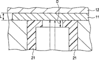
Figure 1B is the zoomed-in view of the part with laser beam irradiation shown in the cross section IB of Figure 1A.For by with KrF excimer laser beam (wavelength: 248nm) or the four-time harmonic of YAG laser beam (wavelength: 266nm) process Parylene opening 30 will be formed with high accuracy, and in order to make the Al-Si layer 11 that serves as wiring layer act on the wiring to energy generating element by electric power transfer by fully stoping laser beam and using satisfactorily, below meeting: the thickness D of parylene film 21 is 0.5~5 μ m, and the thickness L of Al-Si layer 11 is 0.1~3 μ m.
Then, as shown in Figure 2 F, the metal film that serves as conducting film is formed on the back of the body surface of base material and the inner side of recess by vapour deposition, and, by patterning, form the through electrode 24 that serves as the second electrode lay.
Fig. 6 is the cross sectional view that schematically shows the head that is assembled with the ink jet print head base material with through electrode of manufacturing in the present embodiment.The base material forming as shown in Fig. 2 A~2F is cut into chip (chips), and described chip is installed on the chip board (chipplate) that is provided with wiring and conductive welding disk, has then been sealed the manufacture of described head.
The second embodiment
As another example, below will describe according to the manufacture method of the ink jet print head base material with through electrode of the second embodiment.To the factor different from the first embodiment mainly be described.
The second embodiment is such example, and wherein, the wiring layer 11 that serves as drive circuit wiring is formed on heat oxide film 13, and has the structure that realizes the element separation in semiconductor devices by heat oxide film 13.
As shown in Figure 3 B, by the deposition growing such as hot CVD, the heat oxide film 13 that serves as insulating barrier is formed on silicon substrate 2.Incidentally, in actual CVD step, heat oxide film is formed in each in two surfaces of silicon substrate.Yet, for simplified characterization, by the heat oxide film of only describing on the front surface of base material.
Before forming heat oxide film, as shown in Figure 3 B, the part that forms through electrode can be covered with the nitride film of silicon etc., to prevent the growth of heat oxide film.
Because heat oxide film is grown in being used to form a plurality of heating stepses of semiconductor element, as shown in Figure 3 C, etching heat oxide film before forming wiring layer just, to expose the surface of silicon substrate completely.
Then, as shown in Figure 3 D, form the wiring layer that serves as drive circuit wiring.Forming energy producing component 1 as in the first embodiment.
Then, as shown in Figure 4 A, form inorganic protective film 12.Can form as in the first embodiment inorganic protective film 12.
Then, as shown in Figure 4 B, by coating outlet, form parts 3, form as in the first embodiment black outlet 4.
Then, as shown in Figure 4 C, by the Deep-RIE method such as Bosch technique, from the back of the body face side of silicon substrate 2, form recess 5.
In this case, selective due to etching gas, thereby heat oxide film is not etched, thus recess 5 has the shape shown in Fig. 4 C.
Then, as shown in Figure 5A, in order to ensure the required resistance to black characteristic of through electrode, by organic C VD, on the whole back of the body surface of base material, form protectiveness resin molding 21.
In the present embodiment, recess has complicated bottom shape as shown in Figure 5A.
Then, as shown in Figure 5 B, as in the first embodiment, utilize laser selective and remove the protectiveness resin molding 23 of concave bottom.
Then, as shown in Figure 5 C, by vapour deposition, form the metal film that serves as conducting film, and, by patterning, in the inner side of base material, form through electrode 24.
The base material forming as shown in Fig. 3 A~5C is cut into chip, and described chip is installed on the chip board that is provided with wiring and conductive welding disk, has then been sealed the manufacture of described head.
Although described the present invention with reference to exemplary embodiment, should be understood that and the invention is not restricted to disclosed exemplary embodiment.The scope of following claim should be endowed the 26S Proteasome Structure and Function of the widest explanation to comprise all such alter modes and to be equal to.
Claims (10)
1. a method of manufacturing liquid discharge head base material, comprising:
Prepare base material, described base material has first surface, and described first surface is provided with and produces for discharging the element of energy of liquid and the electrode layer being electrically connected to described element;
On second surface, form recess, described second surface is the surface of the opposition side of described first surface, and wherein, a part for electrode layer is served as the bottom surface of described recess;
With dielectric film, cover inside face and the bottom surface of described recess;
By utilizing laser to remove a part for the described bottom surface of covering of dielectric film, partly expose described electrode layer; And
Formation extends through the electrode of second surface from the first surface of base material, so that described electrode is electrically connected to the exposed portions serve of described electrode layer.
2. method according to claim 1, wherein, described electrode layer laser resistant intensity is greater than to this intensity of described dielectric film.
3. method according to claim 1, wherein, described laser is to be 1 μ s or shorter pulse laser beam in the pulse duration.
4. method according to claim 1, wherein, described laser is the short light of the visible light wavelength of wavelength ratio.
5. method according to claim 1, wherein, described dielectric film is made by any material of selecting from epoxy resin, polyimides, polyamide, polyureas and Parylene.
6. method according to claim 1, wherein, described electrode layer is made by contain at least one the metal of selecting from aluminium, copper and gold.
7. method according to claim 1, wherein, described electrode layer is made by the alloy of aluminium and silicon; Described dielectric film is made by Parylene; Described laser is by using the excimer laser beam being produced by krypton and fluorine gas to obtain.
8. method according to claim 1, wherein, described electrode layer is made by the alloy of aluminium and silicon; Described dielectric film is made by Parylene; Described laser contains the light that the wavelength being produced by Yttrium-Aluminium-Garnet is about 266nm.
9. method according to claim 7, wherein, the dielectric film of being made by Parylene has the thickness of 0.5 μ m~5 μ m; Described electrode layer has the thickness of 0.1 μ m~3 μ m.
10. method according to claim 8, wherein, the dielectric film of being made by Parylene has the thickness of 0.5 μ m~5 μ m; Described electrode layer has the thickness of 0.1 μ m~3 μ m.
Applications Claiming Priority (2)
| Application Number | Priority Date | Filing Date | Title |
|---|---|---|---|
| JP2009-204640 | 2009-09-04 | ||
| JP2009204640 | 2009-09-04 |
Publications (2)
| Publication Number | Publication Date |
|---|---|
| CN102009527A CN102009527A (en) | 2011-04-13 |
| CN102009527B true CN102009527B (en) | 2014-03-19 |
Family
ID=43648097
Family Applications (1)
| Application Number | Title | Priority Date | Filing Date |
|---|---|---|---|
| CN201010269391.9A Expired - Fee Related CN102009527B (en) | 2009-09-04 | 2010-08-31 | Process of producing liquid discharge head base material |
Country Status (4)
| Country | Link |
|---|---|
| US (1) | US8445298B2 (en) |
| JP (1) | JP5606213B2 (en) |
| KR (1) | KR101435239B1 (en) |
| CN (1) | CN102009527B (en) |
Families Citing this family (9)
| Publication number | Priority date | Publication date | Assignee | Title |
|---|---|---|---|---|
| JP5701014B2 (en) * | 2010-11-05 | 2015-04-15 | キヤノン株式会社 | Method for manufacturing ejection element substrate |
| JP5769560B2 (en) * | 2011-09-09 | 2015-08-26 | キヤノン株式会社 | Substrate for liquid discharge head and manufacturing method thereof |
| US10035346B2 (en) | 2015-01-27 | 2018-07-31 | Canon Kabushiki Kaisha | Element substrate and liquid ejection head |
| JP6598658B2 (en) * | 2015-01-27 | 2019-10-30 | キヤノン株式会社 | Element substrate for liquid discharge head and liquid discharge head |
| EP3231007B1 (en) * | 2015-01-30 | 2021-04-14 | Hewlett-Packard Development Company, L.P. | Atomic layer deposition passivation for via |
| JP6881967B2 (en) * | 2016-12-22 | 2021-06-02 | キヤノン株式会社 | Substrate manufacturing method |
| JP7224782B2 (en) * | 2018-05-30 | 2023-02-20 | キヤノン株式会社 | Liquid ejection head and manufacturing method thereof |
| JP7237480B2 (en) * | 2018-06-29 | 2023-03-13 | キヤノン株式会社 | Liquid ejection head and manufacturing method thereof |
| US11161351B2 (en) * | 2018-09-28 | 2021-11-02 | Canon Kabushiki Kaisha | Liquid ejection head |
Citations (2)
| Publication number | Priority date | Publication date | Assignee | Title |
|---|---|---|---|---|
| US5694684A (en) * | 1994-06-10 | 1997-12-09 | Canon Kabushiki Kaisha | Manufacturing method for ink jet recording head |
| CN1976811A (en) * | 2004-06-28 | 2007-06-06 | 佳能株式会社 | Manufacturing method for liquid ejecting head and liquid ejecting head obtained by this method |
Family Cites Families (5)
| Publication number | Priority date | Publication date | Assignee | Title |
|---|---|---|---|---|
| JPH05147223A (en) * | 1991-12-02 | 1993-06-15 | Matsushita Electric Ind Co Ltd | Ink jet head |
| JPH06312509A (en) | 1993-04-30 | 1994-11-08 | Canon Inc | Ink jet record head, manufacture thereof, and ink jet recording device equipped therewith |
| JPH09314607A (en) * | 1996-05-24 | 1997-12-09 | Ricoh Co Ltd | Method for adjusting injection mold, film for adjusting mold and its production |
| US6790775B2 (en) * | 2002-10-31 | 2004-09-14 | Hewlett-Packard Development Company, L.P. | Method of forming a through-substrate interconnect |
| US7926909B2 (en) * | 2007-01-09 | 2011-04-19 | Canon Kabushiki Kaisha | Ink-jet recording head, method for manufacturing ink-jet recording head, and semiconductor device |
-
2010
- 2010-08-18 JP JP2010183153A patent/JP5606213B2/en active Active
- 2010-08-27 KR KR1020100083346A patent/KR101435239B1/en active IP Right Grant
- 2010-08-30 US US12/871,233 patent/US8445298B2/en not_active Expired - Fee Related
- 2010-08-31 CN CN201010269391.9A patent/CN102009527B/en not_active Expired - Fee Related
Patent Citations (2)
| Publication number | Priority date | Publication date | Assignee | Title |
|---|---|---|---|---|
| US5694684A (en) * | 1994-06-10 | 1997-12-09 | Canon Kabushiki Kaisha | Manufacturing method for ink jet recording head |
| CN1976811A (en) * | 2004-06-28 | 2007-06-06 | 佳能株式会社 | Manufacturing method for liquid ejecting head and liquid ejecting head obtained by this method |
Non-Patent Citations (1)
| Title |
|---|
| JP特开平6-312509A 1994.11.08 |
Also Published As
| Publication number | Publication date |
|---|---|
| CN102009527A (en) | 2011-04-13 |
| KR101435239B1 (en) | 2014-08-28 |
| KR20110025605A (en) | 2011-03-10 |
| US8445298B2 (en) | 2013-05-21 |
| US20110059558A1 (en) | 2011-03-10 |
| JP2011073440A (en) | 2011-04-14 |
| JP5606213B2 (en) | 2014-10-15 |
Similar Documents
| Publication | Publication Date | Title |
|---|---|---|
| CN102009527B (en) | Process of producing liquid discharge head base material | |
| US5733433A (en) | Heat generating type ink-jet print head | |
| JP5767359B2 (en) | Manufacturing method of solar cell | |
| KR100459905B1 (en) | Monolithic inkjet printhead having heater disposed between dual ink chamber and method of manufacturing thereof | |
| CN102576767B (en) | Metal grid contact pattern and dielectric pattern are formed into the method needed on the solar cell layer of conductive contact | |
| US7475966B2 (en) | Liquid discharge recording head and method for manufacturing same | |
| JPS61230954A (en) | Manufacture of printing head for heat-sensitive ink jet | |
| JP2011073440A5 (en) | ||
| US7104632B2 (en) | Monolithic ink-jet printhead and method for manufacturing the same | |
| KR100493160B1 (en) | Monolithic ink jet printhead having taper shaped nozzle and method of manufacturing thereof | |
| KR100560593B1 (en) | Method for manufacturing liquid ejection head | |
| JP2004358971A (en) | Integral-type inkjet print head and manufacturing method therefor | |
| US4835553A (en) | Thermal ink jet printhead with increased drop generation rate | |
| US7757397B2 (en) | Method for forming an element substrate | |
| US8012773B2 (en) | Method for manufacturing liquid discharge head | |
| KR100552664B1 (en) | Monolithic ink jet printhead having ink chamber defined by side wall and method of manufacturing thereof | |
| KR20040035910A (en) | Monolithic ink jet printhead with metal nozzle plate and method of manufacturing thereof | |
| JP2004351931A (en) | Ink-jet printhead and its manufacturing method | |
| KR101064043B1 (en) | Method for forming a connection between an electrode and an actuator in an inkjet nozzle assembly | |
| CN1883945A (en) | Inkjet printer head and fabrication method thereof | |
| KR20050056000A (en) | Monolithic inkjet printhead having two pairs of heaters and manufacturing method thereof | |
| KR20050001792A (en) | Monolithic inkjet printhead having auxiliary heater |
Legal Events
| Date | Code | Title | Description |
|---|---|---|---|
| C06 | Publication | ||
| PB01 | Publication | ||
| C10 | Entry into substantive examination | ||
| SE01 | Entry into force of request for substantive examination | ||
| GR01 | Patent grant | ||
| GR01 | Patent grant | ||
| CF01 | Termination of patent right due to non-payment of annual fee |
Granted publication date: 20140319 Termination date: 20210831 |
|
| CF01 | Termination of patent right due to non-payment of annual fee |