CN101867003B - Light emitting device - Google Patents
Light emitting device Download PDFInfo
- Publication number
- CN101867003B CN101867003B CN2010101674925A CN201010167492A CN101867003B CN 101867003 B CN101867003 B CN 101867003B CN 2010101674925 A CN2010101674925 A CN 2010101674925A CN 201010167492 A CN201010167492 A CN 201010167492A CN 101867003 B CN101867003 B CN 101867003B
- Authority
- CN
- China
- Prior art keywords
- light
- mentioned
- transparent member
- emitting device
- emitting component
- Prior art date
- Legal status (The legal status is an assumption and is not a legal conclusion. Google has not performed a legal analysis and makes no representation as to the accuracy of the status listed.)
- Active
Links
Images


Classifications
-
- H—ELECTRICITY
- H01—ELECTRIC ELEMENTS
- H01L—SEMICONDUCTOR DEVICES NOT COVERED BY CLASS H10
- H01L33/00—Semiconductor devices with at least one potential-jump barrier or surface barrier specially adapted for light emission; Processes or apparatus specially adapted for the manufacture or treatment thereof or of parts thereof; Details thereof
- H01L33/48—Semiconductor devices with at least one potential-jump barrier or surface barrier specially adapted for light emission; Processes or apparatus specially adapted for the manufacture or treatment thereof or of parts thereof; Details thereof characterised by the semiconductor body packages
- H01L33/50—Wavelength conversion elements
-
- H—ELECTRICITY
- H01—ELECTRIC ELEMENTS
- H01L—SEMICONDUCTOR DEVICES NOT COVERED BY CLASS H10
- H01L33/00—Semiconductor devices with at least one potential-jump barrier or surface barrier specially adapted for light emission; Processes or apparatus specially adapted for the manufacture or treatment thereof or of parts thereof; Details thereof
- H01L33/48—Semiconductor devices with at least one potential-jump barrier or surface barrier specially adapted for light emission; Processes or apparatus specially adapted for the manufacture or treatment thereof or of parts thereof; Details thereof characterised by the semiconductor body packages
- H01L33/58—Optical field-shaping elements
-
- H—ELECTRICITY
- H01—ELECTRIC ELEMENTS
- H01L—SEMICONDUCTOR DEVICES NOT COVERED BY CLASS H10
- H01L33/00—Semiconductor devices with at least one potential-jump barrier or surface barrier specially adapted for light emission; Processes or apparatus specially adapted for the manufacture or treatment thereof or of parts thereof; Details thereof
- H01L33/48—Semiconductor devices with at least one potential-jump barrier or surface barrier specially adapted for light emission; Processes or apparatus specially adapted for the manufacture or treatment thereof or of parts thereof; Details thereof characterised by the semiconductor body packages
- H01L33/64—Heat extraction or cooling elements
-
- H—ELECTRICITY
- H01—ELECTRIC ELEMENTS
- H01L—SEMICONDUCTOR DEVICES NOT COVERED BY CLASS H10
- H01L2224/00—Indexing scheme for arrangements for connecting or disconnecting semiconductor or solid-state bodies and methods related thereto as covered by H01L24/00
- H01L2224/01—Means for bonding being attached to, or being formed on, the surface to be connected, e.g. chip-to-package, die-attach, "first-level" interconnects; Manufacturing methods related thereto
- H01L2224/02—Bonding areas; Manufacturing methods related thereto
- H01L2224/04—Structure, shape, material or disposition of the bonding areas prior to the connecting process
- H01L2224/05—Structure, shape, material or disposition of the bonding areas prior to the connecting process of an individual bonding area
- H01L2224/0554—External layer
- H01L2224/0556—Disposition
- H01L2224/05568—Disposition the whole external layer protruding from the surface
-
- H—ELECTRICITY
- H01—ELECTRIC ELEMENTS
- H01L—SEMICONDUCTOR DEVICES NOT COVERED BY CLASS H10
- H01L2224/00—Indexing scheme for arrangements for connecting or disconnecting semiconductor or solid-state bodies and methods related thereto as covered by H01L24/00
- H01L2224/01—Means for bonding being attached to, or being formed on, the surface to be connected, e.g. chip-to-package, die-attach, "first-level" interconnects; Manufacturing methods related thereto
- H01L2224/02—Bonding areas; Manufacturing methods related thereto
- H01L2224/04—Structure, shape, material or disposition of the bonding areas prior to the connecting process
- H01L2224/05—Structure, shape, material or disposition of the bonding areas prior to the connecting process of an individual bonding area
- H01L2224/0554—External layer
- H01L2224/05573—Single external layer
-
- H—ELECTRICITY
- H01—ELECTRIC ELEMENTS
- H01L—SEMICONDUCTOR DEVICES NOT COVERED BY CLASS H10
- H01L2224/00—Indexing scheme for arrangements for connecting or disconnecting semiconductor or solid-state bodies and methods related thereto as covered by H01L24/00
- H01L2224/01—Means for bonding being attached to, or being formed on, the surface to be connected, e.g. chip-to-package, die-attach, "first-level" interconnects; Manufacturing methods related thereto
- H01L2224/10—Bump connectors; Manufacturing methods related thereto
- H01L2224/12—Structure, shape, material or disposition of the bump connectors prior to the connecting process
- H01L2224/14—Structure, shape, material or disposition of the bump connectors prior to the connecting process of a plurality of bump connectors
-
- H—ELECTRICITY
- H01—ELECTRIC ELEMENTS
- H01L—SEMICONDUCTOR DEVICES NOT COVERED BY CLASS H10
- H01L2224/00—Indexing scheme for arrangements for connecting or disconnecting semiconductor or solid-state bodies and methods related thereto as covered by H01L24/00
- H01L2224/01—Means for bonding being attached to, or being formed on, the surface to be connected, e.g. chip-to-package, die-attach, "first-level" interconnects; Manufacturing methods related thereto
- H01L2224/10—Bump connectors; Manufacturing methods related thereto
- H01L2224/15—Structure, shape, material or disposition of the bump connectors after the connecting process
- H01L2224/16—Structure, shape, material or disposition of the bump connectors after the connecting process of an individual bump connector
- H01L2224/161—Disposition
- H01L2224/16151—Disposition the bump connector connecting between a semiconductor or solid-state body and an item not being a semiconductor or solid-state body, e.g. chip-to-substrate, chip-to-passive
- H01L2224/16221—Disposition the bump connector connecting between a semiconductor or solid-state body and an item not being a semiconductor or solid-state body, e.g. chip-to-substrate, chip-to-passive the body and the item being stacked
- H01L2224/16225—Disposition the bump connector connecting between a semiconductor or solid-state body and an item not being a semiconductor or solid-state body, e.g. chip-to-substrate, chip-to-passive the body and the item being stacked the item being non-metallic, e.g. insulating substrate with or without metallisation
-
- H—ELECTRICITY
- H01—ELECTRIC ELEMENTS
- H01L—SEMICONDUCTOR DEVICES NOT COVERED BY CLASS H10
- H01L2924/00—Indexing scheme for arrangements or methods for connecting or disconnecting semiconductor or solid-state bodies as covered by H01L24/00
- H01L2924/0001—Technical content checked by a classifier
- H01L2924/00014—Technical content checked by a classifier the subject-matter covered by the group, the symbol of which is combined with the symbol of this group, being disclosed without further technical details
-
- H—ELECTRICITY
- H01—ELECTRIC ELEMENTS
- H01L—SEMICONDUCTOR DEVICES NOT COVERED BY CLASS H10
- H01L33/00—Semiconductor devices with at least one potential-jump barrier or surface barrier specially adapted for light emission; Processes or apparatus specially adapted for the manufacture or treatment thereof or of parts thereof; Details thereof
- H01L33/44—Semiconductor devices with at least one potential-jump barrier or surface barrier specially adapted for light emission; Processes or apparatus specially adapted for the manufacture or treatment thereof or of parts thereof; Details thereof characterised by the coatings, e.g. passivation layer or anti-reflective coating
- H01L33/46—Reflective coating, e.g. dielectric Bragg reflector
-
- H—ELECTRICITY
- H01—ELECTRIC ELEMENTS
- H01L—SEMICONDUCTOR DEVICES NOT COVERED BY CLASS H10
- H01L33/00—Semiconductor devices with at least one potential-jump barrier or surface barrier specially adapted for light emission; Processes or apparatus specially adapted for the manufacture or treatment thereof or of parts thereof; Details thereof
- H01L33/48—Semiconductor devices with at least one potential-jump barrier or surface barrier specially adapted for light emission; Processes or apparatus specially adapted for the manufacture or treatment thereof or of parts thereof; Details thereof characterised by the semiconductor body packages
- H01L33/50—Wavelength conversion elements
- H01L33/505—Wavelength conversion elements characterised by the shape, e.g. plate or foil
-
- H—ELECTRICITY
- H01—ELECTRIC ELEMENTS
- H01L—SEMICONDUCTOR DEVICES NOT COVERED BY CLASS H10
- H01L33/00—Semiconductor devices with at least one potential-jump barrier or surface barrier specially adapted for light emission; Processes or apparatus specially adapted for the manufacture or treatment thereof or of parts thereof; Details thereof
- H01L33/48—Semiconductor devices with at least one potential-jump barrier or surface barrier specially adapted for light emission; Processes or apparatus specially adapted for the manufacture or treatment thereof or of parts thereof; Details thereof characterised by the semiconductor body packages
- H01L33/58—Optical field-shaping elements
- H01L33/60—Reflective elements
Abstract
The light emitting device 100 has a light emitting element 101, and translucent material 102 that passes incident light from the light emitting element 101 and emits that light to the outside. The sides of the translucent material 102 perimeter are inclined surfaces 107 that become wider from the upper surface to the lower surface. The area of the lower surface of the translucent material 102 is formed larger than the area of the upper surface of the light emitting element 101. The lower surface of the translucent material 102 and the upper surface of the light emitting element 101 are joined together, and the part of the lower surface of the translucent material 102 that is not joined with the light emitting element 101 and the inclined surfaces 101 are covered by light reflecting resin 103.
Description
Technical field
The present invention relates to a kind of light-emitting device that possesses the light transmission department spare of the light that can transmission comes self-emission device.
Background technology
Semiconductor light-emitting elements can send brightly painted light, and the semiconductor light-emitting elements volume is little and power utilization efficient high.In addition, there is not the danger of bulb explosion etc. as the semiconductor light-emitting elements of semiconductor element.In addition, also have initial stage drive characteristic excellence, vibration resistance, be good at the feature of extinguishing of lighting repeatedly.In addition, developed such light-emitting device: the light source light that penetrates from semiconductor light-emitting elements by combination can penetrate the light wavelength transform component from the different form and aspect of light source light with being excited by this light source light, utilize the principle of light colour mixture, can penetrate the light-emitting device of the light of various color.Because have the characteristic of such excellence, the semiconductor light-emitting elements of light-emitting diode (Light Emitting Diode:LED), laser diode (Laser Diode:LD) etc. is utilized as various light sources.Particularly in recent years, as the illuminating light source of having fetched fluorescent lamp, as more low power consumption, more long-life time from generation to generation illumination and extensively attracted attention, therefore also wish further to improve luminous output, improve luminous efficiency.In addition, also wish to obtain flood light, the directive property excellence the floodlighting (floodlight) and the light source of high brightness such as the headlight of car etc.
As such light-emitting device, for example in TOHKEMY 2007-19096 communique patent documentation 1, put down in writing light-emitting device 900, the cutaway view of this light-emitting device 900 is as shown in figure 10.Light-emitting device 900 comprises LED element 901 and carries the housing 904 of this LED element 901.Housing 904 has opening in light emission (light emitting gets り and goes out) side, is placed with LED element 901 in open interior.In addition, in housing 904, be filled with coating (coating) material 903 that contains the light reflective particle, the zone, outside except light emitting surface of LED element 901 is covered by this coating material 903.
And, on the outside of the coating material 903 that is shaped and also be provided with the luminescent coating 902 of sheet at light emitting surface.Yttrium-aluminium-garnet) etc. luminescent coating 902 is by comprising that (Yttrium Aluminum Gamet: the resin of fluorophor consists of YAG, this fluorophor receives from the radiating light (blue light) of LED element 901 and is excited, and radiation wavelength conversion light (sodium yellow).
In addition, luminescent coating 902 constitutes the whole light emitting surface that covers LED element 901, and has the light-emitting area that is exposed to the light emitting side.Thus, come the once light (blue light) of word LED element 901 and this once the part of the light secondary light (sodium yellow) after by wavelength conversion carry out colour mixture, obtain white light from light-emitting area.
Yet, for above-mentioned such light-emitting device, when the thermal history (thermal history) when making or the temperature when using rise each component parts generation thermal deformation of light-emitting device, luminescent coating 902 is positioned at the upwards pushing of coating material 903 below it, the problem of peeling off, coming off can occur.In addition, because slighter to the heat dissipation capacity the atmosphere from the light-emitting area of luminescent coating 902, although therefore need to increase as heat to pass on the coating material 903 of route and the contact area of luminescent coating 902, if also become greatly but increase 902 light-emitting areas of luminescent coating, thereby can cause the low problem of brightness.
Summary of the invention
Therefore the object of the invention be to provide a kind of can high brightness ground luminous and light-emitting device with reliability of excellence.
In order to reach above-mentioned purpose, light-emitting device of the present invention possesses: light-emitting component, with upper surface as light emitting surface; Transparent member has upper surface and lower surface, the lower surface incident from the light of above-mentioned light-emitting component outgoing from this transparent member, and penetrate to the outside via the upper surface of this transparent member; And the light reflective resin, cover at least a portion of above-mentioned transparent member.The circumferential lateral surface of above-mentioned transparent member has from the upper surface direction towards the inclined plane lower surface Directional Extension, that join with lower surface, the area of the lower surface of above-mentioned transparent member forms larger than the area of the upper surface of above-mentioned light-emitting component, the lower surface of above-mentioned transparent member and the upper surface of above-mentioned light-emitting component engage, and the part and the above-mentioned inclined plane that do not engage with above-mentioned light-emitting component in the lower surface of above-mentioned transparent member are covered by above-mentioned light reflective resin.Thus, the light-emitting device luminous, that have excellent reliability that realization can high brightness.
In addition, the circumferential lateral surface of above-mentioned transparent member can all form the inclined plane.
The circumferential lateral surface of above-mentioned transparent member can begin until the centre of circumferential lateral surface forms vertical guide from upper surface, from this centre beginning until lower surface forms above-mentioned inclined plane.
In addition, it is respectively the general planar face that the upper surface of above-mentioned transparent member and lower surface can form, and mutual almost parallel.
In addition, the upper surface of above-mentioned transparent member can form and above-mentioned light reflective resin same plane roughly.
In addition, above-mentioned inclined plane can be the general planar face.
The lower surface that in addition, can constitute above-mentioned transparent member has: the composition surface that engages with the upper surface of above-mentioned light-emitting component; And expose from above-mentioned composition surface expose face, above-mentioned transparent member expose face and above-mentioned inclined plane angulation θ 2 is acute angles, the upper surface of above-mentioned transparent member and above-mentioned inclined plane angulation θ 1 are the obtuse angle.
In addition, the above-mentioned area that exposes face can be 10%~100% of described composition surface with respect to the composition surface.
In addition, light-emitting device can also possess substrate, and this substrate is used for placing above-mentioned light-emitting component and light reflective resin.
In addition, above-mentioned transparent member can constitute and contain fluorophor.
In addition, the side of above-mentioned light-emitting component can be covered by above-mentioned light reflective resin.
Perhaps, above-mentioned light-emitting component can be provided with pair of electrodes at the lower surface relative with its upper surface.
In addition, above-mentioned inclined plane can account for circumferential lateral surface about more than 50% of above-mentioned transparent member.
Another kind of light-emitting device possesses: light-emitting component, with upper surface as light emitting surface; Transparent member has upper surface and lower surface, the lower surface incident from the light of above-mentioned light-emitting component outgoing from this transparent member, and penetrate to the outside via the upper surface of this transparent member; And the light reflective resin, cover at least a portion of above-mentioned transparent member.At this, the circumferential lateral surface of above-mentioned transparent member begins until the centre of circumferential lateral surface forms the inclined plane from upper surface, from this centre beginning until lower surface forms vertical guide, the lower surface of above-mentioned transparent member and the upper surface of above-mentioned light-emitting component engage, and the part and the above-mentioned inclined plane that do not engage with above-mentioned light-emitting component in the lower surface of above-mentioned transparent member are covered by above-mentioned light reflective resin.
Another kind of light-emitting device possesses: light-emitting component, with upper surface as light emitting surface; Transparent member has upper surface and lower surface, the lower surface incident from the light of above-mentioned light-emitting component outgoing from this transparent member, and penetrate to the outside via the upper surface of this transparent member; And light reflective resin, cover at least a portion of above-mentioned transparent member, the circumferential lateral surface of above-mentioned transparent member begins until the centre of circumferential lateral surface forms the inclined plane from upper surface, begin until lower surface forms to the anti-obliquity face of the direction inclination opposite with above-mentioned inclined plane from this centre, the lower surface of above-mentioned transparent member and the upper surface of above-mentioned light-emitting component engage, and the part and the above-mentioned inclined plane that do not engage with above-mentioned light-emitting component in the lower surface of above-mentioned transparent member are covered by above-mentioned light reflective resin.
In addition, above-mentioned inclined plane and above-mentioned anti-obliquity face angulation can be acute angle.
By the following detailed description also by reference to the accompanying drawings, can be to foregoing of the present invention with further material object and characteristics thereof be clearer.
Description of drawings
Fig. 1 is the general profile chart of the light-emitting device of expression embodiments of the present invention 1.
Fig. 2 is the general profile chart of the light-emitting device of expression embodiments of the present invention 2.
Fig. 3 is the general profile chart of the light-emitting device of expression embodiments of the present invention 3.
Fig. 4 is the general profile chart of the light-emitting device of expression embodiments of the present invention 4.
Fig. 5 is the general profile chart of the light-emitting device of expression embodiments of the present invention 5.
Fig. 6 is the figure of manufacture method of the transparent member of expression embodiments of the present invention 1.
Fig. 7 is the figure of manufacture method of the transparent member of expression embodiments of the present invention 2.
Fig. 8 is the figure of manufacture method of the transparent member of expression embodiments of the present invention 3.
Fig. 9 is the figure of manufacture method of the transparent member of expression embodiments of the present invention 4.
Figure 10 is the general profile chart that represents light-emitting device in the past.
Symbol description
100,200,300,400,500,900 light-emitting devices
101 light-emitting components
102 transparent members
103 light reflective resins
104 substrates
105 conductive components
The 106a junction surface
The 106b exposed division
107 inclined planes
108 upper surfaces
109 sides
110 anti-obliquity faces
111 vertical planes
Cutter is used in 112 oblique angles cuttings (bevel cut)
Embodiment
Below, with reference to the accompanying drawings embodiments of the present invention are described.
<execution mode 1 〉
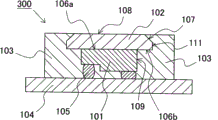
Fig. 1 is the general profile chart of the light-emitting device 100 of expression present embodiment 1.Light-emitting device 100 shown in Figure 1 possesses light-emitting component 101, transmission is from the light of light-emitting component 101 outgoing and the transparent member 102 that penetrates to the outside, the circumferential lateral surface of transparent member 102 has the inclined plane 107 of the expansion (Wide Ga Ru) from upper surface to lower surface, the area of the lower surface of transparent member 102 forms larger than the area of the upper surface of light-emitting component 101, the upper surface of the lower surface of transparent member 102 and light-emitting component 101 engages, being covered with by light reflective resin 103 with light-emitting component 101 asynthetic parts and inclined plane 107 in the lower surface of transparent member 102.Lower surface describes each parts and the structure of light-emitting device 100 of the present invention.
(light-emitting component 101)
Employed light-emitting component 101 is not particularly limited in this among the present invention, can utilize known element, in the present invention, and as the light-emitting component 101 preferred light-emitting diodes that use.
Light-emitting component can be selected the element of any wavelength.For example, the light-emitting component as blue, green can use ZnSe, nitride semiconductor (In
xAl
YGa
1-X-YN, 0≤X, 0≤Y, X+Y≤1), the element of GaP.In addition, as the light-emitting component of redness, can use GaAlAs, AlInGaP etc.In addition, also can use the semiconductor light-emitting elements that is consisted of by in addition material.The composition of employed light-emitting component, illuminant colour, size, number etc. can suitably be selected according to purpose.
Have in employing in the situation of light-emitting device of fluorophor, preferably send the efficiently nitride-based semiconductor (In of the short wavelength's of excited fluophor light
xAl
YGa
1-X-YN, 0≤X, 0≤Y, X+Y≤1).Can select multiple emission wavelength according to material, the mixed crystal degree of semiconductor layer.
The light-emitting component 101 of present embodiment 1 is to have positive and negative pair of electrodes in the same face side, pair of electrodes via conductive component 105 by the upside-down mounting chip be installed on the conductor wiring (not shown) of substrate 104, face that will be relative with the face that has formed electrode is as light emitting surface.Light-emitting component 101 be growth in light transmission with Sapphire Substrate on lamination nitride-based semiconductor and the light-emitting component that forms, Sapphire Substrate becomes the upper surface side of light-emitting component 101, becomes light emitting surface.Sapphire Substrate has concavo-convex on the composition surface with nitride semiconductor layer, can change thus the critical angle when running into Sapphire Substrate from the light of nitride semiconductor layer outgoing intentionally, and light is launched from the outside of Sapphire Substrate easily.Laser lift-off) etc. in addition, also can removing grows up use substrate, such as (Laser LiftOff: method is removed by grinding, LLO.In addition, such growth also is not limited to Sapphire Substrate with substrate, can suitably change.
(transparent member 102)
As can send with the blue light emitting device appropriate combination white light, employed representational fluorophor in the wavelength conversion parts, for example, fluorophor that preferably use YAG (Yttrium Aluminum Garnet) to be, BOS (Barium ortho-Silicate) is etc. etc.In the situation of the light-emitting device that can send white light, the mode that becomes white with the concentration of utilizing the fluorophor that contains in the transparent member 102 is adjusted.The concentration of fluorophor can suitably change, for example, and about 5%~50%.Since some its light emission effciencies of thin thickness of transparent member 102 well therefore should be preferably thin transparent member 102, but because thinner then intensity is lower, therefore preferred suitably adjustment in the preferable range of above-mentioned phosphor concentration and thickness.
In addition, by contain red-emitting phosphors in the engagement member that engages transparent member 102 and blue light emitting device, can become the light-emitting device according to the light of the electric ball look of sending of JIS specification, wherein said joint transparent member 102 contains the wavelength conversion parts.That is, by the blue light that sends from light-emitting component 101 with from the sodium yellow of fluorophor~red light colour mixture, thereby send the white light of warm colour system.From beginning to dispose the fluorophor from the long wave to the shortwave near the light-emitting component 101, so the light emission effciency is good, by in the near engagement member of distance light-emitting component, containing red-emitting phosphors, thus utilizing emitted light efficiently.Since be configured in light-emitting component 101 near, therefore preferred heat-resisting fluorophor.
By the lower surface at transparent member 102 form concavo-convex, can make the incident light scattering of self-emission device 101, thereby it is uneven easily to reduce brightness disproportionation, form and aspect.Particularly in 1 transparent member 102 and situation that a plurality of light-emitting components 101 engage, the impact of the impact of the configuration of each light-emitting component 102, consequent luminous intensity distribution, brightness disproportionation, form and aspect inequality is large, therefore preferably can reduce the structure of these impacts.
(joint of light-emitting component 101 and transparent member 102)
For example as shown in Figure 1, the lower surface of the upper surface of the light-emitting component that becomes light emitting surface 101 of light-emitting component 101 and transparent member 102 engages at composition surface 106a place.Joint can be for example pressing, sintering, utilize the such known bonding agent of epoxy resin or silicon bonding, the organic adhesive that utilizes high index of refraction bonding, utilize the bonding etc. of low melting point glass.In addition, here " joint " not only refers to direct joint, also comprises the joint that utilizes bonding agent, miscellaneous part and carry out.At this, the area of the lower surface of transparent member 102 forms larger than the area of the upper surface of light-emitting component 101.Thus, transparent member 102 utilizes the face larger than the light-emitting face of light-emitting component 101 to be subjected to light, thereby can reduce the loss of light.In addition, transparent member 102 is configured in light-emitting component 101 above the time, even produce position deviation to a certain degree, the upper surface of light-emitting component is all covered by the lower surface 106 of transparent member, the variation of the brightness that therefore produces because of installation deviation exists hardly, can enhance productivity.What is called herein " area ", when the upper surface of the lower surface of transparent member 102 and light-emitting component 101 is tabular surface, then refer to surface area, in the situation that is not tabular surface, the area of the part that then refers to see from the upper surface side of transparent member 102, transparent member 102 and light-emitting component 101 are overlapping.That is, from upper surface 108 sides of transparent member, the size of the upper surface of light-emitting component 101 forms by transparent member 102 interior bags, and the upper surface of light-emitting component 101 is covered with by transparent member 102.If form like this, then transparent member 102 have in its lower surface with the asynthetic part of above-mentioned light-emitting component, in other words, the part that the composition surface 106a that engages from the lower surface of the upper surface of light-emitting component 101 and transparent member 102 exposes (below, be also referred to as and expose face 106b).The area that exposes face 106b is 10%~100% with respect to composition surface 106a.
Exposing in the situation that face 106b and inclined plane 107 link, as shown in Figure 1, transparent member 102 expose face 106b and inclined plane described later 107 angulation θ
2Be acute angle, become in the outstanding shape of composition surface side outward direction.Thus, even when the light emitting element 101 and the light-transmissive member 102 is in engagement with the engaging member, it is possible by having an exposed surface 106b to suppress the inclined surface of the engaging member 107 toward the upward creep (Kei on this bittern).Engagement member is owing to absorb or scattering comes the light of self-emission device, therefore in order to make light reflective resin 103 reflect efficiently the light that comes self-emission device 101, the attachment of engagement member etc. is not set on composition surface 106a face in addition preferably.But this does not hinder attachment to begin to extend to inclined plane 107 through exposing face 106b from composition surface 106a.In addition, expose the parts that face 106b also can be reflected light, such as coverings such as metal films.Thus, expose face 106b even attachment extend to, also exposing efficiently reverberation of face 106b.
(inclined plane 107)
As shown in Figure 1, the circumferential lateral surface of the transparent member among the present invention 102 has the inclined plane 107 of the expansion from upper surface to lower surface.Such inclined plane 107 and the above-mentioned face 106b that exposes are covered by light reflective resin 103, can utilize thus light reflective parts 103 to lock transparent member 102, do not worry that therefore transparent member 102 peels off or come off.
In addition, because the bonding area of transparent member 102 and light reflective resin 103 becomes large, therefore can improve the thermal diffusivity of transparent member 102.
In addition, in making transparent member 102, contain in the situation of fluorophor, because peeling off of transparent member 102, be positioned at from light-emitting component 101 and begin to change to the abundance of the upper fluorophor of the distance of light-emitting face, produce sometimes colo(u)r bias (look ず れ), do not wish that this situation occurs.According to the present invention, transparent member 102 is locked by light reflective resin 103, so transparent member 102 can not peel off, and does not therefore worry producing colo(u)r bias.
Like this, by inclined plane 107 is set, form littlely so that transparent member 102 is exposed to outside part in upper surface 108 sides, make the part that embeds in the light reflective resin 103 form greatlyr, therefore at the thermal diffusivity that can not cause to improve under the low prerequisite of brightness transparent member 102, can reduce the thermal resistance of light-emitting device.Particularly, when in transparent member 102, containing fluorophor and the light that comes self-emission device being carried out wavelength conversion, fluorophor can cause self-heating because of energy loss (stokes loss), based on this heat the light conversion efficiency of fluorophor is reduced, therefore needs dispel the heat to the heat of fluorophor efficiently.Therefore, make in the transparent member 102 and contain fluorophor, make the contact area heat radiation route and light reflective resin 103 as transparent member 102 become large, thereby can improve the thermal diffusivity of transparent member 102 even fluorophor.By inclined plane 107 is set, situation about forming with the lower surface of the vertical upper surface 108 that is connected transparent member 102 and transparent member 102 is compared, and it is large that the area of side becomes, and can obtain larger and contact area light reflective resin 103.
At this, inclined plane 107 also can not link upper surface 108 and lower surface, as long as have the inclined plane 107 of the expansion from upper surface to lower surface at least a portion of its circumferential lateral surface.Therefore, the side of transparent member 102 also can have the different face that is different from inclined plane 107.In addition, larger than the above-mentioned area that exposes face 106b if the area on inclined plane 107 is set as, the effect that then locks is large, therefore preferred such structure.
The lower surface that engages with light-emitting component 101 of the transparent member 102 in the execution mode 1 and the upper surface 108 that becomes exiting surface form the tabular of general planar almost parallel, have the inclined plane 107 of the expansion from upper surface to lower surface in the side.In Fig. 1, in other words, the upper surface 108 angulation θ 1 that inclined plane 107 forms with smooth formation are the obtuse angle, expose face 106b and inclined plane 107 and are covered by light reflective resin 103 one.Thus, transparent member 102 is locked at above-below direction by light reflective resin 103, can prevent that transparent member 102 from peeling off or come off.In addition, owing to can increase the bonding area of transparent member 102 and light reflective resin 103, therefore can increase the area of the face that transmits to light reflective resin 103 from the heat of transparent member 102, can improve the thermal diffusivity of transparent member 102.
(light reflective resin 103)
Among the present invention, as shown in Figure 1, light reflective resin 103 covers the inclined plane 107 of transparent member 102 and exposes face 106b.The light emitting surface of light-emitting component 101 is exposed, so that become possibility to the light inlet of transparent member 102 from light reflective resin 103.Light reflective resin 103 is made of the parts of the light that can reflect self-emission device 101, and the interface between transparent member 102 and light reflective resin 103 makes the light of self-emission device 101 to reflex in the transparent member 102.Like this, light is in transparent member 102 interior propagation, and finally the upper surface 108 from transparent member 102 penetrates to the outside.
At this, the upper surface of preferred light reflectivity resin 103 is lower than the height of the upper surface 108 of transparent member 102.Light also diffusion on transverse direction from upper surface 108 outgoing of the transparent member 102 that becomes light-emitting face.The upper surface of light reflective resin 103 than the high situation of the height of the upper surface of transparent member 102 under, run into light reflective resin 103 and be reflected from the light of the upper surface outgoing of transparent member 102, can produce thus the inequality of luminous intensity distribution.Therefore, Yi Bian the side by making transparent member is covered by light reflective resin 103, make the height of light reflective resin 103 of the periphery that covers the side low on one side, can make the light of outgoing directly to external emission, therefore preferred such structure.
In addition, light reflective parts 103 not only cover transparent member 102 and expose face 106b, also the side of preferred covering luminous element 101.Emergent light from from light-emitting component 101 to side surface direction is reflexed in the light-emitting component by light reflective resin 103, thereby to the lower surface incident light of light transmission section 102.
Material as light reflective resin 103, can be silicones, modified silicone resin, epoxy resin, denaturation loop epoxy resins, allyl resin, in addition, also can be to make the material that contains reflective substance in more than one the resin of hybrid resin etc. that comprises at least in these resins and form.As the material of reflective substance, can use titanium oxide, silicon dioxide, titanium dioxide, zirconium dioxide, potassium titanate, aluminium oxide, aluminium nitride, boron nitride, mullite etc.Owing to contain concentration, density and reflection of light amount, transmission amount are different according to it, therefore can according to shape, the size of light-emitting device, adjust suitable concentration, density.For example, in the situation of smaller light-emitting device, need to make the wall thickness of the 1st light-reflecting components little, for the leakage of the light that is suppressed at this thinner wall section, preferably improve the concentration of reflective substance.On the other hand, in the manufacturing process of the coating of light reflective resin 103, shaping etc., if uprise in the situation that then has the difficulty on making in the concentration of reflective substance, can suitably adjust concentration.For example, the concentration that contains of preferred reflective substance is more than the 30wt%, and its wall thickness is more than the 20/ μ m.
In addition, if adopted the material that has in the lump reflectivity and thermal diffusivity, then can either possess reflecting properties, can improve thermal diffusivity again.As such material, can enumerate the high aluminium nitride of pyroconductivity or boron nitride.In addition, also can outside reflective substance, add the thermal diffusivity material in order to improve thermal diffusivity.The concentration that contains with respect to resin of preferred these heat sink materials for example is more than the 5wt%, thus, so that the pyroconductivity of light reflective resin 103 is more than the 3W/mK.In addition, the light reflective parts preferably have the material identical with the main material of substrate 104 described later, can access thus the light-emitting device of thermal stress.
The manufacturing process of light reflective resin 103 is not particularly limited, and for example, can adopt injection molding, castable, resin print process, transfer die (transfer mould) method, compression molding etc. to be shaped.
In addition, in light-emitting device of the present invention, also can carry the protection component of Zener diode etc.By these protection components are embedded in the light reflective resin 103, can prevent from blocking cause photoemissive low because of the absorption of light protected element or the protected element that come self-emission device.
(substrate 104)
Light-emitting component 101 is placed on the substrate 104.As the material of substrate 104, can enumerate the insulating properties parts of expoxy glass, resin, pottery etc.In addition, also can be the metal that has formed insulating element, also can be the structure that is formed with insulating element at metal parts.Particularly, preferably can be formed on its surface the conductor wiring (not shown) that is connected with light-emitting component 101, as such material, preferably be consisted of by thermal endurance and the high pottery of weatherability.As ceramic material, preferential oxidation aluminium, aluminium nitride, mullite etc.In addition, even the support substrate that is made of pottery can have the insulating barrier that is made of the insulating properties material beyond the pottery in its part.Bismaleimidetriazine resin), expoxy glass, epoxy be resin etc. as such material, for example, can enumerate BT resin (bismaleimide-triazine resin:.For the heat that makes self-emission device 101 is suitably dispelled the heat, preferred pyroconductivity is more than the 150W/mK.
In addition, substrate 104 also can be the structure with chamber (cavity).Thus, can easily form above-mentioned light reflective resin 103 by drip, curing etc.As the structure that forms such chamber, for example, can enumerate the injection molding, stereo circuit substrate (Molded Interconnect Device, MID) of laminating structure, the resin material of substrate etc.
In addition, in execution mode 1, although on substrate 104 actual load 1 light-emitting component 101, the lift-launch number of light-emitting component 101 not only is defined in this, can according to desirable light-emitting device the size and/or necessary brightness suitably change.In the situation of carrying a plurality of light-emitting components 101, can engage transparent member 102 to each light-emitting component, also can engage a transparent member 102 to a plurality of light-emitting components.
<execution mode 2 〉
Fig. 2 shows the light-emitting device 200 of present embodiment 2.The light-emitting device 200 of present embodiment 2 is to have inclined plane 107 and anti-obliquity face 110 on the side of transparent member 102 with light-emitting device 100 differences of execution mode 1.Like this, by having the anti-obliquity face 110 that tilts in the mode towards top expansion, can reflect efficiently the light of self-emission device 101 to upper surface 108 directions, thereby can become the high light-emitting device of brightness.In addition, all form the inclined plane by the whole circumferential lateral surface with transparent member 102, thereby can enlarge the area of circumferential lateral surface, can increase the bonding area with light reflective resin 103, so thermal diffusivity is good, preferred this structure.
This transparent member 102 inclined plane 107 that is linked by the upper surface 108 with transparent member, links with inclined plane 107 and the anti-obliquity face 110 that tilts with the shape with inclined plane 107 symmetries and the lower surface 106 of anti-obliquity face 110 and transparent member link shown in Fig. 2 and Fig. 7 (c).In other words, transparent member 102 forms with the sectional area of its thickness direction quadrature maximum at the substantial middle place of thickness direction, from upper surface 108 beginnings until substantial middle section becomes greatly gradually, begins until lower surface 106 diminishes gradually from substantial middle section.In addition, as shown in Figure 2, inclined plane 107 and the preferred acute angle of anti-obliquity face 110 angulations.
<execution mode 3 〉
Fig. 3 shows the light-emitting device 300 of present embodiment 3.The light-emitting device 300 of present embodiment 3 is with the difference of the light-emitting device 100 of execution mode 1, transparent member 102 has the vertical plane 111 with respect to the lower surface approximate vertical of transparent member 102 in its side, be formed with inclined plane 107 in the bight of upper surface 108 sides of transparent member.Transparent member 102 shown in the present embodiment 3 does not have the bight that forms acute angle.If be formed with the bight of acute angle on the transparent member 102, when then the thermal history because of manufacturing time the, the temperature when using rise each component parts generation thermal deformation that causes light-emitting device, stress is concentrated in this bight, has the danger of transparent member 102 breakages etc.Shown in present embodiment, because transparent member 102 forms the bight with acute angle, therefore can relax the situation that stress concentrates on specific position.
<execution mode 4 〉
Fig. 4 shows the light-emitting device 400 of present embodiment 4.The light-emitting device 400 of present embodiment 4 is with the difference of the light-emitting device 100 of execution mode 1, transparent member 102 has inclined plane 107 and with respect to the vertical plane 111 of upper surface 108 approximate vertical in its side, and substrate 104 is not flat board but cavity configuration.By having such chamber, can be easy to form light reflective resin 103.
The transparent member 102 of present embodiment 4 is formed with outstanding laterally inclined plane 107 in the bight of lower surface 106 sides of transparent member.Like this, by the lower face side at transparent member 102 fastener is set, it is vertical with circumferential lateral surface that upper surface side forms upper surface.Thus, upper surface 108, namely the wheel Guo of illuminating part can not covered by resin, can form the good illuminating part of somatotype (See cuts り).
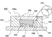
<execution mode 5 〉
Fig. 5 shows the light-emitting device 500 of present embodiment 5.The transparent member 102 of the light-emitting device 500 of present embodiment 5 has inclined plane 107 and with respect to the vertical plane 111 of upper surface 108 approximate vertical in its side.Inclined plane 107 forms has carried out the such shape of chamfering to the bight of flat transparent member.In the present embodiment, identical with execution mode 3, owing to do not have the bight of acute angle, therefore can the stress of abirritation on transparent member 102.In addition, because the bight has been carried out chamfering, can be suppressed at and produces space (void) in the light reflective resin 103.Owing to when forming light reflective resin 103, produce easily the space in the bight, therefore produce easily at the interface the space at transparent member 102 and light reflective resin 103.Yet if the at the interface generation space between transparent member 102 and light reflective resin 103 should can not reflected by the space by the light of boundary reflection, the light emission effciency reduces.As described in the transparent member 102 of present embodiment, carry out chamfering by across corner, can suppress the generation in space.
[embodiment]
Below, according to manufacture method of the present invention embodiments of the invention are elaborated.In addition, the present invention is not limited only to embodiment shown below certainly.
<embodiment 1 〉
Embodiment 1 is for the manufacture of light-emitting device shown in Figure 1.
(the first operation)
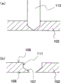
At first, light-emitting component 101 is placed on the substrate 104.In the present embodiment, substrate 104 uses aluminium nitride.Be on the surface of the aluminium nitride sheet material about 170W/mK in pyroconductivity, after the pattern printing of having carried out tungsten, burn till and form the wiring that is electrically connected with light-emitting component 101, form successively nickel, palladium, gold-plated thereon.In the wiring of this aluminium nitride set substrate, the protuberance that use is made of gold (bumps) 105, will be on Sapphire Substrate lamination semiconductor layer and the light-emitting component 101 of 1mm * 1mm of forming carries out the actual load of upside-down mounting chip as the mode of light-emitting face with sapphire substrate side.In addition, Fig. 1 shows single light-emitting device, carries out following the second~three operation by the pair set substrate during fabrication, carries out at last a sheet, thereby makes each light-emitting device.
(the second operation)
Then, the upper surface at light-emitting component 101 is combined in the transparent member 102 that the side has inclined plane 107.The inclined plane 107 that has the expansion from upper surface to lower surface in the circumferential lateral surface of transparent member 102.Upper surface and the lower surface of transparent member 102 form general planar, and the upper surface 108 of transparent member 102 and inclined plane 107 angulation θ 1 form 45 °.In the present embodiment, engagement member uses silicones, comes the Sapphire Substrate of bonding transparent member 102 and light-emitting component 101 by hot curing at composition surface 106a.Transparent member 102 in the present embodiment is the fluorophor plates that form by mixing YAG and aluminium oxide and sintering.Transparent member 102 is formed by inorganic material, therefore can obtain deteriorated less, light-emitting device that reliability is high.Because the area of the lower surface of transparent member 102 forms larger than the area of the upper surface of light-emitting component, transparent member 102 is engaged to have the mode of exposing face 106b of exposing from composition surface 106a.
(the 3rd operation)
Then, be shaped by transfer die, the inclined plane 107 of exposing face 106b and transparent member is covered by light reflective resin 103 one.In the present embodiment, light reflective resin 103 constitutes the titanium oxide that contains 30wt% in silicones.In addition, the pyroconductivity of light reflective resin 103 that contains the present embodiment of titanium oxide is about 1W/mK.The heat of transparent member 102 can be dispelled the heat efficiently via light reflective resin 103.In addition, the side 109 of light-emitting component 101 is also covered by light reflective resin 103 one with the inclined plane 107 of exposing face 106b and transparent member.
(the 4th operation)
At last, the set substrate after the processing of above-mentioned the first operation~the 3rd operation cut one by one cut off, thereby obtain the light-emitting device 100 of embodiment 1.
Like this, in the light-emitting device 100 of manufacturing, transparent member 102 is locked by light reflective resin 103, transparent member 102 can not come off, and in addition, the heat of transparent member 102 can be dispelled the heat efficiently via light reflective resin 103, therefore, can reduce the thermal resistance of light-emitting device.In addition, the area that makes on the one hand the upper surface 108 of transparent member 102 is that the light-emitting face of transparent member 102 is less, make on the other hand the contact area of transparent member 102 and light reflective resin 103 larger, thereby can obtain the light-emitting device of high brightness and thermal diffusivity excellence.In addition, even contain fluorophor, also can obtain the uneven few light-emitting device of form and aspect.
Industrial applicibility
The present invention can use in various light sources, such as backlight light source, signal lamp, on-vehicle parts, the billboard luminescent characters (channel letter) etc. of illumination light source, various indicating device (indicator) light source, vehicle mounted light source, display light source, liquid crystal.
Behind the embodiment that illustrates and describe various first-selections, the present invention should be apparent for those technical staff with general technical ability.Can predict the specific embodiment that the present invention is not limited to disclose, it is considered to concept of the present invention just is described, and should be interpreted as limited range of the present invention.The present invention is adapted at carrying out various modifications and variations in the defined invention scope of claim.The application is based on the TOHKEMY 2009-101519 communique of submitting on April 20th, 2009 and the TOHKEMY 2010-80156 communique of submitting on March 31st, 2010, and relevant content as a reference therewith.
Claims (16)
1. light-emitting device is characterized in that possessing:
Light-emitting component, with upper surface as light emitting surface;
Transparent member has upper surface and lower surface, the lower surface incident from the light of above-mentioned light-emitting component outgoing from this transparent member, and penetrate to the outside via the upper surface of this transparent member; And
The light reflective resin covers at least a portion of above-mentioned transparent member,
The circumferential lateral surface of above-mentioned transparent member has from the upper surface direction towards the inclined plane lower surface Directional Extension, that join with lower surface, and the area of the lower surface of above-mentioned transparent member forms larger than the area of the upper surface of above-mentioned light-emitting component,
The lower surface of above-mentioned transparent member and the upper surface of above-mentioned light-emitting component engage,
The part and the above-mentioned inclined plane that do not engage with above-mentioned light-emitting component in the lower surface of above-mentioned transparent member are covered by above-mentioned light reflective resin.
2. light-emitting device according to claim 1 is characterized in that,
The circumferential lateral surface of above-mentioned transparent member all forms the inclined plane.
3. light-emitting device according to claim 1 is characterized in that,
The circumferential lateral surface of above-mentioned transparent member begins until the centre of circumferential lateral surface forms vertical guide from upper surface, from this centre beginning until lower surface forms above-mentioned inclined plane.
4. light-emitting device according to claim 1 is characterized in that,
The upper surface of above-mentioned transparent member and lower surface are respectively the general planar faces, and form mutual almost parallel.
5. light-emitting device according to claim 4 is characterized in that,
The upper surface of above-mentioned transparent member forms and above-mentioned light reflective resin same plane roughly.
6. light-emitting device according to claim 1 is characterized in that,
Above-mentioned inclined plane is the general planar face.
7. light-emitting device according to claim 1 is characterized in that,
The lower surface of above-mentioned transparent member has:
The composition surface that engages with the upper surface of above-mentioned light-emitting component; And
That exposes from above-mentioned composition surface exposes face,
Above-mentioned transparent member expose face and above-mentioned inclined plane angulation θ
2Acute angle,
The upper surface of above-mentioned transparent member and above-mentioned inclined plane angulation θ
1Be the obtuse angle.
8. light-emitting device according to claim 7 is characterized in that,
The above-mentioned area that exposes face is 10%~100% of described composition surface with respect to the composition surface.
9. light-emitting device according to claim 1 is characterized in that,
Also possess substrate, this substrate is used for placing above-mentioned light-emitting component and light reflective resin.
10. light-emitting device according to claim 1 is characterized in that,
Above-mentioned transparent member constitutes and contains fluorophor.
11. light-emitting device according to claim 1 is characterized in that,
The side of above-mentioned light-emitting component is covered by above-mentioned light reflective resin.
12. light-emitting device according to claim 1 is characterized in that,
Above-mentioned light-emitting component is provided with pair of electrodes at the lower surface relative with its upper surface.
13. light-emitting device according to claim 1 is characterized in that,
Above-mentioned inclined plane accounts for more than 50% of circumferential lateral surface of above-mentioned transparent member.
14. a light-emitting device is characterized in that possessing:
Light-emitting component, with upper surface as light emitting surface;
Transparent member has upper surface and lower surface, the lower surface incident from the light of above-mentioned light-emitting component outgoing from this transparent member, and penetrate to the outside via the upper surface of this transparent member; And
The light reflective resin covers at least a portion of above-mentioned transparent member,
The circumferential lateral surface of above-mentioned transparent member begins until the centre of circumferential lateral surface forms the inclined plane from upper surface,
From this centre beginning until lower surface forms vertical guide,
The lower surface of above-mentioned transparent member and the upper surface of above-mentioned light-emitting component engage,
The part and the above-mentioned inclined plane that do not engage with above-mentioned light-emitting component in the lower surface of above-mentioned transparent member are covered by above-mentioned light reflective resin.
15. a light-emitting device is characterized in that possessing:
Light-emitting component, with upper surface as light emitting surface;
Transparent member has upper surface and lower surface, the lower surface incident from the light of above-mentioned light-emitting component outgoing from this transparent member, and penetrate to the outside via the upper surface of this transparent member; And
The light reflective resin covers at least a portion of above-mentioned transparent member,
The circumferential lateral surface of above-mentioned transparent member begins until the centre of circumferential lateral surface forms the inclined plane from upper surface,
Begin until lower surface forms to the anti-obliquity face of the direction inclination opposite with above-mentioned inclined plane from this centre,
The lower surface of above-mentioned transparent member and the upper surface of above-mentioned light-emitting component engage,
The part and the above-mentioned inclined plane that do not engage with above-mentioned light-emitting component in the lower surface of above-mentioned transparent member are covered by above-mentioned light reflective resin.
16. light-emitting device according to claim 15 is characterized in that,
Above-mentioned inclined plane and above-mentioned anti-obliquity face angulation are acute angle.
Applications Claiming Priority (4)
| Application Number | Priority Date | Filing Date | Title |
|---|---|---|---|
| JP2009101519 | 2009-04-20 | ||
| JP101519/2009 | 2009-04-20 | ||
| JP2010080156A JP5482378B2 (en) | 2009-04-20 | 2010-03-31 | Light emitting device |
| JP080156/2010 | 2010-03-31 |
Publications (2)
| Publication Number | Publication Date |
|---|---|
| CN101867003A CN101867003A (en) | 2010-10-20 |
| CN101867003B true CN101867003B (en) | 2013-01-16 |
Family
ID=42958636
Family Applications (1)
| Application Number | Title | Priority Date | Filing Date |
|---|---|---|---|
| CN2010101674925A Active CN101867003B (en) | 2009-04-20 | 2010-04-20 | Light emitting device |
Country Status (4)
| Country | Link |
|---|---|
| US (3) | US8330182B2 (en) |
| JP (1) | JP5482378B2 (en) |
| CN (1) | CN101867003B (en) |
| MY (2) | MY163993A (en) |
Families Citing this family (101)
| Publication number | Priority date | Publication date | Assignee | Title |
|---|---|---|---|---|
| JP2012033823A (en) | 2010-08-02 | 2012-02-16 | Stanley Electric Co Ltd | Light emitting device and method for manufacturing the same |
| TWI447969B (en) * | 2010-10-20 | 2014-08-01 | Interlight Optotech Corp | Light-emitting diode package structure |
| JP6369774B2 (en) * | 2010-10-29 | 2018-08-08 | 株式会社光波 | Light emitting device |
| KR20120066973A (en) * | 2010-12-15 | 2012-06-25 | 삼성엘이디 주식회사 | Light emitting device and manufacturing method of the same |
| KR20120100193A (en) * | 2011-03-03 | 2012-09-12 | 서울옵토디바이스주식회사 | Light emitting diode chip |
| JP5670249B2 (en) * | 2011-04-14 | 2015-02-18 | 日東電工株式会社 | Light emitting element transfer sheet manufacturing method, light emitting device manufacturing method, light emitting element transfer sheet, and light emitting device |
| JP5700544B2 (en) * | 2011-04-14 | 2015-04-15 | 日東電工株式会社 | Method for manufacturing light emitting diode device |
| JP5840377B2 (en) | 2011-04-14 | 2016-01-06 | 日東電工株式会社 | Reflective resin sheet and method for manufacturing light-emitting diode device |
| JP5745319B2 (en) * | 2011-04-14 | 2015-07-08 | 日東電工株式会社 | Fluorescent reflection sheet and method for manufacturing light emitting diode device |
| EP2701214A4 (en) * | 2011-04-20 | 2014-11-26 | Elm Inc | Light emitting device and method for manufacturing same |
| KR20120119350A (en) * | 2011-04-21 | 2012-10-31 | 삼성전자주식회사 | Light emitting device module and method for manufacturing the same |
| JP5680472B2 (en) * | 2011-04-22 | 2015-03-04 | シチズンホールディングス株式会社 | Manufacturing method of semiconductor light emitting device |
| KR101798884B1 (en) * | 2011-05-18 | 2017-11-17 | 삼성전자주식회사 | Light emitting device assembly and head light including the same |
| US9269878B2 (en) * | 2011-05-27 | 2016-02-23 | Lg Innotek Co., Ltd. | Light emitting device and light emitting apparatus |
| JP5840388B2 (en) * | 2011-06-01 | 2016-01-06 | 日東電工株式会社 | Light emitting diode device |
| KR101932951B1 (en) * | 2011-06-01 | 2018-12-27 | 루미리즈 홀딩 비.브이. | Method of attaching a light emitting device to a support substrate |
| JP5744643B2 (en) * | 2011-06-28 | 2015-07-08 | シチズン電子株式会社 | Method for manufacturing light emitting device |
| JP5893888B2 (en) * | 2011-10-13 | 2016-03-23 | シチズン電子株式会社 | Semiconductor light emitting device |
| JP5856816B2 (en) * | 2011-11-14 | 2016-02-10 | 株式会社小糸製作所 | Light emitting device |
| DE102012202555A1 (en) * | 2012-02-20 | 2013-08-22 | Osram Gmbh | LED ARRANGEMENT |
| DE102012102420B4 (en) * | 2012-03-21 | 2022-03-03 | OSRAM Opto Semiconductors Gesellschaft mit beschränkter Haftung | Process for producing an optoelectronic semiconductor component |
| JP5816127B2 (en) * | 2012-04-27 | 2015-11-18 | 株式会社東芝 | Semiconductor light emitting device and manufacturing method thereof |
| JP5837456B2 (en) * | 2012-05-28 | 2015-12-24 | 株式会社東芝 | Semiconductor light emitting device and light emitting module |
| US9562667B2 (en) * | 2012-08-02 | 2017-02-07 | Nichia Corporation | Wavelength converting device |
| JP2014078678A (en) | 2012-09-18 | 2014-05-01 | Toyoda Gosei Co Ltd | Semiconductor light-emitting device manufacturing method |
| KR101980230B1 (en) * | 2012-10-09 | 2019-09-02 | 삼성디스플레이 주식회사 | Array substrate for flexible display device and fabrication method thereof |
| CN104854716B (en) * | 2012-12-10 | 2017-06-20 | 西铁城时计株式会社 | LED matrix and its manufacture method |
| JP6097084B2 (en) | 2013-01-24 | 2017-03-15 | スタンレー電気株式会社 | Semiconductor light emitting device |
| JP6538306B2 (en) * | 2013-03-20 | 2019-07-03 | 株式会社半導体エネルギー研究所 | Light emitting module, light emitting device |
| JP2014225636A (en) * | 2013-04-16 | 2014-12-04 | 株式会社ディスコ | Light-emitting device |
| BR112015026316B1 (en) * | 2013-04-17 | 2022-01-11 | Koito Manufacturing Co., Ltd. | LIGHT EMITTING DEVICE |
| DE102013207111B4 (en) | 2013-04-19 | 2021-07-01 | OSRAM Opto Semiconductors Gesellschaft mit beschränkter Haftung | Optoelectronic component |
| CZ304579B6 (en) * | 2013-04-22 | 2014-07-16 | Crytur Spol. S R. O. | White light-emitting diode with monocrystalline luminophore and process for producing thereof |
| US9287472B2 (en) | 2013-06-27 | 2016-03-15 | Nichia Corporation | Light emitting device and method of manufacturing the same |
| KR102180388B1 (en) | 2013-07-08 | 2020-11-19 | 루미리즈 홀딩 비.브이. | Wavelength converted semiconductor light emitting device |
| JP6164038B2 (en) * | 2013-10-16 | 2017-07-19 | 豊田合成株式会社 | Light emitting device |
| EP3547379A1 (en) * | 2014-03-14 | 2019-10-02 | Citizen Electronics Co., Ltd. | Light emitting apparatus |
| JP6349904B2 (en) * | 2014-04-18 | 2018-07-04 | 日亜化学工業株式会社 | Semiconductor light emitting device and manufacturing method thereof |
| US10439111B2 (en) | 2014-05-14 | 2019-10-08 | Genesis Photonics Inc. | Light emitting device and manufacturing method thereof |
| US9997676B2 (en) | 2014-05-14 | 2018-06-12 | Genesis Photonics Inc. | Light emitting device and manufacturing method thereof |
| TWI557952B (en) | 2014-06-12 | 2016-11-11 | 新世紀光電股份有限公司 | Light emitting component |
| CN111816750A (en) * | 2014-06-19 | 2020-10-23 | 亮锐控股有限公司 | Wavelength converted light emitting device with small source size |
| JP6387773B2 (en) * | 2014-09-30 | 2018-09-12 | 日亜化学工業株式会社 | Method for manufacturing translucent member and method for manufacturing light emitting device |
| EP3239592B1 (en) * | 2014-11-18 | 2021-03-31 | Seoul Semiconductor Co., Ltd. | Light emitting device and vehicular lamp comprising same |
| WO2016094422A1 (en) * | 2014-12-08 | 2016-06-16 | Koninklijke Philips N.V. | Wavelength converted semiconductor light emitting device |
| TWI677113B (en) * | 2014-12-24 | 2019-11-11 | 晶元光電股份有限公司 | Light-emitting device and manufacturing method thereof |
| TWI649900B (en) * | 2015-02-04 | 2019-02-01 | 億光電子工業股份有限公司 | LED package structure and manufacturing method thereof |
| TWI657597B (en) * | 2015-03-18 | 2019-04-21 | 新世紀光電股份有限公司 | Edge lighting light emitting diode structure and method of manufacturing the same |
| CN105990498A (en) * | 2015-03-18 | 2016-10-05 | 新世纪光电股份有限公司 | Chip packaging structure and manufacturing method thereof |
| CN110767793A (en) * | 2015-05-05 | 2020-02-07 | 新世纪光电股份有限公司 | Light emitting device and method for manufacturing the same |
| JP6179555B2 (en) | 2015-06-01 | 2017-08-16 | 日亜化学工業株式会社 | Light emitting device |
| KR102335106B1 (en) * | 2015-06-19 | 2021-12-03 | 삼성전자 주식회사 | Light Emitting Diode package and Method of manufacturing the same |
| JP6481559B2 (en) | 2015-08-18 | 2019-03-13 | 日亜化学工業株式会社 | Light emitting device |
| JP6327220B2 (en) | 2015-08-31 | 2018-05-23 | 日亜化学工業株式会社 | Light emitting device |
| CN106549092A (en) | 2015-09-18 | 2017-03-29 | 新世纪光电股份有限公司 | Light emitting device and method for manufacturing the same |
| JP6249002B2 (en) * | 2015-09-30 | 2017-12-20 | 日亜化学工業株式会社 | Method for manufacturing light emitting device |
| CN106601898A (en) * | 2015-10-19 | 2017-04-26 | 展晶科技(深圳)有限公司 | Light-emitting diode packaging structure |
| EP3174110B1 (en) | 2015-11-30 | 2020-12-23 | Nichia Corporation | Light emitting device |
| JP6332294B2 (en) * | 2015-11-30 | 2018-05-30 | 日亜化学工業株式会社 | Light emitting device |
| JP6399017B2 (en) | 2016-02-29 | 2018-10-03 | 日亜化学工業株式会社 | Light emitting device |
| JP6754206B2 (en) * | 2016-03-28 | 2020-09-09 | シチズン時計株式会社 | Light emitting device |
| JP2017183427A (en) * | 2016-03-29 | 2017-10-05 | 豊田合成株式会社 | Light-emitting device |
| WO2017176213A1 (en) * | 2016-04-08 | 2017-10-12 | Heptagon Micro Optics Pte. Ltd. | Thin optoelectronic modules with apertures and their manufacture |
| JP6432559B2 (en) * | 2016-05-17 | 2018-12-05 | カシオ計算機株式会社 | Phosphor device, lighting apparatus and projector apparatus |
| JP6724639B2 (en) | 2016-08-01 | 2020-07-15 | 日亜化学工業株式会社 | Light emitting device |
| CN107946441A (en) | 2016-10-12 | 2018-04-20 | 亿光电子工业股份有限公司 | Light-emitting device and light-emitting diode encapsulation structure |
| TWI651870B (en) | 2016-10-19 | 2019-02-21 | 新世紀光電股份有限公司 | Light emitting device and method of manufacturing same |
| JP6789778B2 (en) * | 2016-11-25 | 2020-11-25 | スタンレー電気株式会社 | Semiconductor light emitting device and its manufacturing method |
| JP6776859B2 (en) | 2016-12-09 | 2020-10-28 | 日本電気硝子株式会社 | Manufacturing method of wavelength conversion member, wavelength conversion member and light emitting device |
| DE102017101729A1 (en) * | 2017-01-30 | 2018-08-02 | Osram Opto Semiconductors Gmbh | Radiation-emitting device |
| JP6579141B2 (en) | 2017-03-24 | 2019-09-25 | 日亜化学工業株式会社 | Light emitting device and method for manufacturing light emitting device |
| JP7082270B2 (en) * | 2017-08-28 | 2022-06-08 | 日亜化学工業株式会社 | Light emitting device |
| JP6575576B2 (en) * | 2017-10-12 | 2019-09-18 | 日亜化学工業株式会社 | Method for manufacturing light emitting device |
| JP6897729B2 (en) * | 2017-10-12 | 2021-07-07 | 日亜化学工業株式会社 | Manufacturing method of light emitting device |
| TW202249306A (en) | 2017-11-05 | 2022-12-16 | 新世紀光電股份有限公司 | Light emitting apparatus |
| TW201919261A (en) | 2017-11-05 | 2019-05-16 | 新世紀光電股份有限公司 | Light emitting device |
| JP7221659B2 (en) * | 2017-11-17 | 2023-02-14 | スタンレー電気株式会社 | semiconductor light emitting device |
| JP6729537B2 (en) * | 2017-11-20 | 2020-07-22 | 日亜化学工業株式会社 | Light emitting device and manufacturing method thereof |
| JP7235944B2 (en) * | 2018-02-21 | 2023-03-09 | 日亜化学工業株式会社 | Light-emitting device and method for manufacturing light-emitting device |
| CN110323213A (en) * | 2018-03-30 | 2019-10-11 | 日亚化学工业株式会社 | The manufacturing method of light emitting device |
| JP7117127B2 (en) | 2018-04-02 | 2022-08-12 | スタンレー電気株式会社 | light emitting device |
| EP3608959B1 (en) | 2018-08-06 | 2023-11-15 | Nichia Corporation | Light emitting device and method for manufacturing same |
| JP6989782B2 (en) * | 2018-08-06 | 2022-02-03 | 日亜化学工業株式会社 | Light emitting device and its manufacturing method |
| JP6940776B2 (en) * | 2018-11-05 | 2021-09-29 | 日亜化学工業株式会社 | Light emitting device and its manufacturing method |
| CN109802015B (en) * | 2018-12-25 | 2024-02-20 | 广东晶科电子股份有限公司 | Semiconductor device and packaging method thereof |
| JP6784287B2 (en) * | 2018-12-27 | 2020-11-11 | 日亜化学工業株式会社 | Light emitting device and its manufacturing method |
| EP3956925A1 (en) | 2019-04-18 | 2022-02-23 | Lumileds Holding B.V. | Lighting device |
| JP7257247B2 (en) * | 2019-05-16 | 2023-04-13 | スタンレー電気株式会社 | light emitting device |
| JP7288343B2 (en) | 2019-05-16 | 2023-06-07 | スタンレー電気株式会社 | light emitting device |
| JP7267836B2 (en) * | 2019-05-16 | 2023-05-02 | スタンレー電気株式会社 | light emitting device |
| JP2020188185A (en) * | 2019-05-16 | 2020-11-19 | スタンレー電気株式会社 | Light-emitting device |
| EP3905316B1 (en) * | 2019-11-14 | 2023-08-30 | Nuvoton Technology Corporation Japan | Light-emitting device |
| JP6793899B1 (en) | 2019-11-14 | 2020-12-02 | ヌヴォトンテクノロジージャパン株式会社 | Light emitting device |
| JP7060810B2 (en) | 2019-11-19 | 2022-04-27 | 日亜化学工業株式会社 | Light emitting device and manufacturing method of light emitting device |
| JP7108196B2 (en) * | 2019-12-26 | 2022-07-28 | 日亜化学工業株式会社 | Light-emitting device, method for manufacturing wavelength conversion member, and method for manufacturing light-emitting device |
| JP7060819B2 (en) * | 2020-07-01 | 2022-04-27 | 日亜化学工業株式会社 | Light emitting device |
| JP6989807B2 (en) * | 2020-07-08 | 2022-02-03 | 日亜化学工業株式会社 | Light emitting device and its manufacturing method |
| DE102020125056A1 (en) * | 2020-09-25 | 2022-03-31 | OSRAM Opto Semiconductors Gesellschaft mit beschränkter Haftung | OPTOELECTRONIC DEVICE AND METHOD FOR MANUFACTURING OPTOELECTRONIC DEVICE |
| US20220102597A1 (en) * | 2020-09-28 | 2022-03-31 | Tek Beng Low | Light emitting devices having profiled side surfaces |
| JP7044990B2 (en) * | 2020-12-03 | 2022-03-31 | 日亜化学工業株式会社 | Light emitting device |
| US20230288037A1 (en) * | 2022-03-14 | 2023-09-14 | Usai, Llc | Flush Glass Adjustable Lighting Fixture |
Citations (1)
| Publication number | Priority date | Publication date | Assignee | Title |
|---|---|---|---|---|
| CN1971956A (en) * | 2005-11-21 | 2007-05-30 | 夏普株式会社 | Light emitting device |
Family Cites Families (7)
| Publication number | Priority date | Publication date | Assignee | Title |
|---|---|---|---|---|
| JP4280050B2 (en) * | 2002-10-07 | 2009-06-17 | シチズン電子株式会社 | White light emitting device |
| JP4020092B2 (en) | 2004-03-16 | 2007-12-12 | 住友電気工業株式会社 | Semiconductor light emitting device |
| JP4516337B2 (en) * | 2004-03-25 | 2010-08-04 | シチズン電子株式会社 | Semiconductor light emitting device |
| JP2007019096A (en) * | 2005-07-05 | 2007-01-25 | Toyoda Gosei Co Ltd | Light-emitting device and its manufacturing method |
| JP4948818B2 (en) | 2005-10-28 | 2012-06-06 | 京セラ株式会社 | Light emitting device and lighting device |
| JP5155555B2 (en) | 2006-12-07 | 2013-03-06 | 日本電気硝子株式会社 | Optical component and light emitting device using the same |
| KR101517644B1 (en) * | 2007-11-29 | 2015-05-04 | 니치아 카가쿠 고교 가부시키가이샤 | Light-emitting device and its manufacturing method |
-
2010
- 2010-03-31 JP JP2010080156A patent/JP5482378B2/en active Active
- 2010-04-19 US US12/662,474 patent/US8330182B2/en active Active
- 2010-04-20 MY MYPI2010001779A patent/MY163993A/en unknown
- 2010-04-20 MY MYPI2015000952A patent/MY168492A/en unknown
- 2010-04-20 CN CN2010101674925A patent/CN101867003B/en active Active
-
2012
- 2012-11-02 US US13/667,695 patent/US8525218B2/en active Active
-
2013
- 2013-08-02 US US13/958,238 patent/US8921882B2/en active Active
Patent Citations (1)
| Publication number | Priority date | Publication date | Assignee | Title |
|---|---|---|---|---|
| CN1971956A (en) * | 2005-11-21 | 2007-05-30 | 夏普株式会社 | Light emitting device |
Non-Patent Citations (1)
| Title |
|---|
| JP特开2007-19096A 2007.01.25 |
Also Published As
| Publication number | Publication date |
|---|---|
| MY168492A (en) | 2018-11-12 |
| JP5482378B2 (en) | 2014-05-07 |
| JP2010272847A (en) | 2010-12-02 |
| MY163993A (en) | 2017-11-15 |
| US8330182B2 (en) | 2012-12-11 |
| US8525218B2 (en) | 2013-09-03 |
| US20130313602A1 (en) | 2013-11-28 |
| US20100264438A1 (en) | 2010-10-21 |
| CN101867003A (en) | 2010-10-20 |
| US20130056781A1 (en) | 2013-03-07 |
| US8921882B2 (en) | 2014-12-30 |
Similar Documents
| Publication | Publication Date | Title |
|---|---|---|
| CN101867003B (en) | Light emitting device | |
| US10141491B2 (en) | Method of manufacturing light emitting device | |
| JP6444299B2 (en) | Light emitting device | |
| US10274140B1 (en) | Method for manufacturing light emitting device | |
| JP5278023B2 (en) | Method for manufacturing light emitting device | |
| TWI482307B (en) | Illumination structure | |
| JP2010272847A5 (en) | ||
| US8558259B2 (en) | Optoelectronic component having a dome-like conversion element | |
| US20150014711A1 (en) | Optoelectronic component with inert gas atmosphere | |
| KR20190010478A (en) | Light-emitting device, integrated light-emitting device and light-emitting module | |
| JP6481559B2 (en) | Light emitting device | |
| CN102138230A (en) | Optoelectronic component | |
| JP2019079873A (en) | Light emitting module and integrated light emitting module | |
| JP2019016763A (en) | Light-emitting device and method for manufacturing the same | |
| JP2007059781A (en) | Submount-attached light emitting element and light emitting device | |
| JP2013175759A (en) | Manufacturing method of light emitting device | |
| JP2019145690A (en) | Light-emitting device and manufacturing method of light-emitting device | |
| CN117673232A (en) | Light emitting device | |
| US11843078B2 (en) | Light emitting device with good visibility | |
| JP2018022723A (en) | Light emitting device | |
| JP7147138B2 (en) | Light-emitting device, lighting device, image display device, and vehicle indicator light | |
| KR20180005450A (en) | Flash module, camera module and mobile device including the same | |
| JP2005229136A (en) | Light-emitting device and method of manufacturing the same | |
| US11050007B2 (en) | Light emitting device | |
| JP2020150286A (en) | Light emitting device |
Legal Events
| Date | Code | Title | Description |
|---|---|---|---|
| C06 | Publication | ||
| PB01 | Publication | ||
| C10 | Entry into substantive examination | ||
| SE01 | Entry into force of request for substantive examination | ||
| C14 | Grant of patent or utility model | ||
| GR01 | Patent grant |