CN101853809B - Semiconductor element and manufacturing method and liquid-crystal display device and manufacturing method thereof - Google Patents
Semiconductor element and manufacturing method and liquid-crystal display device and manufacturing method thereof Download PDFInfo
- Publication number
- CN101853809B CN101853809B CN201010167923.8A CN201010167923A CN101853809B CN 101853809 B CN101853809 B CN 101853809B CN 201010167923 A CN201010167923 A CN 201010167923A CN 101853809 B CN101853809 B CN 101853809B
- Authority
- CN
- China
- Prior art keywords
- film
- layer
- semiconductor film
- dielectric film
- semiconductor
- Prior art date
- Legal status (The legal status is an assumption and is not a legal conclusion. Google has not performed a legal analysis and makes no representation as to the accuracy of the status listed.)
- Expired - Fee Related
Links
- 239000004065 semiconductor Substances 0.000 title claims abstract description 181
- 238000004519 manufacturing process Methods 0.000 title claims description 41
- 239000004973 liquid crystal related substance Substances 0.000 title description 28
- 238000000034 method Methods 0.000 claims abstract description 196
- 239000000463 material Substances 0.000 claims abstract description 55
- 238000007599 discharging Methods 0.000 claims abstract description 19
- 239000000758 substrate Substances 0.000 claims description 87
- 239000002131 composite material Substances 0.000 claims description 72
- 239000004020 conductor Substances 0.000 claims description 61
- 239000012535 impurity Substances 0.000 claims description 34
- VYPSYNLAJGMNEJ-UHFFFAOYSA-N silicon dioxide Inorganic materials O=[Si]=O VYPSYNLAJGMNEJ-UHFFFAOYSA-N 0.000 claims description 34
- 239000010936 titanium Substances 0.000 claims description 32
- 230000015572 biosynthetic process Effects 0.000 claims description 31
- 229910052719 titanium Inorganic materials 0.000 claims description 31
- RTAQQCXQSZGOHL-UHFFFAOYSA-N Titanium Chemical compound [Ti] RTAQQCXQSZGOHL-UHFFFAOYSA-N 0.000 claims description 30
- OGIDPMRJRNCKJF-UHFFFAOYSA-N titanium oxide Inorganic materials [Ti]=O OGIDPMRJRNCKJF-UHFFFAOYSA-N 0.000 claims description 25
- GWEVSGVZZGPLCZ-UHFFFAOYSA-N Titan oxide Chemical compound O=[Ti]=O GWEVSGVZZGPLCZ-UHFFFAOYSA-N 0.000 claims description 24
- 239000004642 Polyimide Substances 0.000 claims description 17
- 229920001721 polyimide Polymers 0.000 claims description 17
- 239000000377 silicon dioxide Substances 0.000 claims description 17
- XLOMVQKBTHCTTD-UHFFFAOYSA-N Zinc monoxide Chemical compound [Zn]=O XLOMVQKBTHCTTD-UHFFFAOYSA-N 0.000 claims description 14
- 229920002120 photoresistant polymer Polymers 0.000 claims description 14
- SMZOUWXMTYCWNB-UHFFFAOYSA-N 2-(2-methoxy-5-methylphenyl)ethanamine Chemical compound COC1=CC=C(C)C=C1CCN SMZOUWXMTYCWNB-UHFFFAOYSA-N 0.000 claims description 12
- NIXOWILDQLNWCW-UHFFFAOYSA-N 2-Propenoic acid Natural products OC(=O)C=C NIXOWILDQLNWCW-UHFFFAOYSA-N 0.000 claims description 12
- 239000011248 coating agent Substances 0.000 claims description 10
- 238000000576 coating method Methods 0.000 claims description 10
- 239000002245 particle Substances 0.000 claims description 10
- 230000004888 barrier function Effects 0.000 claims description 9
- 238000009832 plasma treatment Methods 0.000 claims description 9
- 238000010276 construction Methods 0.000 claims description 8
- 239000001257 hydrogen Substances 0.000 claims description 7
- 229910052739 hydrogen Inorganic materials 0.000 claims description 7
- 125000004435 hydrogen atom Chemical group [H]* 0.000 claims description 6
- 125000000217 alkyl group Chemical group 0.000 claims description 5
- 125000003118 aryl group Chemical group 0.000 claims description 5
- 125000001424 substituent group Chemical group 0.000 claims description 5
- 238000009713 electroplating Methods 0.000 claims description 4
- 229910052725 zinc Inorganic materials 0.000 claims description 3
- 239000011701 zinc Substances 0.000 claims description 3
- HCHKCACWOHOZIP-UHFFFAOYSA-N Zinc Chemical compound [Zn] HCHKCACWOHOZIP-UHFFFAOYSA-N 0.000 claims description 2
- AJNVQOSZGJRYEI-UHFFFAOYSA-N digallium;oxygen(2-) Chemical compound [O-2].[O-2].[O-2].[Ga+3].[Ga+3] AJNVQOSZGJRYEI-UHFFFAOYSA-N 0.000 claims description 2
- 229910001195 gallium oxide Inorganic materials 0.000 claims description 2
- 150000002222 fluorine compounds Chemical group 0.000 claims 2
- 230000008569 process Effects 0.000 abstract description 59
- 229910052751 metal Inorganic materials 0.000 abstract description 13
- 239000002184 metal Substances 0.000 abstract description 13
- 239000010408 film Substances 0.000 description 313
- 239000010410 layer Substances 0.000 description 108
- 238000005530 etching Methods 0.000 description 36
- 239000007789 gas Substances 0.000 description 29
- 238000002347 injection Methods 0.000 description 19
- 239000007924 injection Substances 0.000 description 19
- 230000003647 oxidation Effects 0.000 description 19
- 238000007254 oxidation reaction Methods 0.000 description 19
- -1 siloxanes Chemical class 0.000 description 19
- 229910052581 Si3N4 Inorganic materials 0.000 description 18
- XUIMIQQOPSSXEZ-UHFFFAOYSA-N Silicon Chemical compound [Si] XUIMIQQOPSSXEZ-UHFFFAOYSA-N 0.000 description 18
- 230000014509 gene expression Effects 0.000 description 18
- 229910052710 silicon Inorganic materials 0.000 description 18
- 239000010703 silicon Substances 0.000 description 18
- HQVNEWCFYHHQES-UHFFFAOYSA-N silicon nitride Chemical compound N12[Si]34N5[Si]62N3[Si]51N64 HQVNEWCFYHHQES-UHFFFAOYSA-N 0.000 description 18
- 239000011347 resin Substances 0.000 description 17
- 229920005989 resin Polymers 0.000 description 17
- 239000010409 thin film Substances 0.000 description 16
- 239000010949 copper Substances 0.000 description 13
- 239000012212 insulator Substances 0.000 description 13
- 239000007788 liquid Substances 0.000 description 13
- 150000002894 organic compounds Chemical class 0.000 description 12
- QVGXLLKOCUKJST-UHFFFAOYSA-N atomic oxygen Chemical compound [O] QVGXLLKOCUKJST-UHFFFAOYSA-N 0.000 description 11
- 239000001301 oxygen Substances 0.000 description 11
- 229910052760 oxygen Inorganic materials 0.000 description 11
- 238000007781 pre-processing Methods 0.000 description 11
- LIVNPJMFVYWSIS-UHFFFAOYSA-N silicon monoxide Chemical compound [Si-]#[O+] LIVNPJMFVYWSIS-UHFFFAOYSA-N 0.000 description 11
- 239000004372 Polyvinyl alcohol Substances 0.000 description 10
- 238000010586 diagram Methods 0.000 description 10
- 230000037230 mobility Effects 0.000 description 10
- 229920002451 polyvinyl alcohol Polymers 0.000 description 10
- 239000002904 solvent Substances 0.000 description 10
- 230000006870 function Effects 0.000 description 9
- 238000005401 electroluminescence Methods 0.000 description 8
- 239000011159 matrix material Substances 0.000 description 8
- 238000004544 sputter deposition Methods 0.000 description 8
- PNEYBMLMFCGWSK-UHFFFAOYSA-N Alumina Chemical compound [O-2].[O-2].[O-2].[Al+3].[Al+3] PNEYBMLMFCGWSK-UHFFFAOYSA-N 0.000 description 7
- 239000004952 Polyamide Substances 0.000 description 7
- 238000013461 design Methods 0.000 description 7
- 229920002647 polyamide Polymers 0.000 description 7
- IJGRMHOSHXDMSA-UHFFFAOYSA-N Atomic nitrogen Chemical compound N#N IJGRMHOSHXDMSA-UHFFFAOYSA-N 0.000 description 6
- OKTJSMMVPCPJKN-UHFFFAOYSA-N Carbon Chemical compound [C] OKTJSMMVPCPJKN-UHFFFAOYSA-N 0.000 description 6
- PXHVJJICTQNCMI-UHFFFAOYSA-N Nickel Chemical compound [Ni] PXHVJJICTQNCMI-UHFFFAOYSA-N 0.000 description 6
- 239000012298 atmosphere Substances 0.000 description 6
- 239000000460 chlorine Substances 0.000 description 6
- 229910052802 copper Inorganic materials 0.000 description 6
- 239000000203 mixture Substances 0.000 description 6
- 229910021332 silicide Inorganic materials 0.000 description 6
- FVBUAEGBCNSCDD-UHFFFAOYSA-N silicide(4-) Chemical compound [Si-4] FVBUAEGBCNSCDD-UHFFFAOYSA-N 0.000 description 6
- 229910052709 silver Inorganic materials 0.000 description 6
- RYGMFSIKBFXOCR-UHFFFAOYSA-N Copper Chemical compound [Cu] RYGMFSIKBFXOCR-UHFFFAOYSA-N 0.000 description 5
- 229910018557 Si O Inorganic materials 0.000 description 5
- 229910052782 aluminium Inorganic materials 0.000 description 5
- 230000005540 biological transmission Effects 0.000 description 5
- 229910052799 carbon Inorganic materials 0.000 description 5
- 238000001035 drying Methods 0.000 description 5
- 230000000694 effects Effects 0.000 description 5
- 229910052738 indium Inorganic materials 0.000 description 5
- 239000002105 nanoparticle Substances 0.000 description 5
- 238000012545 processing Methods 0.000 description 5
- 239000002994 raw material Substances 0.000 description 5
- 230000027756 respiratory electron transport chain Effects 0.000 description 5
- 239000004332 silver Substances 0.000 description 5
- 125000006850 spacer group Chemical group 0.000 description 5
- 238000004528 spin coating Methods 0.000 description 5
- 239000011787 zinc oxide Substances 0.000 description 5
- WUPHOULIZUERAE-UHFFFAOYSA-N 3-(oxolan-2-yl)propanoic acid Chemical compound OC(=O)CCC1CCCO1 WUPHOULIZUERAE-UHFFFAOYSA-N 0.000 description 4
- ZOXJGFHDIHLPTG-UHFFFAOYSA-N Boron Chemical compound [B] ZOXJGFHDIHLPTG-UHFFFAOYSA-N 0.000 description 4
- KRHYYFGTRYWZRS-UHFFFAOYSA-M Fluoride anion Chemical compound [F-] KRHYYFGTRYWZRS-UHFFFAOYSA-M 0.000 description 4
- UQSXHKLRYXJYBZ-UHFFFAOYSA-N Iron oxide Chemical compound [Fe]=O UQSXHKLRYXJYBZ-UHFFFAOYSA-N 0.000 description 4
- 229910003902 SiCl 4 Inorganic materials 0.000 description 4
- BQCADISMDOOEFD-UHFFFAOYSA-N Silver Chemical compound [Ag] BQCADISMDOOEFD-UHFFFAOYSA-N 0.000 description 4
- MCMNRKCIXSYSNV-UHFFFAOYSA-N Zirconium dioxide Chemical compound O=[Zr]=O MCMNRKCIXSYSNV-UHFFFAOYSA-N 0.000 description 4
- XAGFODPZIPBFFR-UHFFFAOYSA-N aluminium Chemical compound [Al] XAGFODPZIPBFFR-UHFFFAOYSA-N 0.000 description 4
- 229910052796 boron Inorganic materials 0.000 description 4
- 229910052980 cadmium sulfide Inorganic materials 0.000 description 4
- 239000013078 crystal Substances 0.000 description 4
- 210000002858 crystal cell Anatomy 0.000 description 4
- 230000009977 dual effect Effects 0.000 description 4
- 238000011049 filling Methods 0.000 description 4
- 230000004907 flux Effects 0.000 description 4
- 239000010931 gold Substances 0.000 description 4
- 238000003384 imaging method Methods 0.000 description 4
- MRNHPUHPBOKKQT-UHFFFAOYSA-N indium;tin;hydrate Chemical compound O.[In].[Sn] MRNHPUHPBOKKQT-UHFFFAOYSA-N 0.000 description 4
- 230000003993 interaction Effects 0.000 description 4
- XEEYBQQBJWHFJM-UHFFFAOYSA-N iron Substances [Fe] XEEYBQQBJWHFJM-UHFFFAOYSA-N 0.000 description 4
- 239000012528 membrane Substances 0.000 description 4
- 239000003960 organic solvent Substances 0.000 description 4
- 238000005268 plasma chemical vapour deposition Methods 0.000 description 4
- ZWEHNKRNPOVVGH-UHFFFAOYSA-N 2-Butanone Chemical compound CCC(C)=O ZWEHNKRNPOVVGH-UHFFFAOYSA-N 0.000 description 3
- XEKOWRVHYACXOJ-UHFFFAOYSA-N Ethyl acetate Chemical compound CCOC(C)=O XEKOWRVHYACXOJ-UHFFFAOYSA-N 0.000 description 3
- KFZMGEQAYNKOFK-UHFFFAOYSA-N Isopropanol Chemical compound CC(C)O KFZMGEQAYNKOFK-UHFFFAOYSA-N 0.000 description 3
- KDLHZDBZIXYQEI-UHFFFAOYSA-N Palladium Chemical compound [Pd] KDLHZDBZIXYQEI-UHFFFAOYSA-N 0.000 description 3
- ZLMJMSJWJFRBEC-UHFFFAOYSA-N Potassium Chemical compound [K] ZLMJMSJWJFRBEC-UHFFFAOYSA-N 0.000 description 3
- ATJFFYVFTNAWJD-UHFFFAOYSA-N Tin Chemical compound [Sn] ATJFFYVFTNAWJD-UHFFFAOYSA-N 0.000 description 3
- 239000000853 adhesive Substances 0.000 description 3
- 230000001070 adhesive effect Effects 0.000 description 3
- 239000004411 aluminium Substances 0.000 description 3
- 238000004380 ashing Methods 0.000 description 3
- 125000004429 atom Chemical group 0.000 description 3
- 230000008901 benefit Effects 0.000 description 3
- 230000000903 blocking effect Effects 0.000 description 3
- 238000005229 chemical vapour deposition Methods 0.000 description 3
- 230000008878 coupling Effects 0.000 description 3
- 238000010168 coupling process Methods 0.000 description 3
- 238000005859 coupling reaction Methods 0.000 description 3
- 239000002270 dispersing agent Substances 0.000 description 3
- PCHJSUWPFVWCPO-UHFFFAOYSA-N gold Chemical compound [Au] PCHJSUWPFVWCPO-UHFFFAOYSA-N 0.000 description 3
- 229910052737 gold Inorganic materials 0.000 description 3
- 150000002484 inorganic compounds Chemical class 0.000 description 3
- 229910010272 inorganic material Inorganic materials 0.000 description 3
- 238000003475 lamination Methods 0.000 description 3
- 238000004518 low pressure chemical vapour deposition Methods 0.000 description 3
- 239000003595 mist Substances 0.000 description 3
- 238000002156 mixing Methods 0.000 description 3
- 229910052757 nitrogen Inorganic materials 0.000 description 3
- 230000001699 photocatalysis Effects 0.000 description 3
- 238000007146 photocatalysis Methods 0.000 description 3
- 238000001020 plasma etching Methods 0.000 description 3
- BASFCYQUMIYNBI-UHFFFAOYSA-N platinum Chemical compound [Pt] BASFCYQUMIYNBI-UHFFFAOYSA-N 0.000 description 3
- 238000005498 polishing Methods 0.000 description 3
- 229910052700 potassium Inorganic materials 0.000 description 3
- 239000011591 potassium Substances 0.000 description 3
- 239000000243 solution Substances 0.000 description 3
- 229910052718 tin Inorganic materials 0.000 description 3
- 238000005406 washing Methods 0.000 description 3
- HYZJCKYKOHLVJF-UHFFFAOYSA-N 1H-benzimidazole Chemical compound C1=CC=C2NC=NC2=C1 HYZJCKYKOHLVJF-UHFFFAOYSA-N 0.000 description 2
- CSCPPACGZOOCGX-UHFFFAOYSA-N Acetone Chemical compound CC(C)=O CSCPPACGZOOCGX-UHFFFAOYSA-N 0.000 description 2
- XKRFYHLGVUSROY-UHFFFAOYSA-N Argon Chemical compound [Ar] XKRFYHLGVUSROY-UHFFFAOYSA-N 0.000 description 2
- ZAMOUSCENKQFHK-UHFFFAOYSA-N Chlorine atom Chemical compound [Cl] ZAMOUSCENKQFHK-UHFFFAOYSA-N 0.000 description 2
- LFQSCWFLJHTTHZ-UHFFFAOYSA-N Ethanol Chemical compound CCO LFQSCWFLJHTTHZ-UHFFFAOYSA-N 0.000 description 2
- KRHYYFGTRYWZRS-UHFFFAOYSA-N Fluorane Chemical compound F KRHYYFGTRYWZRS-UHFFFAOYSA-N 0.000 description 2
- GYHNNYVSQQEPJS-UHFFFAOYSA-N Gallium Chemical compound [Ga] GYHNNYVSQQEPJS-UHFFFAOYSA-N 0.000 description 2
- 229910000577 Silicon-germanium Inorganic materials 0.000 description 2
- 229910002367 SrTiO Inorganic materials 0.000 description 2
- NRTOMJZYCJJWKI-UHFFFAOYSA-N Titanium nitride Chemical compound [Ti]#N NRTOMJZYCJJWKI-UHFFFAOYSA-N 0.000 description 2
- 229910052786 argon Inorganic materials 0.000 description 2
- UMIVXZPTRXBADB-UHFFFAOYSA-N benzocyclobutene Chemical compound C1=CC=C2CCC2=C1 UMIVXZPTRXBADB-UHFFFAOYSA-N 0.000 description 2
- AQCDIIAORKRFCD-UHFFFAOYSA-N cadmium selenide Chemical compound [Cd]=[Se] AQCDIIAORKRFCD-UHFFFAOYSA-N 0.000 description 2
- 229910052791 calcium Inorganic materials 0.000 description 2
- 239000011575 calcium Substances 0.000 description 2
- 239000003795 chemical substances by application Substances 0.000 description 2
- 229910052801 chlorine Inorganic materials 0.000 description 2
- 239000011651 chromium Substances 0.000 description 2
- 238000000151 deposition Methods 0.000 description 2
- 230000008021 deposition Effects 0.000 description 2
- 229910052733 gallium Inorganic materials 0.000 description 2
- 229910052732 germanium Inorganic materials 0.000 description 2
- GNPVGFCGXDBREM-UHFFFAOYSA-N germanium atom Chemical compound [Ge] GNPVGFCGXDBREM-UHFFFAOYSA-N 0.000 description 2
- 239000011521 glass Substances 0.000 description 2
- 238000010438 heat treatment Methods 0.000 description 2
- 229910052734 helium Inorganic materials 0.000 description 2
- APFVFJFRJDLVQX-UHFFFAOYSA-N indium atom Chemical compound [In] APFVFJFRJDLVQX-UHFFFAOYSA-N 0.000 description 2
- 229910003437 indium oxide Inorganic materials 0.000 description 2
- PJXISJQVUVHSOJ-UHFFFAOYSA-N indium(iii) oxide Chemical compound [O-2].[O-2].[O-2].[In+3].[In+3] PJXISJQVUVHSOJ-UHFFFAOYSA-N 0.000 description 2
- 239000011810 insulating material Substances 0.000 description 2
- 238000009413 insulation Methods 0.000 description 2
- 239000011229 interlayer Substances 0.000 description 2
- 229910052759 nickel Inorganic materials 0.000 description 2
- 229910052758 niobium Inorganic materials 0.000 description 2
- 239000010955 niobium Substances 0.000 description 2
- URLJKFSTXLNXLG-UHFFFAOYSA-N niobium(5+);oxygen(2-) Chemical compound [O-2].[O-2].[O-2].[O-2].[O-2].[Nb+5].[Nb+5] URLJKFSTXLNXLG-UHFFFAOYSA-N 0.000 description 2
- 238000007747 plating Methods 0.000 description 2
- 238000007639 printing Methods 0.000 description 2
- 239000010948 rhodium Substances 0.000 description 2
- 239000000565 sealant Substances 0.000 description 2
- 229910052814 silicon oxide Inorganic materials 0.000 description 2
- 238000005507 spraying Methods 0.000 description 2
- 230000006641 stabilisation Effects 0.000 description 2
- 238000011105 stabilization Methods 0.000 description 2
- 238000003860 storage Methods 0.000 description 2
- 229910052712 strontium Inorganic materials 0.000 description 2
- CIOAGBVUUVVLOB-UHFFFAOYSA-N strontium atom Chemical compound [Sr] CIOAGBVUUVVLOB-UHFFFAOYSA-N 0.000 description 2
- 229910052721 tungsten Inorganic materials 0.000 description 2
- ZNOKGRXACCSDPY-UHFFFAOYSA-N tungsten trioxide Chemical compound O=[W](=O)=O ZNOKGRXACCSDPY-UHFFFAOYSA-N 0.000 description 2
- XLYOFNOQVPJJNP-UHFFFAOYSA-N water Substances O XLYOFNOQVPJJNP-UHFFFAOYSA-N 0.000 description 2
- 229910052726 zirconium Inorganic materials 0.000 description 2
- 229910017073 AlLi Inorganic materials 0.000 description 1
- 229910017083 AlN Inorganic materials 0.000 description 1
- PIGFYZPCRLYGLF-UHFFFAOYSA-N Aluminum nitride Chemical compound [Al]#N PIGFYZPCRLYGLF-UHFFFAOYSA-N 0.000 description 1
- DKPFZGUDAPQIHT-UHFFFAOYSA-N Butyl acetate Natural products CCCCOC(C)=O DKPFZGUDAPQIHT-UHFFFAOYSA-N 0.000 description 1
- OYPRJOBELJOOCE-UHFFFAOYSA-N Calcium Chemical compound [Ca] OYPRJOBELJOOCE-UHFFFAOYSA-N 0.000 description 1
- VEXZGXHMUGYJMC-UHFFFAOYSA-M Chloride anion Chemical compound [Cl-] VEXZGXHMUGYJMC-UHFFFAOYSA-M 0.000 description 1
- VYZAMTAEIAYCRO-UHFFFAOYSA-N Chromium Chemical compound [Cr] VYZAMTAEIAYCRO-UHFFFAOYSA-N 0.000 description 1
- MYMOFIZGZYHOMD-UHFFFAOYSA-N Dioxygen Chemical compound O=O MYMOFIZGZYHOMD-UHFFFAOYSA-N 0.000 description 1
- 241001232787 Epiphragma Species 0.000 description 1
- UFHFLCQGNIYNRP-UHFFFAOYSA-N Hydrogen Chemical compound [H][H] UFHFLCQGNIYNRP-UHFFFAOYSA-N 0.000 description 1
- DGAQECJNVWCQMB-PUAWFVPOSA-M Ilexoside XXIX Chemical compound C[C@@H]1CC[C@@]2(CC[C@@]3(C(=CC[C@H]4[C@]3(CC[C@@H]5[C@@]4(CC[C@@H](C5(C)C)OS(=O)(=O)[O-])C)C)[C@@H]2[C@]1(C)O)C)C(=O)O[C@H]6[C@@H]([C@H]([C@@H]([C@H](O6)CO)O)O)O.[Na+] DGAQECJNVWCQMB-PUAWFVPOSA-M 0.000 description 1
- WHXSMMKQMYFTQS-UHFFFAOYSA-N Lithium Chemical compound [Li] WHXSMMKQMYFTQS-UHFFFAOYSA-N 0.000 description 1
- 229910001051 Magnalium Inorganic materials 0.000 description 1
- FYYHWMGAXLPEAU-UHFFFAOYSA-N Magnesium Chemical compound [Mg] FYYHWMGAXLPEAU-UHFFFAOYSA-N 0.000 description 1
- ZOKXTWBITQBERF-UHFFFAOYSA-N Molybdenum Chemical compound [Mo] ZOKXTWBITQBERF-UHFFFAOYSA-N 0.000 description 1
- 229910003251 Na K Inorganic materials 0.000 description 1
- XYFCBTPGUUZFHI-UHFFFAOYSA-N Phosphine Chemical compound P XYFCBTPGUUZFHI-UHFFFAOYSA-N 0.000 description 1
- OAICVXFJPJFONN-UHFFFAOYSA-N Phosphorus Chemical compound [P] OAICVXFJPJFONN-UHFFFAOYSA-N 0.000 description 1
- KJTLSVCANCCWHF-UHFFFAOYSA-N Ruthenium Chemical compound [Ru] KJTLSVCANCCWHF-UHFFFAOYSA-N 0.000 description 1
- 229910003087 TiOx Inorganic materials 0.000 description 1
- QCWXUUIWCKQGHC-UHFFFAOYSA-N Zirconium Chemical compound [Zr] QCWXUUIWCKQGHC-UHFFFAOYSA-N 0.000 description 1
- JFBZPFYRPYOZCQ-UHFFFAOYSA-N [Li].[Al] Chemical compound [Li].[Al] JFBZPFYRPYOZCQ-UHFFFAOYSA-N 0.000 description 1
- OWXLRKWPEIAGAT-UHFFFAOYSA-N [Mg].[Cu] Chemical compound [Mg].[Cu] OWXLRKWPEIAGAT-UHFFFAOYSA-N 0.000 description 1
- JHYLKGDXMUDNEO-UHFFFAOYSA-N [Mg].[In] Chemical compound [Mg].[In] JHYLKGDXMUDNEO-UHFFFAOYSA-N 0.000 description 1
- 125000003158 alcohol group Chemical group 0.000 description 1
- 150000001298 alcohols Chemical class 0.000 description 1
- 229910045601 alloy Inorganic materials 0.000 description 1
- 239000000956 alloy Substances 0.000 description 1
- 230000003667 anti-reflective effect Effects 0.000 description 1
- 229910052787 antimony Inorganic materials 0.000 description 1
- WATWJIUSRGPENY-UHFFFAOYSA-N antimony atom Chemical compound [Sb] WATWJIUSRGPENY-UHFFFAOYSA-N 0.000 description 1
- 229910052785 arsenic Inorganic materials 0.000 description 1
- RQNWIZPPADIBDY-UHFFFAOYSA-N arsenic atom Chemical compound [As] RQNWIZPPADIBDY-UHFFFAOYSA-N 0.000 description 1
- 229910052788 barium Inorganic materials 0.000 description 1
- DSAJWYNOEDNPEQ-UHFFFAOYSA-N barium atom Chemical compound [Ba] DSAJWYNOEDNPEQ-UHFFFAOYSA-N 0.000 description 1
- 229910052790 beryllium Inorganic materials 0.000 description 1
- ATBAMAFKBVZNFJ-UHFFFAOYSA-N beryllium atom Chemical compound [Be] ATBAMAFKBVZNFJ-UHFFFAOYSA-N 0.000 description 1
- 238000001574 biopsy Methods 0.000 description 1
- 229910052793 cadmium Inorganic materials 0.000 description 1
- BDOSMKKIYDKNTQ-UHFFFAOYSA-N cadmium atom Chemical compound [Cd] BDOSMKKIYDKNTQ-UHFFFAOYSA-N 0.000 description 1
- 239000012159 carrier gas Substances 0.000 description 1
- 239000003054 catalyst Substances 0.000 description 1
- 210000004027 cell Anatomy 0.000 description 1
- 238000006243 chemical reaction Methods 0.000 description 1
- SLLGVCUQYRMELA-UHFFFAOYSA-N chlorosilicon Chemical compound Cl[Si] SLLGVCUQYRMELA-UHFFFAOYSA-N 0.000 description 1
- 229910052804 chromium Inorganic materials 0.000 description 1
- 238000005253 cladding Methods 0.000 description 1
- 238000004140 cleaning Methods 0.000 description 1
- 238000005336 cracking Methods 0.000 description 1
- 238000002425 crystallisation Methods 0.000 description 1
- 230000008025 crystallization Effects 0.000 description 1
- 230000001351 cycling effect Effects 0.000 description 1
- 238000000354 decomposition reaction Methods 0.000 description 1
- 238000001514 detection method Methods 0.000 description 1
- 238000011161 development Methods 0.000 description 1
- 238000010790 dilution Methods 0.000 description 1
- 239000012895 dilution Substances 0.000 description 1
- 229910001882 dioxygen Inorganic materials 0.000 description 1
- PZPGRFITIJYNEJ-UHFFFAOYSA-N disilane Chemical compound [SiH3][SiH3] PZPGRFITIJYNEJ-UHFFFAOYSA-N 0.000 description 1
- 238000004090 dissolution Methods 0.000 description 1
- 239000000428 dust Substances 0.000 description 1
- 238000005868 electrolysis reaction Methods 0.000 description 1
- 238000005516 engineering process Methods 0.000 description 1
- 150000002148 esters Chemical class 0.000 description 1
- 238000002474 experimental method Methods 0.000 description 1
- 239000004744 fabric Substances 0.000 description 1
- 230000005669 field effect Effects 0.000 description 1
- XPBBUZJBQWWFFJ-UHFFFAOYSA-N fluorosilane Chemical compound [SiH3]F XPBBUZJBQWWFFJ-UHFFFAOYSA-N 0.000 description 1
- 238000002309 gasification Methods 0.000 description 1
- SCCCLDWUZODEKG-UHFFFAOYSA-N germanide Chemical compound [GeH3-] SCCCLDWUZODEKG-UHFFFAOYSA-N 0.000 description 1
- 229910021397 glassy carbon Inorganic materials 0.000 description 1
- 229910002804 graphite Inorganic materials 0.000 description 1
- 239000010439 graphite Substances 0.000 description 1
- 238000009499 grossing Methods 0.000 description 1
- 230000005283 ground state Effects 0.000 description 1
- 239000001307 helium Substances 0.000 description 1
- SWQJXJOGLNCZEY-UHFFFAOYSA-N helium atom Chemical compound [He] SWQJXJOGLNCZEY-UHFFFAOYSA-N 0.000 description 1
- FUZZWVXGSFPDMH-UHFFFAOYSA-M hexanoate Chemical compound CCCCCC([O-])=O FUZZWVXGSFPDMH-UHFFFAOYSA-M 0.000 description 1
- 230000006872 improvement Effects 0.000 description 1
- 229910052741 iridium Inorganic materials 0.000 description 1
- GKOZUEZYRPOHIO-UHFFFAOYSA-N iridium atom Chemical compound [Ir] GKOZUEZYRPOHIO-UHFFFAOYSA-N 0.000 description 1
- 229910052742 iron Inorganic materials 0.000 description 1
- 229910052743 krypton Inorganic materials 0.000 description 1
- DNNSSWSSYDEUBZ-UHFFFAOYSA-N krypton atom Chemical compound [Kr] DNNSSWSSYDEUBZ-UHFFFAOYSA-N 0.000 description 1
- 238000005499 laser crystallization Methods 0.000 description 1
- 229910052744 lithium Inorganic materials 0.000 description 1
- 210000004072 lung Anatomy 0.000 description 1
- 229910052749 magnesium Inorganic materials 0.000 description 1
- 239000011777 magnesium Substances 0.000 description 1
- SJCKRGFTWFGHGZ-UHFFFAOYSA-N magnesium silver Chemical compound [Mg].[Ag] SJCKRGFTWFGHGZ-UHFFFAOYSA-N 0.000 description 1
- WPBNNNQJVZRUHP-UHFFFAOYSA-L manganese(2+);methyl n-[[2-(methoxycarbonylcarbamothioylamino)phenyl]carbamothioyl]carbamate;n-[2-(sulfidocarbothioylamino)ethyl]carbamodithioate Chemical compound [Mn+2].[S-]C(=S)NCCNC([S-])=S.COC(=O)NC(=S)NC1=CC=CC=C1NC(=S)NC(=O)OC WPBNNNQJVZRUHP-UHFFFAOYSA-L 0.000 description 1
- 229910052750 molybdenum Inorganic materials 0.000 description 1
- 239000011733 molybdenum Substances 0.000 description 1
- 229910052754 neon Inorganic materials 0.000 description 1
- GKAOGPIIYCISHV-UHFFFAOYSA-N neon atom Chemical compound [Ne] GKAOGPIIYCISHV-UHFFFAOYSA-N 0.000 description 1
- GUCVJGMIXFAOAE-UHFFFAOYSA-N niobium atom Chemical compound [Nb] GUCVJGMIXFAOAE-UHFFFAOYSA-N 0.000 description 1
- QJGQUHMNIGDVPM-UHFFFAOYSA-N nitrogen group Chemical group [N] QJGQUHMNIGDVPM-UHFFFAOYSA-N 0.000 description 1
- AHLBNYSZXLDEJQ-FWEHEUNISA-N orlistat Chemical compound CCCCCCCCCCC[C@H](OC(=O)[C@H](CC(C)C)NC=O)C[C@@H]1OC(=O)[C@H]1CCCCCC AHLBNYSZXLDEJQ-FWEHEUNISA-N 0.000 description 1
- 230000001590 oxidative effect Effects 0.000 description 1
- 150000002927 oxygen compounds Chemical class 0.000 description 1
- 229910052763 palladium Inorganic materials 0.000 description 1
- 229910052698 phosphorus Inorganic materials 0.000 description 1
- 239000011574 phosphorus Substances 0.000 description 1
- 238000001259 photo etching Methods 0.000 description 1
- 229920003023 plastic Polymers 0.000 description 1
- 239000004033 plastic Substances 0.000 description 1
- 229910052697 platinum Inorganic materials 0.000 description 1
- 230000010287 polarization Effects 0.000 description 1
- 239000010453 quartz Substances 0.000 description 1
- 238000012958 reprocessing Methods 0.000 description 1
- 229910052702 rhenium Inorganic materials 0.000 description 1
- WUAPFZMCVAUBPE-UHFFFAOYSA-N rhenium atom Chemical compound [Re] WUAPFZMCVAUBPE-UHFFFAOYSA-N 0.000 description 1
- 229910052703 rhodium Inorganic materials 0.000 description 1
- MHOVAHRLVXNVSD-UHFFFAOYSA-N rhodium atom Chemical compound [Rh] MHOVAHRLVXNVSD-UHFFFAOYSA-N 0.000 description 1
- 229910052707 ruthenium Inorganic materials 0.000 description 1
- 229910052706 scandium Inorganic materials 0.000 description 1
- SIXSYDAISGFNSX-UHFFFAOYSA-N scandium atom Chemical compound [Sc] SIXSYDAISGFNSX-UHFFFAOYSA-N 0.000 description 1
- 238000007650 screen-printing Methods 0.000 description 1
- VSZWPYCFIRKVQL-UHFFFAOYSA-N selanylidenegallium;selenium Chemical compound [Se].[Se]=[Ga].[Se]=[Ga] VSZWPYCFIRKVQL-UHFFFAOYSA-N 0.000 description 1
- ABTOQLMXBSRXSM-UHFFFAOYSA-N silicon tetrafluoride Chemical compound F[Si](F)(F)F ABTOQLMXBSRXSM-UHFFFAOYSA-N 0.000 description 1
- 239000002002 slurry Substances 0.000 description 1
- 229910052708 sodium Inorganic materials 0.000 description 1
- 239000011734 sodium Substances 0.000 description 1
- 239000010935 stainless steel Substances 0.000 description 1
- 229910001220 stainless steel Inorganic materials 0.000 description 1
- 239000000126 substance Substances 0.000 description 1
- 229910052715 tantalum Inorganic materials 0.000 description 1
- GUVRBAGPIYLISA-UHFFFAOYSA-N tantalum atom Chemical compound [Ta] GUVRBAGPIYLISA-UHFFFAOYSA-N 0.000 description 1
- MZLGASXMSKOWSE-UHFFFAOYSA-N tantalum nitride Chemical compound [Ta]#N MZLGASXMSKOWSE-UHFFFAOYSA-N 0.000 description 1
- JBQYATWDVHIOAR-UHFFFAOYSA-N tellanylidenegermanium Chemical compound [Te]=[Ge] JBQYATWDVHIOAR-UHFFFAOYSA-N 0.000 description 1
- 229910052714 tellurium Inorganic materials 0.000 description 1
- PORWMNRCUJJQNO-UHFFFAOYSA-N tellurium atom Chemical compound [Te] PORWMNRCUJJQNO-UHFFFAOYSA-N 0.000 description 1
- 229920001187 thermosetting polymer Polymers 0.000 description 1
- XOLBLPGZBRYERU-UHFFFAOYSA-N tin dioxide Chemical compound O=[Sn]=O XOLBLPGZBRYERU-UHFFFAOYSA-N 0.000 description 1
- 229910001887 tin oxide Inorganic materials 0.000 description 1
- HLLICFJUWSZHRJ-UHFFFAOYSA-N tioxidazole Chemical compound CCCOC1=CC=C2N=C(NC(=O)OC)SC2=C1 HLLICFJUWSZHRJ-UHFFFAOYSA-N 0.000 description 1
- 150000003608 titanium Chemical class 0.000 description 1
- 238000002834 transmittance Methods 0.000 description 1
- WFKWXMTUELFFGS-UHFFFAOYSA-N tungsten Chemical compound [W] WFKWXMTUELFFGS-UHFFFAOYSA-N 0.000 description 1
- 239000010937 tungsten Substances 0.000 description 1
- 238000009834 vaporization Methods 0.000 description 1
- 230000008016 vaporization Effects 0.000 description 1
- 230000000007 visual effect Effects 0.000 description 1
Images


Classifications
-
- H—ELECTRICITY
- H01—ELECTRIC ELEMENTS
- H01L—SEMICONDUCTOR DEVICES NOT COVERED BY CLASS H10
- H01L29/00—Semiconductor devices adapted for rectifying, amplifying, oscillating or switching, or capacitors or resistors with at least one potential-jump barrier or surface barrier, e.g. PN junction depletion layer or carrier concentration layer; Details of semiconductor bodies or of electrodes thereof ; Multistep manufacturing processes therefor
- H01L29/66—Types of semiconductor device ; Multistep manufacturing processes therefor
- H01L29/66007—Multistep manufacturing processes
- H01L29/66075—Multistep manufacturing processes of devices having semiconductor bodies comprising group 14 or group 13/15 materials
- H01L29/66227—Multistep manufacturing processes of devices having semiconductor bodies comprising group 14 or group 13/15 materials the devices being controllable only by the electric current supplied or the electric potential applied, to an electrode which does not carry the current to be rectified, amplified or switched, e.g. three-terminal devices
- H01L29/66409—Unipolar field-effect transistors
- H01L29/66477—Unipolar field-effect transistors with an insulated gate, i.e. MISFET
- H01L29/66742—Thin film unipolar transistors
- H01L29/6675—Amorphous silicon or polysilicon transistors
- H01L29/66765—Lateral single gate single channel transistors with inverted structure, i.e. the channel layer is formed after the gate
-
- H—ELECTRICITY
- H01—ELECTRIC ELEMENTS
- H01L—SEMICONDUCTOR DEVICES NOT COVERED BY CLASS H10
- H01L21/00—Processes or apparatus adapted for the manufacture or treatment of semiconductor or solid state devices or of parts thereof
- H01L21/02—Manufacture or treatment of semiconductor devices or of parts thereof
- H01L21/04—Manufacture or treatment of semiconductor devices or of parts thereof the devices having at least one potential-jump barrier or surface barrier, e.g. PN junction, depletion layer or carrier concentration layer
- H01L21/18—Manufacture or treatment of semiconductor devices or of parts thereof the devices having at least one potential-jump barrier or surface barrier, e.g. PN junction, depletion layer or carrier concentration layer the devices having semiconductor bodies comprising elements of Group IV of the Periodic System or AIIIBV compounds with or without impurities, e.g. doping materials
- H01L21/28—Manufacture of electrodes on semiconductor bodies using processes or apparatus not provided for in groups H01L21/20 - H01L21/268
- H01L21/283—Deposition of conductive or insulating materials for electrodes conducting electric current
- H01L21/288—Deposition of conductive or insulating materials for electrodes conducting electric current from a liquid, e.g. electrolytic deposition
-
- H—ELECTRICITY
- H01—ELECTRIC ELEMENTS
- H01L—SEMICONDUCTOR DEVICES NOT COVERED BY CLASS H10
- H01L27/00—Devices consisting of a plurality of semiconductor or other solid-state components formed in or on a common substrate
- H01L27/02—Devices consisting of a plurality of semiconductor or other solid-state components formed in or on a common substrate including semiconductor components specially adapted for rectifying, oscillating, amplifying or switching and having at least one potential-jump barrier or surface barrier; including integrated passive circuit elements with at least one potential-jump barrier or surface barrier
- H01L27/12—Devices consisting of a plurality of semiconductor or other solid-state components formed in or on a common substrate including semiconductor components specially adapted for rectifying, oscillating, amplifying or switching and having at least one potential-jump barrier or surface barrier; including integrated passive circuit elements with at least one potential-jump barrier or surface barrier the substrate being other than a semiconductor body, e.g. an insulating body
- H01L27/1214—Devices consisting of a plurality of semiconductor or other solid-state components formed in or on a common substrate including semiconductor components specially adapted for rectifying, oscillating, amplifying or switching and having at least one potential-jump barrier or surface barrier; including integrated passive circuit elements with at least one potential-jump barrier or surface barrier the substrate being other than a semiconductor body, e.g. an insulating body comprising a plurality of TFTs formed on a non-semiconducting substrate, e.g. driving circuits for AMLCDs
- H01L27/124—Devices consisting of a plurality of semiconductor or other solid-state components formed in or on a common substrate including semiconductor components specially adapted for rectifying, oscillating, amplifying or switching and having at least one potential-jump barrier or surface barrier; including integrated passive circuit elements with at least one potential-jump barrier or surface barrier the substrate being other than a semiconductor body, e.g. an insulating body comprising a plurality of TFTs formed on a non-semiconducting substrate, e.g. driving circuits for AMLCDs with a particular composition, shape or layout of the wiring layers specially adapted to the circuit arrangement, e.g. scanning lines in LCD pixel circuits
-
- H—ELECTRICITY
- H01—ELECTRIC ELEMENTS
- H01L—SEMICONDUCTOR DEVICES NOT COVERED BY CLASS H10
- H01L27/00—Devices consisting of a plurality of semiconductor or other solid-state components formed in or on a common substrate
- H01L27/02—Devices consisting of a plurality of semiconductor or other solid-state components formed in or on a common substrate including semiconductor components specially adapted for rectifying, oscillating, amplifying or switching and having at least one potential-jump barrier or surface barrier; including integrated passive circuit elements with at least one potential-jump barrier or surface barrier
- H01L27/12—Devices consisting of a plurality of semiconductor or other solid-state components formed in or on a common substrate including semiconductor components specially adapted for rectifying, oscillating, amplifying or switching and having at least one potential-jump barrier or surface barrier; including integrated passive circuit elements with at least one potential-jump barrier or surface barrier the substrate being other than a semiconductor body, e.g. an insulating body
- H01L27/1214—Devices consisting of a plurality of semiconductor or other solid-state components formed in or on a common substrate including semiconductor components specially adapted for rectifying, oscillating, amplifying or switching and having at least one potential-jump barrier or surface barrier; including integrated passive circuit elements with at least one potential-jump barrier or surface barrier the substrate being other than a semiconductor body, e.g. an insulating body comprising a plurality of TFTs formed on a non-semiconducting substrate, e.g. driving circuits for AMLCDs
- H01L27/1259—Multistep manufacturing methods
- H01L27/127—Multistep manufacturing methods with a particular formation, treatment or patterning of the active layer specially adapted to the circuit arrangement
- H01L27/1274—Multistep manufacturing methods with a particular formation, treatment or patterning of the active layer specially adapted to the circuit arrangement using crystallisation of amorphous semiconductor or recrystallisation of crystalline semiconductor
- H01L27/1285—Multistep manufacturing methods with a particular formation, treatment or patterning of the active layer specially adapted to the circuit arrangement using crystallisation of amorphous semiconductor or recrystallisation of crystalline semiconductor using control of the annealing or irradiation parameters, e.g. using different scanning direction or intensity for different transistors
-
- H—ELECTRICITY
- H01—ELECTRIC ELEMENTS
- H01L—SEMICONDUCTOR DEVICES NOT COVERED BY CLASS H10
- H01L27/00—Devices consisting of a plurality of semiconductor or other solid-state components formed in or on a common substrate
- H01L27/02—Devices consisting of a plurality of semiconductor or other solid-state components formed in or on a common substrate including semiconductor components specially adapted for rectifying, oscillating, amplifying or switching and having at least one potential-jump barrier or surface barrier; including integrated passive circuit elements with at least one potential-jump barrier or surface barrier
- H01L27/12—Devices consisting of a plurality of semiconductor or other solid-state components formed in or on a common substrate including semiconductor components specially adapted for rectifying, oscillating, amplifying or switching and having at least one potential-jump barrier or surface barrier; including integrated passive circuit elements with at least one potential-jump barrier or surface barrier the substrate being other than a semiconductor body, e.g. an insulating body
- H01L27/1214—Devices consisting of a plurality of semiconductor or other solid-state components formed in or on a common substrate including semiconductor components specially adapted for rectifying, oscillating, amplifying or switching and having at least one potential-jump barrier or surface barrier; including integrated passive circuit elements with at least one potential-jump barrier or surface barrier the substrate being other than a semiconductor body, e.g. an insulating body comprising a plurality of TFTs formed on a non-semiconducting substrate, e.g. driving circuits for AMLCDs
- H01L27/1259—Multistep manufacturing methods
- H01L27/1292—Multistep manufacturing methods using liquid deposition, e.g. printing
-
- H—ELECTRICITY
- H01—ELECTRIC ELEMENTS
- H01L—SEMICONDUCTOR DEVICES NOT COVERED BY CLASS H10
- H01L29/00—Semiconductor devices adapted for rectifying, amplifying, oscillating or switching, or capacitors or resistors with at least one potential-jump barrier or surface barrier, e.g. PN junction depletion layer or carrier concentration layer; Details of semiconductor bodies or of electrodes thereof ; Multistep manufacturing processes therefor
- H01L29/40—Electrodes ; Multistep manufacturing processes therefor
- H01L29/43—Electrodes ; Multistep manufacturing processes therefor characterised by the materials of which they are formed
- H01L29/45—Ohmic electrodes
- H01L29/456—Ohmic electrodes on silicon
- H01L29/458—Ohmic electrodes on silicon for thin film silicon, e.g. source or drain electrode
-
- H—ELECTRICITY
- H01—ELECTRIC ELEMENTS
- H01L—SEMICONDUCTOR DEVICES NOT COVERED BY CLASS H10
- H01L29/00—Semiconductor devices adapted for rectifying, amplifying, oscillating or switching, or capacitors or resistors with at least one potential-jump barrier or surface barrier, e.g. PN junction depletion layer or carrier concentration layer; Details of semiconductor bodies or of electrodes thereof ; Multistep manufacturing processes therefor
- H01L29/40—Electrodes ; Multistep manufacturing processes therefor
- H01L29/43—Electrodes ; Multistep manufacturing processes therefor characterised by the materials of which they are formed
- H01L29/49—Metal-insulator-semiconductor electrodes, e.g. gates of MOSFET
- H01L29/4908—Metal-insulator-semiconductor electrodes, e.g. gates of MOSFET for thin film semiconductor, e.g. gate of TFT
-
- H—ELECTRICITY
- H01—ELECTRIC ELEMENTS
- H01L—SEMICONDUCTOR DEVICES NOT COVERED BY CLASS H10
- H01L29/00—Semiconductor devices adapted for rectifying, amplifying, oscillating or switching, or capacitors or resistors with at least one potential-jump barrier or surface barrier, e.g. PN junction depletion layer or carrier concentration layer; Details of semiconductor bodies or of electrodes thereof ; Multistep manufacturing processes therefor
- H01L29/66—Types of semiconductor device ; Multistep manufacturing processes therefor
- H01L29/68—Types of semiconductor device ; Multistep manufacturing processes therefor controllable by only the electric current supplied, or only the electric potential applied, to an electrode which does not carry the current to be rectified, amplified or switched
- H01L29/76—Unipolar devices, e.g. field effect transistors
- H01L29/772—Field effect transistors
- H01L29/78—Field effect transistors with field effect produced by an insulated gate
- H01L29/786—Thin film transistors, i.e. transistors with a channel being at least partly a thin film
- H01L29/78603—Thin film transistors, i.e. transistors with a channel being at least partly a thin film characterised by the insulating substrate or support
-
- H—ELECTRICITY
- H01—ELECTRIC ELEMENTS
- H01L—SEMICONDUCTOR DEVICES NOT COVERED BY CLASS H10
- H01L29/00—Semiconductor devices adapted for rectifying, amplifying, oscillating or switching, or capacitors or resistors with at least one potential-jump barrier or surface barrier, e.g. PN junction depletion layer or carrier concentration layer; Details of semiconductor bodies or of electrodes thereof ; Multistep manufacturing processes therefor
- H01L29/40—Electrodes ; Multistep manufacturing processes therefor
- H01L29/41—Electrodes ; Multistep manufacturing processes therefor characterised by their shape, relative sizes or dispositions
- H01L29/423—Electrodes ; Multistep manufacturing processes therefor characterised by their shape, relative sizes or dispositions not carrying the current to be rectified, amplified or switched
- H01L29/42312—Gate electrodes for field effect devices
- H01L29/42316—Gate electrodes for field effect devices for field-effect transistors
- H01L29/4232—Gate electrodes for field effect devices for field-effect transistors with insulated gate
- H01L29/42384—Gate electrodes for field effect devices for field-effect transistors with insulated gate for thin film field effect transistors, e.g. characterised by the thickness or the shape of the insulator or the dimensions, the shape or the lay-out of the conductor
-
- H—ELECTRICITY
- H01—ELECTRIC ELEMENTS
- H01L—SEMICONDUCTOR DEVICES NOT COVERED BY CLASS H10
- H01L29/00—Semiconductor devices adapted for rectifying, amplifying, oscillating or switching, or capacitors or resistors with at least one potential-jump barrier or surface barrier, e.g. PN junction depletion layer or carrier concentration layer; Details of semiconductor bodies or of electrodes thereof ; Multistep manufacturing processes therefor
- H01L29/66—Types of semiconductor device ; Multistep manufacturing processes therefor
- H01L29/68—Types of semiconductor device ; Multistep manufacturing processes therefor controllable by only the electric current supplied, or only the electric potential applied, to an electrode which does not carry the current to be rectified, amplified or switched
- H01L29/76—Unipolar devices, e.g. field effect transistors
- H01L29/772—Field effect transistors
- H01L29/78—Field effect transistors with field effect produced by an insulated gate
- H01L29/786—Thin film transistors, i.e. transistors with a channel being at least partly a thin film
- H01L29/78696—Thin film transistors, i.e. transistors with a channel being at least partly a thin film characterised by the structure of the channel, e.g. multichannel, transverse or longitudinal shape, length or width, doping structure, or the overlap or alignment between the channel and the gate, the source or the drain, or the contacting structure of the channel
Abstract
In case that a conventional TFT is formed to have an inversely staggered type, a resist mask is required to be formed by an exposing, developing, and droplet discharging in forming an island-like semiconductor region. It resulted in the increase in the number of processes and the number of materials. According to the present invention, a process can be simplified since after forming a source region and a drain region, a portion serving as a channel region is covered by an insulating film serving as a channel protecting film to form an island-like semiconductor film, and so a semiconductor element can be manufactured by using only metal mask without using a resist mask.
Description
The application is to be on November 5th, 2004 applying date, application number is 200480040428.3, international application no is PCT/JP2004/016797, and denomination of invention is divided an application for the patent application of " semiconductor element and manufacture method thereof and liquid crystal display and manufacture method thereof ".
Technical field
The present invention relates to the semiconductor element that the drop release tech of a kind of employing take ink-jet method as representative made, with and manufacture method.More particularly, the present invention relates to a kind of for the semiconductor element take liquid crystal display or electroluminescent display as the display of representative, with and manufacture method.
Background technology
When making semiconductor element, people recognize and can utilize the drop releasing device to form film or wiring pattern, and they are respectively applied in the semiconductor element, to reduce equipment cost and to simplify production process.
In the case, various wirings are made according to this operation such as the gate electrode, scan line, holding wire and the pixel electrode that are used to form semiconductor element, that is, thus with electric conducting material dissolving or be dispersed in the solvent and the nozzle of the composite material that forms by the drop releasing device is discharged into and directly draws out so various wirings (be the Japanese patent application of No.2003-126760 referring to for example publication number) on substrate or the film.
In order to make for the semiconductor element take active matrix liquid crystal display (LCD) or active matrix electroluminescent display as the display of representative, such as thin-film transistor (TFT), need to set up a kind of structure and method, it is best suited for the drop method for releasing, and is different from the TFT that makes by repeating film forming procedure, Butut process and etching process.Along with the increase of TFT substrate dimension, for example, greater than 1 * 1m or the large substrate of its two or three times, need to simplify structure and the method for being made TFT by the drop method for releasing.
Particularly, when above-mentioned TFT is reverse interleaved formula (lower gate pole formula), raceway groove protection or channel-etch formula are arranged typically, then semiconductor film and the semiconductor film that contains N-shaped impurity spread all over and are formed on the substrate; And utilize the photoresist mask that forms the island shape semiconductor zone that formed semiconductor film is carried out etching; The semiconductor film that contains N-shaped impurity that then, will form with metal mask or analog is divided into source area and drain region.Therefore, when forming the island shape semiconductor zone, need to discharge to form the photoresist mask by exposure, development and drop.This causes number of processes and material category number to increase.
In view of the foregoing, the object of the present invention is to provide a kind of method of making semiconductor element, this element has suitable state can discharge effectively formation by drop.According to the present invention, can realize on the substrate of various sizes, making with high flux the semiconductor element of high stability in high yield ground, and reduce the production time.
It below is the each side that the present invention addresses the above problem.
One aspect of the present invention provides a kind of method of making semiconductor element, comprises step: form gate electrode layer by discharging the composite material that contains the first electric conducting material at substrate; Form the gate pole dielectric film in gate electrode layer; Form semiconductor film at the gate pole dielectric film; Form the semiconductor film that contains single conductive type impurity element at semiconductor film; Form source area and drain region by discharging the composite material that contains the second electric conducting material at the semiconductor film that contains single conductivity-type impurity element; The part that is used as channel region in semiconductor film forms dielectric film; And utilize source electrode, drain electrode and dielectric film to form the island shape semiconductor film as mask by removing semiconductor film.
That is to say, be released in by drop and form gate electrode layer on the substrate; Overlap to form gate pole dielectric film, semiconductor film, contain the semiconductor film (hereinafter being called single conductive semiconductor film) of single conductivity-type impurity element by film forming method such as CVD or sputtering method; And by drop release formation source electrode and drain electrode.Then, remove the single conductive semiconductor film of exposure to form source area and drain region by methods such as etchings.Again then, the dielectric film that the methods such as the enough drop release of energy is formed is formed thereon to cover and to prevent from moving as the part of semiconductor film channel region.In addition, this dielectric film plays a part channel protection film.The semiconductor film that utilizes source electrode, drain electrode and dielectric film to remove exposure as mask by methods such as etchings forms the island shape semiconductor film.By said process, can be similar in appearance the semiconductor element of ditch pipe protection form.And, the liquid crystal display or the active display that utilize liquid crystal cell, organic electroluminescent device etc. to provide light-emitting component to obtain to expect, it is connected with source electrode or drain electrode by pixel electrode and forms.
Another aspect of the present invention is to discharge the part that has at least gate electrode layer before the composite material that contains the first electric conducting material in the pre-processed substrate to substrate.Preprocessing process comprises, forms the layer of titaniferous, titanium oxide or analog; Form skeleton and comprise at least the hydrogen substituting group by having silicon (Si) oxygen (O) bonding, or at least a substituent material of fluoride, alkyl and aryl that is selected from forms film; Plasma treatment etc.Plasma treatment process is preferably under atmospheric pressure carried out.
The present invention also has another aspect to be, forms source area and drain region; Form the first dielectric film by CVD or sputtering method at source area and drain region; The part that is used as channel region on the first dielectric film and in the semiconductor film forms the second dielectric film; And the dielectric film of formation corrugate pipe protection membrane interaction is to have double-layer structure.The second dielectric film not only plays the effect of channel protection film, also plays a part mask in order to remove on the substrate and spreads all over the first diaphragm of formation by methods such as CVD.As the first dielectric film, can adopt siliceous dielectric film, preferred silicon nitride film.As the second dielectric film, can use any dielectric film, as long as it can optionally form by the drop method for releasing.Preferably, can adopt by having silicon (Si) oxygen (O) bonding to form skeleton and comprise at least the hydrogen substituting group, or at least a film of the substituent material formation of fluoride, alkyl and aryl that is selected from is as the second dielectric film.Dielectric film is not limited to double-layer structure; This film can have three layers or sandwich construction.
Have the silica bonding and form skeleton and comprise at least the hydrogen substituting group, or at least a substituent material of fluoride, alkyl and aryl that is selected from is called as resin based on siloxanes.Resin based on siloxanes is a kind of heat-resisting planar film or heat-resisting interlayer (HRIL) film.Hereinafter, term " heat-resisting planar film ", " heat-resisting interlayer film ", " heat stable resin " or " HRIL " comprise the resin based on siloxanes.
As the drop method for releasing that forms electric conducting material or dielectric film, not only can adopt ink-jet method can also adopt hectographic printing or silk screen print method according to the character of want film forming.
Semiconductor element according to the present invention comprises the layer of the titaniferous that is formed on the substrate or titanium oxide; The upper gate electrode layer that forms of this layer; The gate pole dielectric film that forms on the gate electrode layer; The semiconductor film that forms on the gate pole dielectric film; The a pair of N-shaped impurity range that forms on the semiconductor film; Be inserted in this between the N-shaped impurity range and be formed at dielectric film on the semiconductor film; And at this conductive layer that N-shaped impurity range is formed.
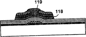
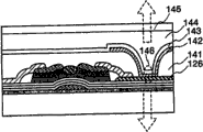
The thickness that dielectric film is preferably formed is 100nm or above to be used as channel protection film.In addition, dielectric film can form laminated construction.For example, lower floor can be made by the film that forms by CVD or sputtering method such as silicon nitride film; The upper strata can by the film that forms by the drop method for releasing, be made such as heat stable resin such as polyimides, acrylic acid or siloxanes.Perhaps, two-layerly all can be made by the film that forms by the drop method for releasing.Semiconductor film with dielectric film be preferably formed thickness 10nm or more than.
Usually, source area and drain region can form by etch away single conductive semiconductor film after forming the island shape semiconductor film.Therefore, before forming the island shape semiconductor film, need to provide the photoresist mask.Otherwise, according to the present invention, after source area and drain region formation, formed the dielectric film of corrugate pipe protection membrane interaction to cover the part as channel region, then form the island shape semiconductor film.Therefore, do not need to form the photoresist mask, can simplify procedures like this.As mentioned above; the invention provides and form the semiconductor element new tool; it combines and utilizes source electrode and drain electrode metal mask to form source area and drain region removing the method for single conductive semiconductor film, and is used to form the method that be exclusively used in raceway groove protection type of channel protection film to prevent that channel region from moving.According to above-mentioned embodiment of the present invention, can only utilize source electrode and drain electrode metal mask and need not make semiconductor element by any photoresist mask.
Before substrate release contained the composite material of the first electric conducting material, the part that can have at least gate electrode layer on substrate was carried out preprocessing process, for example forms titanium oxide (TiO
x) etc.Therefore, can improve substrate and conducting film, such as the viscosity between the gate electrode layer that forms by the drop method for releasing.
By forming thickness less than the semiconductor film of the tool dielectric film of other semiconductor film, the N-shaped impurity range can be divided into source area and drain region fully.By forming thickness at the semiconductor film of 10nm or above tool dielectric film, can obtain enough large channel mobility.
By forming thickness at 100nm or above dielectric film, can improve the function as channel protection film, and guarantee to prevent that channel region from damaging.Therefore, can provide the stabilization of semiconductor-element with high mobility.In addition, in order to obtain above-mentioned advantage, forming the double-layer structure that comprises the first dielectric film and the second dielectric film or three layers or above laminated construction, to consist of dielectric film very effective.
Summary of the invention
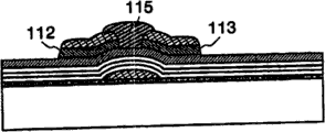
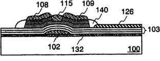
Explain the method for semiconductor element and this semiconductor element of manufacturing referring to figs. 1A to 1D.
With so-called photocatalysis material such as titanium or titanium oxide; Or heat stable resin such as polyimides, acrylic acid or siloxanes are formed on the part that substrate 100 has gate electrode layer at least.Here, formed oxidation titanium film 132.Perhaps, can carry out plasma treatment.This preliminary treatment is so that improve substrate 100 and contain viscosity between the conducting film that the composite material of electric conducting material makes by release.In the situation that form titanium oxide, can improve light transmittance.Titanium oxide can directly form, and also can form by the baking conducting film after forming titanium film.Except titanium or titanium oxide, can also form photocatalysis material such as strontium titanates (SrTiO
3), cadmium selenide (CdSe), potassium tantalate (KTaO
3), cadmium sulfide (CdS), zirconia (ZrO
2), niobium oxide (Nb
2O
5), zinc oxide (ZnO), iron oxide (Fe
2O
3) or tungsten oxide (WO
3).Carry out as much as possible above-mentioned preprocessing process and can improve viscosity between substrate and the conducting film.
The surface of substrate 100 is being carried out in the pretreated situation, discharging the composite material that contains the first electric conducting material at described preprocessing part and can form gate electrode layer 102.Here, gate electrode layer refers to by the layer that comprises that at least TFT gate electrode single or multiple lift electric conductor partly consists of.Form gate electrode layer by discharging described composite material; At 100 ℃ of lower dry described composite materials; Then the described composite material of baking 15 to 30 minutes in 200 to 350 ℃ nitrogenize or oxidizing atmosphere.Yet, be not only limited to above-mentioned condition.
As the first electric conducting material, can adopt according to the function of described conducting film various materials.Typical example has silver (Ag), copper (Cu), gold (Au), nickel (Ni), platinum (Pt), chromium (Cr), tin (Sn), palladium (Pd), iridium (Ir), rhodium (Rh), ruthenium (Ru), rhenium (Re), tungsten (W), aluminium (Al), tantalum (Ta), indium (In), tellurium (Te), molybdenum (Mo), cadmium (Cd), zinc (Zn), iron (Fe), titanium (Ti), silicon (Si), germanium (Ge), zirconium (Zr), barium (Ba), antimonial lead, contain antimony oxidation tin, the zinc oxide of fluoride-doped, carbon, graphite, vitreous carbon, lithium, beryllium, sodium, magnesium, potassium, calcium, scandium, manganese, zirconium, gallium, niobium, Na-K alloy, the magnesium copper mixture, magnesium silver mixture, the magnalium mixture, magnesium indium mixture, the aluminum aluminum oxide mixture, lithium aluminium mixture etc., perhaps particle and analog thereof such as silver halide, or dispersible nanoparticles; The gallium oxide zinc (GZO) that perhaps forms as the tin indium oxide (ITO) of conducting film, zinc oxide (ZnO), by the zinc oxide of mixing gallium, the tin indium oxide (IZO) that is formed by indium oxide and 2-20% zinc oxide, organo indium, titanium nitride etc.
Can contain silicon (Si) or silica (SiO in the above-mentioned electric conducting material
x), especially in the situation that above-mentioned material is used to form nesa coating.The electric conducting material (hereinafter being called ITSO) that for example, can use the ITO by oxide containing silicon to consist of.In addition, the layer that forms by stacked these electric conducting materials can be made the conducting film of expection.
The nozzle diameter that is used for the drop releasing device is set in 0.1 to 50 μ m (preferred 0.6 to 26 μ m), and burst size is set in 0.00001 to 50pl (preferred 0.0001 to 10pl).Burst size increases along with the increase of nozzle diameter.Object and nozzle liberation port are preferably closer to each other as much as possible, drop is transported to predetermined position.Distance between object and the liberation port preferably sets about 0.1 to 2mm.
Consider specific resistance value, the composite material that discharges from liberation port is preferably by with gold, silver or copper dissolution or be dispersed in the solvent and form.More preferably, can use low-resistance silver or copper.In the situation that use copper, preferably provide simultaneously barrier film as the measure of taking precautions against impurity.As solvent, can use the ester class, such as butyl acetate or ethyl acetate; Alcohols such as isopropyl alcohol or ethanol; Organic solvent such as methylethylketone or acetone; Etc..In the situation that use copper conductor as barrier film, can adopt the nitrogen substance with insulating properties or conductivity, such as silicon nitride, silicon oxynitride, aluminium nitride, titanium nitride or tantalum nitride (TaN) so that by drop release formation barrier film.
Be used for the composite material preferred viscosities of drop release at 300mPas or following dry also in order to successfully discharge from liberation port to prevent.The viscosity of composite material, surface tension etc. can maybe should be used for controlling according to solvent.For example, by ITO, ITSO, organo indium and organotin dissolving or be dispersed in the composite material viscosity that forms in the solvent 5 to 50mPas, by silver dissolving or be dispersed in the composite material viscosity that forms in the solvent 5 to 20mPas, by gold dissolve or be dispersed in the composite material viscosity that forms in the solvent 10 to 20mPas.
The particle diameter of electric conducting material is preferably as far as possible little, preferably at 0.1 μ m or following, preventing from blocking and making the high definition pattern, although this depends on diameter, pattern form of each nozzle etc.The particle diameter of the composite material that forms by known method such as electrolysis, spray-on process or wet reducing process is greatly about 0.5 to 10 μ m.In the situation that this composite material forms by gasification, the nano molecular of being protected by dispersant has the minute diameter of about 7nm.And this nano particle that the surface is covered by film forming agent can stably be dispersed in the solvent and can at room temperature not assemble, and this is just showing the character that is similar to liquid.Therefore, preferably use film forming agent.
Perhaps, gate electrode layer can contain by release the composite material formation of particle, and wherein the material of single conductivity-type is covered by another kind of electric conducting material.In this case, preferably has resilient coating between two electric conducting materials.By Ag cover the particle that Cu forms structure can for, between Cu and Ag, have Ni or NiB resilient coating.
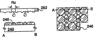
Contain in the process of composite material of electric conducting material by effectively utilizing the gas that is mixed with 10 to 30% division ratio oxygen in baking, can reduce to form the resistivity of the conducting film of gate electrode layer, and conducting film can be made thin and smooth film.To 8C, provided the general survey of conducting film state variation in the bake process referring to Fig. 8 A.The nano pulp 502 that Fig. 8 A has represented to contain electric conducting material such as Ag is released in state on the glass substrate 500 by nozzle 501.This nano pulp is dispersed or dissolved in the organic solvent by electric conducting material and forms.In addition, also contain dispersant or the thermosetting resin that is called adhesive in this organic solvent.This adhesive especially can prevent cracking and the inhomogeneous baking of nano pulp.By drying and bake process, the organic solvent vaporization, dispersant decomposes to be removed, and then nano pulp solidifies and shrinks because of adhesive simultaneously.Therefore, nano particle fuses to solidify this nano pulp each other.Simultaneously, the size of nano particle is grown up to thousands of nm from tens of nm, and the nano particle of adjacent growth merges and the formation metallic bond that connects together.On the other hand, the remaining organic principles of great majority (approximately 80 to 90%) are extruded outside the metallic bond.As a result, the conducting film 503 of containing metal chain and the film 504 (Fig. 8 B) that is consisted of by the organic principle of covering surfaces have been formed.In the situation that nitrogen and oxygen is when existing baking nano pulp 502, the film 504 that is made of organic principle can be removed by the carbon or the H-H reaction that comprise in the oxygen in the gas and the film 504 that is made of organic principle.In the situation that oxygen-free gas in the baking atmosphere, can be by removals (Fig. 8 C) such as oxygen plasma treatment by the film 504 that organic principle consists of.As mentioned above, removed according to following operation by the film 504 that organic principle consists of, namely in the situation that nitrogen and oxygen exist baking or drying nano slurry, and carry out oxygen plasma treatment.Therefore, the conducting film 503 of containing metal chain can be made into thin and smooth film, and reduces its resistivity.
In addition, contain the composite material of electric conducting material by the lower release of reducing pressure, the solvent evaporates in this composite material, thus shortened (the dry or baking) time of heat treatment subsequently.
Except dry and bake process, but effects on surface carries out smooth or smoothing processing.As the processing means, CMP (chemico-mechanical polishing) is arranged; Perhaps after forming the dielectric film with flatness, conducting film forms the method for smooth conducting film by etching.
As substrate, can adopt by insulator such as glass substrate the substrate that quartz substrate or aluminium oxide consist of; Have thermal endurance and can bear plastic of the treatment temperature in the reprocessing etc.In this case, can form end dielectric film and spread from substrate in order to prevent impurity, such as silica (SiO
x), silicon nitride (SiN
x), silicon oxynitride (SiO
xN
y) (x>y), silicon oxynitride (SiN
xO
y) (x>y) etc. (x, y=1,2...).Perhaps, can use metal such as stainless steel or have dielectric film such as the Semiconductor substrate of silica or silicon nitride.
Gate pole dielectric film 103 is formed on the gate electrode layer.The gate pole insulating barrier is made by the film of individual layer or lamination silicon nitride comprising, silica, silicon oxynitride or silicon oxynitride by film forming method such as plasma CVD, sputtering method etc.Here, silicon oxide film, silicon nitride film and silicon oxide film sequentially are formed on the substrate.Yet, be not limited in this structure, materials and methods.
In above-mentioned half unformed semiconductor, simplicity of explanation is SAS (half unformed silicon) once.SAS can decompose acquisition by the growth discharge of silicide gas.Can adopt SiH as typical silicide gas
4Also can adopt other silicide gas such as Si
2H
6, SiH
2Cl
2, SiHCl
3, SiCl
4, SiF
4Etc..Usually dilute silicide gas by the rare gas unit that is selected from hydrogen, hydrogen and helium, argon, krypton and neon with one or more and can easily make SAS.Dilution rate is preferably 10 to 1000 times scope.Certainly, the product for film forming forms by growth discharge decomposition under about reduced pressure of 0.1 to 133Pa.1MHz is to 120MHz, and preferred 13MHz can be for forming the growth discharge to the high-frequency current of 60MHz.The temperature of heated substrate is preferably 300 ℃ or following, more preferably at 100 to 200 ℃.
By in silicide gas, sneaking into carbide gas such as CH
4Or C
2H
6, or germanide gas such as GeH
4Or GeF
4Bandwidth can be controlled at 1.5 to 2.4eV, or 0.9 to 1.1eV.
When specially not mixing impurity with the control valence electron, SAS shows weak N-shaped conductivity.It is sneaked into semiconductor film easily along with oxygen and strengthens, because carry out under the electric current of growth discharge when being higher than the unformed semiconductor of formation.Therefore, in film forming simultaneously or afterwards, can control threshold value by in the first semiconductor film with channel formation region of TFT, mixing p-type impurity.As the impurity of giving p-type, usually can use boron.Can be with 1 to 1000ppm foreign gas such as B
2H
6Or BF
3Sneak in the silicide gas.When giving the impurity of p-type with the boron conduct, boron concentration can be 1 * 10
14To 6 * 10
16Individual atom/cm
3Form channel formation region by above-mentioned SAS, can obtain 1 to 10cm
2The electron field effect mobility of/Vsec.
Can obtain the crystal semiconductor film according to following steps, namely in the solution that contains catalyst such as nickel, process unformed semiconductor film; Under 500 to 750 ℃, heat the crystallization treatment process to obtain the crystal silicon semiconductor film; Carry out the laser crystallization process to improve degree of crystallinity.
Utilize disilane (Si
2H
6) and fluoridize germanium (GeF
4) unstrpped gas, directly form polycrystal semiconductor film by LPCVD (low pressure chemical vapor deposition) and can obtain the crystal semiconductor film.LPCVD can but be not limited only at Si
2H
6/ GeF
4=20/0.9 air-flow ratio, 400 to 500 ℃ of film-forming temperatures, carrier gas is to carry out under the condition of He or Ar.
N-shaped semiconductor film 105 is formed on the semiconductor film 104.As the N-shaped impurity element, can use arsenic (Ar) and phosphorus (P).In the situation that form the N-shaped semiconductor film, utilize plasma CVD method to pass through SiH
4, H
2And PH
3The growth discharge of (hydrogen phosphide) mist is decomposed can form N-shaped (n+) silicon fiml.Can be made into the semiconductor film that contains p-type impurity element such as boron (B) and replace N-shaped semiconductor film 105.
Can form source electrode 108 and drain electrode 109 by discharging the composite material that contains the second electric conducting material at N-shaped semiconductor film 105.Can be from above-mentioned to the structure of suitably selecting described the second electric conducting material, conductive particle the description of the first electric conducting material, release conditions, drying condition, baking condition etc.In addition, the first and second electric conducting materials and the first and second grain structures can identical or different (Figure 1A).
Although not shown, but can discharge the described composite material that contains the second electric conducting material to N-shaped semiconductor film 105 before, carry out preprocessing process, in order to improving the viscosity between N-shaped semiconductor film 105 and the source electrode 108, and the viscosity between N-shaped semiconductor film 105 and the drain electrode 109.Preprocessing process can carry out with being similar to the preprocess method that forms gate electrode 102.
Utilize source electrode 108 and drain electrode 109 as mask, with chlorine-containing gas such as Cl
2, BCl
3, SiCl
4Or CCl
4Fluoride gas such as CF
4, SF
6, NF
3Or CHF
3Or O
2As etching gas, form source area 112 and drain region 113 by plasma etching N-shaped semiconductor film 105.Yet, be not limited in this condition.Etching process can utilize atmospheric plasma to carry out.In this case, preferably use CF
4And O
2Mist as etching gas.When making N-shaped semiconductor film 105 and semiconductor film 104 with identical semiconductor, should be noted that etching speed and etching period because when etching N-shaped semiconductor film 105 also together etching semiconductor film 104.Yet forming thickness at the semiconductor film at channel formation region place is 5nm or higher, preferred 10nm or higher, more preferably in 50nm or the higher situation, though etching the part of semiconductor film 104, also can obtain enough TFT mobilities.
Carry out drop release by the channel region at semiconductor film 104 and formed dielectric film 115.Because the effect of dielectric film 115 corrugate pipe protection films, thereby can be by discharging heat stable resin such as siloxanes, or material such as acrylic acid, benzocyclobutene, polyamide, polyimides, benzimidazole or polyvinyl alcohol with elching resistant and insulating properties form.Preferred siloxanes and the polyimides of using.Excessive for preventing the channel region etching, can form thickness at 100nm or higher, preferred 200nm or higher dielectric film 115 (Figure 1B).Therefore, as shown in Figure 1B, dielectric film 115 can be made into the shape that is similar to buttress and is positioned at source electrode 108 and drain electrode 109 tops.
Then, utilize source electrode 108, drain electrode 109 and dielectric film 115 as mask, with chlorine-containing gas such as Cl
2, BCl
3, SiCl
4Or CCl
4Fluoride gas such as CF
4, SF
6, NF
3Or CHF
3Or O
2As etching gas, form island shape semiconductor film 118 by plasma etching semiconductor film 104.Yet, be not limited in this condition.Etching process can utilize atmospheric plasma to carry out.In this case, preferably use CF
4And O
2Mist as etching gas.And owing to being formed on the channel region 119 in the island shape semiconductor film 118 as the dielectric film 115 of channel protection film, channel region 119 can be owing to over etching damages in above-mentioned etching process.Therefore, need not just can produce the raceway groove protection type TFT (channel stopper type) (Fig. 1 C) with stability and high mobility by any photoresist mask.
The composite material that contains the 3rd electric conducting material by release forms source wiring 123 and drain electrode wiring 124 in order to contact with source electrode 108 and drain electrode 109, and by source wiring 123 is connected with pixel electrode 126 with drain electrode wiring 124, can provide the liquid crystal cell or the light-emitting component (be generally and adopt electroluminescent light-emitting component) that are consisted of by the layer that contains organic compound or inorganic compound.Therefore, can be made into active matrix liquid crystal display or thin display such as el light emitting device, can control by the semiconductor element of being made by said method respectively.Can be from above-mentioned to the structure of suitably selecting described the 3rd electric conducting material, conductive particle the description of the first electric conducting material, release conditions, drying condition, baking condition etc.In addition, the second and the 3rd electric conducting material and the second and the 3rd grain structure can be identical or different.Pixel electrode is preferably made (Fig. 1 D) by the drop method for releasing of ITO, ITSO, ZnO, GZO, IZO, organo indium, organotin etc.
Although not shown, can when forming source wiring 123, drain electrode wiring 124 and pixel electrode 126, carry out preprocessing process so that the viscosity between raising and the lower floor.Preprocessing process can be undertaken by being similar to the preprocess method that forms gate electrode layer 102.
As mentioned above, according to the present invention, after source area 112 and drain region 113 formation, thereby covered formation island shape semiconductor film as the part of channel region by the dielectric film 115 of corrugate pipe protection membrane interaction.Therefore, do not need the photoresist mask, can simplify working process like this.The invention provides and form the semiconductor element new tool; it combines and utilizes source electrode and drain electrode metal mask to form source area and drain region removing the method for single conductive semiconductor film, and is used to form the method that be exclusively used in raceway groove protection type of channel protection film to prevent that channel region from moving.According to above-mentioned structure, can only utilize source electrode and drain electrode metal mask and need not make semiconductor element by any photoresist mask.As a result, can simplify working process, and greatly reduce cost by economical with materials.Can realize that high flux ground makes the semiconductor element of high stability with low-cost high yield ground, with the minimizing production time, especially on the substrate large greater than 1 * 1m or its two or three times.
In semiconductor element according to the present invention, can improve the viscosity between substrate and the conducting film (such as the gate electrode layer that forms by the drop method for releasing etc.), pass through processing because have at least the part of gate electrode layer in the substrate, for example formed titanium oxide etc.
The semiconductor film part that has dielectric film by formation, thickness can be divided into the N-shaped impurity range source area and drain region undoubtedly less than other semiconductor film.And, having thickness more than 5nm by formation, the semiconductor film part of the semiconductor film that preferred 10nm is above can obtain enough large channel mobility.
In semiconductor element according to the present invention, the dielectric film 115 that is used as channel protection film is formed on the channel region 119, and therefore, channel region 119 can be owing to over etching damages in the etching process of semiconductor film 104.Thereby semiconductor element has stability and high mobility.By forming thickness at 100nm or above dielectric film, must improve dielectric film as the function of channel protection film in case the damage of channel region.Thereby, can obtain having the high stability semiconductor element of high mobility.For obtaining above-mentioned advantage, effectively make dielectric film form the double-decker that is formed by the first dielectric film and the second dielectric film, perhaps by three or the sandwich construction that forms of multilayer.
Brief Description Of Drawings
In the accompanying drawings:
Figure 1A is that expression is according to TFT process schematic representation of the present invention to 1D;
Fig. 2 A is that expression is according to TFT process schematic representation of the present invention to 2D;
Fig. 3 A is that expression is according to LCDs process schematic representation of the present invention to 3C;
Fig. 4 A and 4B are that expression is according to LCDs process schematic representation of the present invention;
Fig. 5 A is that expression is according to LCDs process schematic representation of the present invention to 5C;
Fig. 6 A is that expression is according to electroluminescence screen process schematic representation of the present invention to 6C;
Fig. 7 A is that expression is according to the schematic diagram of top of the present invention light-emitting device, end light-emitting device and dual light-emitting device to 7C;
Fig. 8 A is the method schematic diagram that expression is used to form oxidation titanium film to 8C;
Fig. 9 A represents an embodiment schematic diagram according to electric equipment of the present invention to 9C;
Figure 10 has represented the structure of drop delivery system;
Figure 11 A and 11B be expression to adopt spacing according to embodiment be the n nozzle doubly of pel spacing, the wiring schematic diagram that forms by the wiring of laying respectively even number line and odd-numbered line.
Figure 12 A is that expression discharges the pixel electrode schematic diagram that forms according to embodiment with a plurality of nozzles with different liberation port diameters to 12D;
Figure 13 A is that expression discharges the plane routing schematic diagram that forms according to embodiment with a plurality of nozzles with different liberation port diameters to 13C;
Figure 14 is that expression discharges the different line width wiring schematic diagrames that form according to embodiment with a plurality of nozzles with different liberation port diameters; And
Figure 15 A is that expression discharges the opening portion schematic diagram that forms, be filled with electric conducting material according to embodiment with a plurality of nozzles with different liberation port diameters to 15C;
Optimum implementation of the present invention
Embodiment 1
In embodiment 1, explained the situation of this substrate of preliminary treatment before substrate forms gate electrode layer.
First method can directly form oxidation titanium film 132, as shown in Figure 1A on substrate 100.By spin-coating method, liquid method for releasing, spraying process, sputtering method, CVD etc. oxidation titanium film 132 is spread all over is formed on the substrate.Afterwards, form gate electrode layer 102 by the drop method for releasing at oxidation titanium film 132.Thus, can improve viscosity between substrate 100 and the gate electrode layer 102 by between it, inserting oxidation titanium film 132.Form after the gate electrode layer 102, can stay or remove this gate electrode layer 102 oxidation titanium film 132 on every side by etching process.And etch processes is preferably under atmospheric pressure carried out.In addition, can form titanium film and replace forming oxidation titanium film.Here, gate electrode layer 102 can form by stacked Ag/Cu on oxidation titanium film.Perhaps, stacked Cu only on oxidation titanium film.
Second method optionally discharges the formation oxidation titanium film by drop.As the drop method for releasing, except ink-jet method, can also adopt silk screen printing or hectographic printing.Perhaps, can use collosol and gel.Afterwards, can on titanium oxide layer or titanium oxide layer inner surface, optionally form gate electrode layer by the drop method for releasing.In addition, can form titanium film and replace forming oxidation titanium film.
The third method spreads all over the formation titanium film by spin-coating method, drop method for releasing, sputtering method, CVD etc. at substrate; The composite material that contains electric conducting material that will be used to form gate electrode layer by the drop method for releasing optionally is formed at (Fig. 8 A) on the titanium film.Then, composite material is dry and baking.Simultaneously, this titanium film 505 of oxidation.Like this, around composite material, formed oxidation titanium film 506.Oxidation titanium film has good light transmission.For example, in the bottom-emission device, can effectively utilize oxidation titanium film with luminous from substrate, shown in Fig. 6 C and 7B.After substrate spreads all over the formation titanium film, before optionally release is used to form the composite material that contains electric conducting material of gate electrode layer, can form oxidation titanium film by heat treatment by spin-coating method, drop method for releasing, sputtering method, CVD etc.
Above-mentioned first in the third method, can replace forming titanium film and oxidation titanium film with so-called photocatalysis material, for example strontium titanates (SrTiO
3), cadmium selenide (CdSe), potassium tantalate (KTaO
3), cadmium sulfide (CdS), zirconia (ZrO
2), niobium oxide (Nb
2O
5), zinc oxide (ZnO), iron oxide (Fe
2O
3), tungsten oxide (WO
3) etc.Perhaps, for oxide, can use oxidized material (Zr, Nb, Zn, Fe, W etc.) before.
The 4th kind of method by forming heat stable resin at substrate, can improve viscosity between substrate and the electrode layer such as polyimides, acrylic acid, siloxanes etc.These materials can spread all over and are formed on the substrate or are formed with on the zone of gate electrode layer.Be formed on the substrate in the situation that this material spreads all over, can remove gate electrode layer residual film on every side by etching or ashing.
Lung biopsy can be tackified by the part that plasma treatment is formed with substrate and gate electrode layer.Preferred but be not limited under atmospheric pressure carry out plasma treatment.
Embodiment 2
In embodiment 2, explained the situation that forms the dielectric film of corrugate pipe protection membrane interaction by two-layer laminate.
As shown in Figure 1B, utilize source electrode 108 and drain electrode 109 as mask, form source area 112 and drain region 113 by etching N-shaped semiconductor film 105.Then, by methods such as CVD, sputtering methods silicon nitride film 133 is spread all over and be formed at whole surface (Fig. 2 A).On the zone of the channel region that is used as semiconductor film, form dielectric films 115 with silicon nitride film 133 by the drop method for releasing., dielectric film 115 be used for to remove the mask of silicon nitride film 133 because being not used as channel protection film, thereby by discharging heat stable resin such as siloxanes or having elching resistant and the composite material of the material of insulating properties such as acrylic acid, benzocyclobutene, polyamide, polyimides, benzimidazole or polyvinyl alcohol forms dielectric film 115.Preferred silica and the polyimides of using.Excessive for preventing the etching of raceway groove protection zone, the gross thickness that is preferably formed silicon nitride film 133 and dielectric film 115 100nm or more than, more preferably at 200nm or above (Fig. 2 B).
Thereby utilize dielectric film 115 to fall silicon nitride film 133 remaining dielectric films 115,134 as mask etching, they play respectively the effect of channel protection film.Dielectric film 134 undoubtedly is film formed by silicon nitride.Utilize chloride gas, Cl is arranged usually
2, BCl
3, SiCl
4, CCl
4Deng; Fluoride gas has CF usually
4, SF
6, NF
3, CHF
3Deng; Or O
2As etching gas, but by the plasma etching method silicon nitride film.Yet etching gas is not limited in this.Etch processes can adopt the atmos plasma method.
Double-deck channel protection film can improve the function as channel protection film, prevents that channel region from damaging, and the stabilization of semiconductor-element with high mobility is provided.Perhaps, can by stacked three or multilayer form channel protection film.Its bottom is not limited in silicon nitride film; Also can use the dielectric film that contains other silicon.This channel protection film can be by stacked can formation by film such as the dielectric film 115 of drop method for releasing film forming optionally.
Thereby utilize source electrode 108, drain electrode 109 and dielectric film 115,134 to form island shape semiconductor film 118 as mask etching semiconductor film 104.Be formed on the channel region 119 in this island shape semiconductor film 118 as the dielectric film 115 of channel protection film.Therefore, can prevent because the damage that the over etching in the above-mentioned etching process causes.Thereby, can any photoresist mask and produce ditch pipe protection (channel stopper) the type TFT (Fig. 2 C) with stability and height mobility.
The composite material that contains the 3rd electric conducting material by release forms source wiring 123 and drain electrode wiring 124, thereby contacts with source electrode 108 and drain electrode 109 in the mode described in the embodiment.And source wiring 123 or drain electrode wiring 124 are connected with pixel electrode.Then, by containing layer forming liquid crystal cell or the light-emitting component of organic compound or inorganic compound (be generally and utilize electroluminescent light-emitting component).Therefore, can obtain thin display such as active array liquid crystal display or active matrix electroluminescent display, they can control by the semiconductor element of being made by said process (Fig. 2 D) respectively.
Embodiment 3
In embodiment 3, explained by drop to discharge the method that combines to form conducting film with galvanoplastic.
At first, discharge the composite material that formation contains Ag by drop.In this case, for a few to tens of μ m than the thick wiring of the wide middle formation of narrow row, need to repeatedly discharge Ag.Perhaps, can be immersed in by the substrate that will have Ag in the electroplating solution that contains Cu, perhaps directly this electroplating solution being sprayed on increases line width on the substrate.Discharge the composite material that forms by drop and especially have many scramblings, therefore can easily electroplate.In addition, because Ag is expensive, Cu is so that cost in plating.The electric conducting material that method by this embodiment is used to form wiring is not limited in mentioned kind.
After plating Cu, by forming resilient coating, this has conducting film surface of scrambling to come planarization process such as NiB etc.Then, be preferably formed the gate pole dielectric film.
Embodiment 4
In embodiment 4, explained according to the present invention for the manufacture of the method for thin film transistor,Bao Mojingtiguan screen board with reference to figure 3A to 5C.
First method, be released in made in accordance with the present invention by drop and optionally form planar film 151 on the TFT, and be released in by drop and form respectively source wiring and the drain electrode wiring 152 that is connected with drain electrode with the source electrode on the zone that does not form planar film 151, as shown in Figure 3A.In addition, the source wiring or the drain electrode wiring that link to each other with pixel TFT 654 can be used as pixel electrode, as shown in Figure 3A.Certainly, can form respectively pixel electrode to connect source wiring or drain electrode wiring.Source electrode, drain electrode, source wiring and drain electrode wiring can be made by identical or different electric conducting material.
The method does not adopt contact hole to be formed at design in the planar film.As if yet it has formed contact hole in appearance.Therefore, the method is called as loose contact.As planar film, be preferably formed organic resin, such as acrylic acid, polyimides or polyamide, perhaps have Si-O key and Si-CH
xThe dielectric film of valency, it is by making as raw-material material based on siloxanes.
Afterwards, liquid crystal layer 154 is inserted between TFT substrate and the relative substrate.These materials are bonded together by sealant 159.Formed cylinder spacer block 158 on the TFT substrate.This cylinder spacer block 158 can form along the contact hole recess that is formed on the pixel electrode.The height that cylinder spacer block 158 is preferably formed is at 3 to 10 μ m, although this depends on liquid crystal material.The recess of contact portion is equivalent to contact hole.By forming the distortion that can prevent liquid crystal aligning along the spacer block of this recess.
Alignment films 153 is formed on the TFT substrate.Then carry out friction treatment.Then, form nesa coating 156 and alignment films 157 at relative substrate 155.Afterwards, by sealant with the TFT substrate and relatively substrate attaching together in order between it, to inject liquid crystal.Like this, formed liquid crystal layer 154.Thereby, finished active matrix liquid crystal display.In addition, liquid crystal layer 154 can form by dropwise adding liquid crystal.Especially, this to make under the case of liquid crystal displays greater than the large active array substrate of 1m be unusual effective method adopting.
And, alignment films 153,157, and cylinder spacer block 158 can optionally form by the drop method for releasing.Especially, this is unusual effective method adopting in the situation of making liquid crystal display greater than the large active array substrate of 1m.
The following describes end 652.As shown in Fig. 1 or similar figure, the gate pole dielectric film is stayed in the zone except the TFT element.Therefore, need to be used for connect the wiring 171 that forms simultaneously with gate electrode layer and the contact hole of FPC 628 (flexible printed circuit).Here, the zone that will form contact hole is covered by the conductor 172 that forms by the drop method for releasing on every side, has formed contact hole with this conductor as mask.Discharge with the identical or different conductor 173 of conductor 172 with filling contact hole by the drop method for releasing.Like this, conductor 172 and 173 can be formed on the gate pole dielectric film.According to known method by anisotropic conductive film 627 with conductor 172,173 and FPC 628 bonding with termination electrode 626, wiring 171 can be linked to each other with FPC 628.Termination electrode 626 preferably forms by nesa coating.
Contact hole in the FPC part can be opened in the process of making TFT.Perhaps, can open contact hole by when forming source wiring and drain electrode wiring, forming conductor 172 or 173.An advantage of drop method for releasing is, composite material can optionally be released in predetermined site.A drop release process preferably plays the effect of a plurality of conventional operations.
By said process, the thin film transistor,Bao Mojingtiguan screen board of TFT constructed in accordance is adopted in complete manufacturing.TFT can form by the method described in embodiment or the embodiment.Here, a transistor has a pixel.Yet, also can have a pixel by two or more transistor.The polarity of TFT can be N-shaped or p-type.TFT can be made into the CMOS structure that is made of N-shaped TFT and p-type TFT.It is similar to the situation of drive circuit TFT 653.In the situation that form the CMOS structure, the wiring that is used for each TFT of connection can after optionally form above-mentioned planar film, discharge the composite material that contains electric conducting material by drop in opening portion and form.
Second method, shown in Fig. 3 B, tubular conductor 160 (be also referred to as post, plug etc.) discharges on the source electrode and drain electrode that is formed at TFT made in accordance with the present invention by drop.As the electric conducting material that forms cylinder, can use to be similar to the material that forms above-mentioned gate electrode layer or analog.Planar film 150 is formed on the tubular conductor 160 by modes such as drop releases.As planar film, by optionally drop release, be preferably formed organic resin, such as acrylic acid, polyimides or polyamide, perhaps have Si-O key and Si-CH
xThe dielectric film of valency, it is by making as raw-material material based on siloxanes.
In the situation that planar film is formed on the cylinder, but the surface of etching planar film and cylinder is to obtain to have the cylinder of plane surface, shown in Fig. 3 C.The source wiring and the drain electrode wiring 152 that are used for connection source electrode and drain electrode are formed at planar film by drop release.The source wiring and the drain electrode wiring 152 that link to each other with pixel TFT 654 can be used as pixel electrode, shown in Fig. 3 C.Undoubtedly, pixel electrode can make respectively to connect source wiring or drain electrode wiring.In addition, source electrode, drain electrode, cylinder, source wiring and drain electrode wiring are made by identical or different electric conducting material.
Afterwards, the forming process of liquid crystal cell is identical with first method.Contact hole in the FPC part can be opened in the process of making TFT.Perhaps, can open contact hole by when forming cylinder, source wiring and drain electrode wiring, forming conductor 172 or 173.
The third method, as shown in Fig. 4 A, the tubular insulator (hereinafter being called post insulator 161) that has liquid flow (liquid-shedding) character with respect to the material of planar film 151 is formed on the source electrode and drain electrode of making by the drop method for releasing according to the present invention; Planar film 151 be formed at post insulator 161 around.As the material of post insulator, can use water-soluble organic resin as at CF
4Processed the PVA (polyvinyl alcohol) with liquid flow character in the plasma.As planar film, preferably optionally form organic resin by the drop method for releasing, such as acrylic acid, polyimides or polyamide, perhaps by making, have Si-O key and Si-CH as raw-material material based on siloxanes
xThe dielectric film of valency.After forming planar film 151 around the post insulator 161, post insulator 161 can easily be removed by methods such as washing, etchings.In the situation that remove by etching, preferably carry out anisotropic etching in case contact hole is in an inverted cone.And, because post insulator such as PVA have insulating properties, even having stayed the side-walls of contact hole, the SI semi-insulation body can not cause any problem yet.
Afterwards, being connected source wiring that contact hole is connected and drain electrode wiring 152 with drain electrode with the source electrode discharges by drop and is formed on the planar film.The source wiring or the drain electrode wiring 152 that are connected with pixel TFT 654 can be used as pixel electrode, as shown in Fig. 4 B.Undoubtedly, pixel electrode can make respectively to connect source wiring or drain electrode wiring.In addition, source electrode, drain electrode, cylinder, source wiring and drain electrode wiring are made by identical or different electric conducting material.Form in the situation of back taper the contact hole in can forming with filling source wiring and drain electrode wiring by the stacked composite material that contains electric conducting material of drop method for releasing in the process of contact hole owing to the above-mentioned post insulator of removal.
Identical in the process that forms liquid crystal and the first method.Contact hole in the FPC part can be opened in the process of making TFT.Perhaps, can open contact hole by when forming source wiring and drain electrode wiring, forming conductor 172 or 173.
The 4th kind of method as shown in Fig. 5 A, is formed on the TFT source electrode and drain electrode of making by methods such as drop release, spin coating, splashes according to the present invention with respect to the liquid flow material 162 of the material of planar film 151; The mask 163 of making by PVA, polyimides etc. is formed in the zone that will form contact hole; Utilize the removal liquid flow materials 162 such as PVA; Planar film 151 be formed at remaining liquid flow material 162 around.Material as forming liquid flow material 162 can use fluoro silane coupler such as FAS (silicon fluoride) or analog.Optionally form mask 163 such as PVA, polyimides etc. by the drop method for releasing.Liquid flow material 162 can be removed by oxygen ashing or atmospheric pressure plasma.In addition, the mask 163 that PVA makes also can easily be removed by washing, and the mask 163 that is perhaps formed by polyimides can easily be removed by stripper N300.
Stay under the state in the zone that will form contact hole (Fig. 5 B) at liquid flow material 162, can discharge by drop, the method such as spin coating makes planar film 151.Because liquid flow material 162 is stayed in the zone that will form contact hole, just do not form planar film on it.And contact hole can't form back taper.As planar film, preferably optionally form organic resin by the drop method for releasing, such as acrylic acid, polyimides or polyamide, perhaps by making, have Si-O key and Si-CH as raw-material material based on siloxanes
xThe dielectric film of valency.After planar film 151 formed, liquid flow material 162 can be removed by oxygen ashing or atmospheric pressure force method.
Afterwards, being connected source wiring that contact hole is connected and drain electrode wiring 152 with drain electrode with the source electrode discharges by drop and is formed on the planar film.The source wiring or the drain electrode wiring 152 that are connected with pixel TFT 654 can be used as pixel electrode, as shown in Fig. 5 C.Undoubtedly, pixel electrode can make respectively to connect source wiring or drain electrode wiring.In addition, source electrode, drain electrode, source wiring and drain electrode wiring are made by identical or different electric conducting material.
Identical in the process that forms liquid crystal and the first method.Contact hole in the FPC part can be opened in the process of making TFT.Perhaps, can open contact hole by when forming source wiring and drain electrode wiring, forming wire 172 or 173.
In above-mentioned first to the 4th kind of method, Fig. 3 A is not shown in the 5C, can insert TiOx film etc. between substrate and gate electrode layer by preprocessing process and improve viscosity between them.Preprocessing process can be in the situation that form source wiring, drain electrode wiring, cylinder, pixel electrode, conductor 172, conductor 173 etc. and carry out.As preprocessing process, can adopt the processing described in embodiment and the embodiment.
In addition, preferably prevent the passivating film (not shown) that impurity spreads at TFT at source electrode and drain electrode formation.Passivating film can be by silicon nitride, silica, silicon oxynitride, silicon oxynitride, aluminium oxynitride; Or other insulating material for example aluminium oxide, diamond-like-carbon (DLC) or nitrogenous carbon (CN), form by film forming method such as plasma CVD or splash method.This material can be identical with the material that is used to form channel protection film.Perhaps, these materials can be laminated construction.In addition, passivating film can be formed by the drop method for releasing by the composite material that contains insulating material particle.
Pixel electrode can not provide planar film and indirectly is formed on the substrate, and can form the alignment films (not shown) thereon.In this case, TFT is preferably covered by insulation epiphragma or passivating film.
Embodiment 5
In embodiment 5, explained according to the present invention for the manufacture of the method for active matrix electroluminescence screen board with reference to figure 6A to 6C.
At first, as shown in Figure 6A, make TFT according to the said method described in embodiment and the embodiment.Then, will be formed at place, the semi-conductive at least side of island type be used to the insulator 140 that improves stepcoverage (being also referred to as the limit covers).Form source wiring 123 and drain electrode wiring 124, contact with source electrode 108 and the drain electrode 109 of TFT respectively.The source electrode links to each other with pixel electrode 126 (in general being hole injecting electrode (anode)) with drain electrode.In this case, wiring can form glossily with good coverage rate, covers because have the limit under the wiring layer.Therefore, can prevent fracture (Fig. 6 B).
In addition, can form the pixel electrode 126 with stromatolithic structure.For example, adopt the ITSO of stromatolithic structure, wherein the silica concentration of TFT side ITSO preferably sets into low concentration (1 to 6 atom %), and the silica concentration of light-emitting component side ITSO preferably sets into high concentration (7 to 15 atom %).The surface of pixel electrode 126 can be by the CMP leveling or by the polishing of polyvinyl alcohol porous body.After the CMP polishing, the surface of pixel electrode 126 can or be processed in oxygen gas plasma with the ultraviolet ray irradiation.
After etching formation pixel electrode 126, indium, tin, indium oxide or tin oxide discharge from the conductive layer inside that forms pixel electrode 126, and described conductive layer cleans (water washing) process, ultraviolet irradiation process etc. and forms by photoresist stripping process, water.Therefore, silicon, silica, silicon nitride etc. are deposited in the layer of conductive layer surface or near surface, thereby form by the barrier layer of deposition materials as main component.Can specially form the barrier layer by silicon, silica, silicon nitride etc. by methods such as vapour deposition, splashes.This barrier layer can increase the work function of hole injecting electrode and improve the hole injection.
The top of TFT, wiring and pixel electrode can be covered by the dike (bank) that the drop method for releasing optionally forms.As dike 141, the preferred employing has Si-O key and Si-CH
xValency, by organic resin such as acrylic acid, polyimides or polyamide, perhaps as the raw-material dielectric film of making based on the material of siloxanes.
Then, formation contains the layer of organic compound (be also referred to as electroluminescence layer, hereinafter be called " organic compound layer 142 "), in order to contact with the pixel electrode 126 of dike 141 opening parts.This organic compound layer 142 can be made of individual layer or lamination.For example, this organic compound layer 142 can have structure: 1) anode/hole injection layer/hole transmission layer/luminescent layer/electron transfer layer/negative electrode; 2) anode/hole injection layer/luminescent layer/electron transfer layer/negative electrode; 3) anode/hole injection layer/hole transmission layer/luminescent layer/electron transfer layer/electron injecting layer/negative electrode; 4) anode/hole injection layer/hole transmission layer/luminescent layer/hole blocking layer/electron transfer layer/negative electrode; 5) anode/hole injection layer/hole transmission layer/luminescent layer/hole blocking layer/electron transfer layer/electron injecting layer/negative electrode, etc.
Form electron injection electrode 143 (negative electrode) to cover organic compound layer 142.Electron injection electrode 143 can be made by the known material with low work function, such as Ca, Al, CaF, MgAg or AlLi.Can form light-emitting component 146 by opening part overlaid pixel electrode 126, organic compound layer 142 and electron injection electrode 143 at dike 141.Passivating film 144 is formed at (Fig. 6 C) on the electron injection electrode 143.
Above-mentioned light-emitting component consists of by being inserted in the laminated type luminescent layer that contains organic compound or inorganic compound between the electrode pair, and it has respectively different carrier transport properties.The hole is from the electrode injection electronics from another electrode injection.This light-emitting component has utilized from the hole of electrode injection with from the electronics of another electrode injection and has recombinated with excited emission centers each other, and when excited molecule is got back to ground state with the phenomenon of the form emittance of light.The work function size (from metal or semi-conductive surface attract electronics required least energy outside this surface) that forms the material of electrode is that the hole of this luminescent layer is injected and the index of electronic injection character.The electrode that is used for injected hole preferably has large work function, and preferably has little work function for the electrode that injects electronics.
Preferably form wavelength plate, polarization plates and anti-reflective film at relative substrate 145.As wavelength plate, can sequentially form λ/4 and λ/2 to set slow axis.
For finishing the state shown in Fig. 6 C, preferably pack this light-emitting component in case be exposed in the air by the air-tightness diaphragm (multilayer film, ultraviolet-curing resin film etc.) or the cladding material that are difficult for gas leakage.
Embodiment 6
In embodiment 5, explained end light-emitting device constructed in accordance, shown in Fig. 6 C.Among the embodiment 6, explained the dual light-emitting device shown in the top light-emitting device shown in Fig. 7 A and Fig. 7 C, it is constructed in accordance respectively.
Dual light-emitting device at first is described.As the material of hole injecting electrode, can adopt such as nesa coating used among the embodiment 5, such as ITO, ITSO, ZnO, IZO or GZO.In the situation that with ITSO as pixel electrode 126, can overlappingly contain the multilayer ITSO layer of variable concentrations silica.Preferably, end ITSO layer (being positioned at source wiring or drain electrode wiring side) preferably has the silica of low concentration, the silica that top ITSO layer (being positioned at the luminescent layer side) preferably has high concentration.Therefore, the connection between pixel electrode 126 and the TFT can keep low resistance, and can improve to the efficient of electroluminescence layer injected hole.Certainly, can make pixel electrode by stacked other material and ITSO (for example sequential cascade ITO layer and ITSO layer).Perhaps, can form the lamination that is consisted of by other material.
As electron injection electrode 143, but used thickness 1 to the thin aluminum film of 10nm, the aluminium film that namely contains by trace Li or analog sees through the light that produces in the luminescent layer.Like this, the top and bottom surface can be obtained and the dual light-emitting device of the light that produces in the light-emitting component (Fig. 7 C) can both be sent.
In 7C, Reference numeral 141 and 142 represents dikes at Fig. 7 A; 142 is organic compound layer; 144 is passivating film; 145 is relative substrate; And 146 be light-emitting component.
Then, referring to Fig. 7 A explanation top light-emitting device.In general, light can obtain by following steps from the top light-emitting device that the substrate offside sends (top): illuminated electron injection electrode 143 exchanges of pixel electrode 126 and the end as hole injecting electrode shown in Fig. 7 B contain the layer reverse stack of organic compound with the polarity of upset TFT (adopting N-shaped TFT).At electrode and containing in the layer reverse stack situation as shown in Figure 7A of organic compound, the stromatolithic structure of the luminescent oxygen compound conductive layer formation by containing the variable concentrations silica is made pixel electrode 126 and can be obtained having the luminous efficiency of improvement and the high stability light-emitting device of low-power consumption.As electron injection electrode 143, can adopt metal electrode or analog with reflective.
Embodiment 7
Adopted the electrical equipment example of the electroluminescence screen board described in the liquid crystal display panel described in the embodiment 4 or the embodiment 5,6 to have, radiovisor, Portable book (e-book), mobile phone, such as Fig. 9 A to as shown in the 9C.
Fig. 9 A has represented radiovisor, wherein adopts the display module 2002 of liquid crystal or electroluminescent cell to be arranged in the shell 2001; Recipient 2005 receives composite television broadcasting, thereby and is connected to wireless or wire net unidirectional (reflector is to receiver) and two-way (between reflector and the receiver, perhaps between the receiver) exchange message by modulator-demodulator 2004.This radiovisor can by be located in the shell or Digiplex 2006 in switch control.Remote controller 2006 can have display part 2007 in order to demonstration information.
Except main screen 2003, this radiovisor can also have by the second display module make, above be used for the small screen 2008 of indicated channel or volume.Main screen 2003 can be made by the electroluminescence display module with good visual angle.The small screen can be by showing that the LCD MODULE of image makes with low-power consumption.In order preferentially to reduce power consumption, main screen 2003 can be made by LCD MODULE, and the small screen can be made by the electroluminescence display module that can make the small screen flicker.
Fig. 9 B has shown the Portable book (e-book) that is made of main body 3101, display part 3102,3103, storage medium 3104, console switch 3105, antenna 3106 etc.
Fig. 9 C has represented a kind of mobile phone.Reference numeral 3001 expression display screens, 3002 expression guidance panels.Display screen 3001 and guidance panel 3002 are connected to each other by coupling part 3003.3003 places, coupling part can be changed arbitrarily by the angle θ between the face that has operation keys 3006 on the face that has display part 3004 on the display screen 3001 and the guidance panel 3002.This mobile phone also comprises voice output part 3005, operation keys 3006, mains switch 3007, Speech input part 3008, antenna 3009.
Embodiment 8
Preferably make by the drop delivery system shown in Figure 10 according to semiconductor element of the present invention.At first, carry out circuit design, such as CAD, CAM, CAE etc., and pass through the predetermined design that circuit design insturment 800 is determined films and alignment mark.
The Thinfilm pattern data 801 input computers 802 that will comprise the design of the film that designs and alignment mark are in order to control the drop releasing device by information network such as storage medium or LAN (local area network (LAN)).Data 801 according to Thinfilm pattern, selection has the nozzle of the liberation port of optimum diameter other nozzle (being used for from the device of small end opening spraying liquid or gas) of drop releasing device 803, wherein store the composite material of film forming material, perhaps it is connecting the tank that stores this composite material; Then, determine drop releasing device 803 scanning patterns (mobile route).In the situation that pre-determined optimum nozzle, only need to determine the mobile route of nozzle.
Afterwards, the drop releasing tool 803 of controlling by controller 808 discharges composite material 818 according to predetermined scanning pattern, and forms the Thinfilm pattern 809 of expection.By the diameter of selective liberation mouth can be suitable the control burst size.Yet slight variation can occur with some conditions in burst size, for example the temperature of the atmosphere of the rate of release of the distance between the translational speed of liberation port, liberation port and the substrate, composite material, Free up Memory, Free up Memory or humidity.Therefore, need these conditions of control.Preferably in advance by experiment or estimation determine optimum condition, and preferably with these results to every kind of composite material building database.
As having of Thinfilm pattern data, be used for circuit diagram or the analog of the active matrix TFT substrate of liquid crystal display for example or electroluminescent display.Figure 10 has represented to be used for the cycling circuit figure schematic diagram of the conducting film of this active matrix TFT substrate.The said gate pole wiring of Reference numeral 821 expressions; The 822nd, source signal line (the second wiring); The 823rd, pixel electrode, or hole injecting electrode or electron injection electrode; The 820th, substrate; And 824 are alignment marks.Certainly, Thinfilm pattern 809 is corresponding to the wiring of the gate pole in the Thinfilm pattern information 821.
In addition, drop releasing tool 803 can have but be not limited only to nozzle 810,811 and 812 integrated combination.Each nozzle has a plurality of liberation ports 813,814 and 815.Said film pattern 809 is by selecting predetermined liberation port 813 to form in nozzle 810.
Drop releasing tool 803 preferably has the nozzle of a plurality of different liberation ports, burst size or injector spacing, in order to can produce the Thinfilm pattern with various line width and improve the production time.Distance between the liberation port is preferably more narrow better.In addition, drop releasing tool 803 preferably has the nozzle of length more than 1m, in order to discharge on high flux ground on 1 * 1m or above or its two or three times of large substrate in size.Drop releasing tool 803 can be retractile in order to freely control distance between the liberation port.For obtaining high-resolution, namely depict level and smooth pattern, can angled nozzle or shower nozzle.Thereby, can chart such as the rectangular area in the bulk zone.
A shower nozzle can parallelly have the nozzle of the shower nozzle of different spacing.In this case, the diameter of liberation port can be identical or different.In the situation of the drop releasing device that adopts as mentioned above a plurality of nozzles, need to provide not nozzle holding fix in use.This wait position can have air feed instrument and porous nozzle the atmosphere in the holding fix is replaced to the atmosphere identical with composite material solvent gas.Therefore, can prevent to a certain extent drying.And, can have the cleaning unit of supplying with cleaned air or analog to reduce the dust in the working position.
In the situation that the distance between the liberation port can not narrow down owing to nozzle 803 specifications, injector spacing can be designed to the integral multiple of pixel in the display.Like this, as shown in Figure 11 A and 11B, composite material can be released on the substrate 804 by moving substrate 804.As imaging tool 805, can adopt the camera C CD (electric coupling device) that utilizes semiconductor element strong and weak light to be converted to the signal of telecommunication.
Said method be for by the stationary substrate of drop releasing device 803 on the predetermined path scan table 816 to form Thinfilm pattern 809.On the other hand, can form Thinfilm pattern 809 in the step, that is, fixedly drop releasing device 803, platform 809 is transmitted in XY θ direction along the paths that the data 801 of Thinfilm pattern are determined.In the situation that drop releasing device 803 has a plurality of nozzles, need to determine to have the nozzle of optimum diameter liberation port, it stores the composite material that comprises film forming material, is perhaps connecting the tank that is used for storing this composite material.
In addition, can use a plurality of nozzles with unnecessary amount.For example, when nozzle 812 (or 811) when at first discharging composite material, release conditions can be controlled so that nozzle 810 discharges composite material simultaneously with nozzle 812 (or 811).Therefore, even if for example liberation port obstruction of some problem appears in front nozzle, composite material also can discharge from rear nozzle 810, and it can prevent wiring interruption or Similar Problems at least.
Said method has only utilized a kind of predetermined liberation port of nozzle 810 to form Thinfilm pattern 809.Perhaps such as Figure 12 A to as shown in the 15C, according to the line width that will form or film thickness, can discharge composite material with a plurality of nozzles.
Figure 12 A has represented to 13C to 12D and Figure 13 A, for example, forms pixel electrode pattern 244 at substrate 240.Here, used by the big or small R of difference
1, R
2And R
3(R
1>R
2>R
3) the drop releasing tool 241 that consists of of three nozzles 251 to 253.At first, utilize the nozzle 251 with maximum gauge liberation port to discharge composite material 245 (Figure 12 B or 13A).Then, can not chart or optionally discharge composite material 246 (Figure 12 C or 13B) by the position with scrambling that the maximum gauge liberation port causes with the diameter of the liberation port nozzle 252 less than nozzle 251.Afterwards, the leveling patterned surfaces uses nozzle 253 selectivity with minimum diameter liberation port to discharge composite material 247 (Figure 12 D or 13C) on demand.The method can be effectively for the manufacture of larger conductor such as pixel electrode.The method can be made the plane pattern that does not have degree of irregularity.
Figure 14 has represented that wiring pattern 248 is formed at the state on the substrate 240.As the drop releasing device, can use said nozzle 251 to 253.Because the amount of each drop 261 to 263 that discharges from these nozzles is different, is easy to make the pattern with different line width, as shown in Figure 14.
Figure 15 A has represented to form with filling opening part 213 by sequentially discharging composite material to 15C, for example the method for conducting film.Reference numeral 210 expression substrates; 211 is semiconductor or conductor; And 212 be insulator.Insulator 212 has opening 213.Discharge composite material by the drop releasing tool that comprises a plurality of nozzles 251 to 253, described nozzle is arranged to multirow, and liberation port is arranged in the coaxial direction of above-mentioned each row.It is large that opening diameter becomes from bottom to top.At first, be R by the liberation port diameter
3Nozzle 253 composite material is filled in the opening 213 until bottom (Figure 15 A).Then, be R by the liberation port diameter
2Nozzle 252 composite material is filled in the opening 213 until middle part (Figure 15 B).Following, is R by the liberation port diameter again
1 Nozzle 251 composite material is filled in the opening 213 until top (Figure 15 C).According to the method, can form the plane conductive layer by discharging composite material filling opening.Like this, the insulator 212 that has a high-aspect-ratio opening can have plane routing in the situation that do not produce the space.
As mentioned above, the drop delivery system that is used to form film or wiring comprises the input tool for the data of input expression Thinfilm pattern; Be used for setting the nozzle mobile route contains the composite material of film forming material with release setting means; For detection of the imaging tool that is formed at the alignment mark on the substrate; And the control tool that is used for the Control Nozzle mobile route.Therefore, in the drop dispose procedure, need accurate Control Nozzle or substrate mobile route.By the program of controlling the composite material release conditions is installed in order to control the drop delivery system in computer, accurately controlled condition, for example heating-up temperature of the translational speed of substrate or nozzle, burst size, jet length, jet velocity, release atmosphere, release temperature, release humidity, substrate etc.
Therefore, can be in film or the wiring that predetermined position is accurate with the shorter production time and preset width, thickness and shape are made in high flux ground.And, can improve production output, comprising: utilize the thread semiconductor element of film or cloth, such as TFT; The light-emitting device that utilizes semiconductor element to make is such as liquid crystal display or display of organic electroluminescence; LSI or analog.Especially, according to the present invention, can form film or wiring at any position, and the width of controlled pattern, thickness and shape.Therefore, can be low-cost and high yield ground make big or small at 1 * 1m or above or its two or three times large large-scale semiconductor substrate.
Industrial applicibility
According to the present invention, form source area and drain region by said method, the dielectric film that is used as channel protection film as the part of channel region covers, thus formation island shape semiconductor film.Therefore, owing to do not need the photoresist mask, can process simplification.As mentioned above; an aspect of of the present present invention is to provide the new tool that forms semiconductor element; it combines and utilizes source electrode and drain electrode metal mask to remove the method for single conductive semiconductor film, and is used to form the method that be exclusively used in raceway groove protection type of channel protection film to prevent that channel region from moving.Can be only need not make semiconductor element by any photoresist mask with source electrode and drain electrode metal mask according to above-mentioned structure.Therefore, semiconductor element and the method for making this semiconductor element are applicable to best structure is provided and have the technique that felicity condition is effectively made by the drop method for releasing.
Claims (25)
1. electroluminescent display, described electroluminescent display comprises:
Be formed at the whole lip-deep layer that comprises titanium oxide of substrate;
Be formed at described comprise titanium oxide the layer on gate electrode layer;
Contact the door-plate dielectric film that forms with the top surface of gate electrode layer top surface and the layer that comprises titanium oxide;
Be formed at the semiconductor film on the described gate pole dielectric film;
Be formed at a pair of N-shaped impurity range on the described semiconductor film;
Be inserted in this between the N-shaped impurity range and be formed at dielectric film on the described semiconductor film part;
Be formed at this to the conductive layer on the N-shaped impurity range; With
The pixel electrode that is electrically connected with described conductive layer;
Wherein said dielectric film contacts with described conductive layer;
Wherein said dielectric film is formed has laminated construction; And
Wherein said gate electrode layer is formed by nesa coating.
2. electroluminescent display, described electroluminescent display comprises:
Be formed at the whole lip-deep layer that comprises titanium oxide of substrate;
Be formed at described comprise titanium oxide the layer on gate electrode layer;
Contact the gate pole dielectric film that forms with the top surface of gate electrode layer top surface and the layer that comprises titanium oxide;
Be formed at the semiconductor film on the described gate pole dielectric film;
Be formed at a pair of N-shaped impurity range on the described semiconductor film;
Be inserted in this between the N-shaped impurity range and the thickness that is formed on the described semiconductor film part be 100nm or larger dielectric film;
Be formed at this to the conductive layer on the N-shaped impurity range; With
The pixel electrode that is electrically connected with described conductive layer;
Wherein said dielectric film contacts with described conductive layer;
Wherein said dielectric film is formed has laminated construction; And
Wherein said gate electrode layer is formed by nesa coating.
3. electroluminescent display, described electroluminescent display comprises:
Be formed at the whole lip-deep layer that comprises titanium oxide of substrate;
Be formed at described comprise titanium oxide the layer on gate electrode layer;
Contact the gate pole dielectric film that forms with the top surface of gate electrode layer top surface and the layer that comprises titanium oxide;
Be formed at the semiconductor film on the described gate pole dielectric film;
Be formed at a pair of N-shaped impurity range on the described semiconductor film;
Be inserted in this between the N-shaped impurity range and be formed at dielectric film on the described semiconductor film part;
Be formed at this to the conductive layer on the N-shaped impurity range; With
The pixel electrode that is electrically connected with described conductive layer;
Be formed with wherein in the described semiconductor film of dielectric film as the thickness of the part of the channel region thickness less than other semiconductor film, and above the thickness that is formed with in the described semiconductor film of dielectric film as the part of channel region be 10nm or larger;
Wherein said dielectric film contacts with described conductive layer;
Wherein said dielectric film is formed has laminated construction; And
Wherein said gate electrode layer is formed by nesa coating.
4. each described electroluminescent display in 3 according to claim 1, wherein said dielectric film comprises at least a material that is selected from following group: polyimides, acrylic acid and have the silica bonding and form skeleton and comprise at least hydrogen substituting group or at least a substituent material that is selected from fluoride, alkyl and aryl.
5. each described electroluminescent display in 3 according to claim 1, wherein said electroluminescent display are included in and are selected from radiovisor, e-book and mobile phone at least a.
6. method of making electroluminescent display comprises:
Form gate electrode layer by discharging the composite material that contains the first electric conducting material at substrate;
Form the gate pole dielectric film in described gate electrode layer;
Form the first semiconductor film at described gate pole dielectric film;
Form the second semiconductor film that contains the conductivity-type impurity element at described the first semiconductor film;
Form source electrode and drain electrode by discharging the composite material that contains the second electric conducting material at described the second semiconductor film that contains the conductivity-type impurity element;
Utilize source electrode and drain electrode to form source area and drain region as mask by removing described the second semiconductor film that contains the conductivity-type impurity element;
After forming source area and drain region, form dielectric film in the part of described the first semiconductor film;
Utilize described source electrode, drain electrode and dielectric film to form the island shape semiconductor film as mask by removing the first semiconductor film; And
Form the pixel electrode that is electrically connected with one of source electrode and drain electrode.
7. method of making electroluminescent display comprises:
At least a portion at substrate forms the layer that comprises titanium;
Form gate electrode layer by discharging the composite material that contains the first electric conducting material at the layer that comprises titanium;
Form the gate pole insulating barrier in described gate electrode layer;
Form the first semiconductor film at described gate pole insulating barrier;
Form the second semiconductor film that contains the conductivity-type impurity element at described the first semiconductor film;
Form source electrode and drain electrode by discharging the composite material that contains the second electric conducting material at described the second semiconductor film that contains the conductivity-type impurity element;
Utilize source electrode and drain electrode to form source area and drain region as mask by removing described the second semiconductor film that contains the conductivity-type impurity element;
After forming source area and drain region, form dielectric film in the part of described the first semiconductor film;
Utilize described source electrode, drain electrode and dielectric film to form the island shape semiconductor film as mask by removing the first semiconductor film; And
Form the pixel electrode that is electrically connected with one of source electrode and drain electrode.
8. according to claim 6 or the method for 7 described manufacturing electroluminescent displaies, wherein said dielectric film comprises at least a material that is selected from following group: polyimides, acrylic acid and have the silica bonding and form skeleton and comprise at least hydrogen substituting group or at least a substituent material that is selected from fluoride, alkyl and aryl.
9. according to claim 6 or the method for 7 described manufacturing electroluminescent displaies, the described part of wherein said the first semiconductor film comprises channel region.
10. the method for manufacturing electroluminescent display according to claim 7, the wherein said layer that comprises titanium comprises titanium oxide.
11. according to claim 6 or the method for 7 described manufacturing electroluminescent displaies, wherein said electroluminescent display is included in and is selected from radiovisor, e-book and mobile phone at least a.
12. a method of making semiconductor element, described method comprises:
Form the layer that comprises titanium oxide on the whole surface of substrate;
Form gate electrode layer by discharging the composite material that contains zinc oxide (ZnO) at the described layer that comprises titanium oxide;
Form the gate pole dielectric film in described gate electrode layer; With
Form semiconductor film at described gate pole dielectric film.
13. the method for manufacturing semiconductor element according to claim 12, described method comprises:
Form source area and drain region at described semiconductor film;
Formation is as the dielectric film of channel protection film, to cover the part as channel region; With
In the situation that do not provide the photoresist mask to form the island shape semiconductor film.
14. being included in, the method for manufacturing semiconductor element according to claim 12, wherein said semiconductor element be selected from radiovisor, e-book and mobile phone at least a.
15. the method for manufacturing semiconductor element according to claim 12, wherein said composite material has the particle diameter of 0.5 to 10 μ m.
16. the method for manufacturing semiconductor element according to claim 12, described method also comprises:
Described substrate is immersed in the electroplating solution.
17. the method for manufacturing semiconductor element according to claim 12, described method also comprises:
Before discharging described composite material, the part that gate electrode layer is provided to the major general is carried out plasma treatment.
18. a method of making semiconductor element, described method comprises:
Form the layer that comprises titanium oxide on the whole surface of substrate;
Form gate electrode layer by discharging the composite material that contains gallium oxide zinc (GZO) at the described layer that comprises titanium oxide;
Form the gate pole dielectric film in described gate electrode layer; With
Form semiconductor film at described gate pole dielectric film.
19. the method for manufacturing semiconductor element according to claim 18, described method also comprises:
Form source area and drain region at described semiconductor film;
Formation is as the dielectric film of channel protection film, to cover the part as channel region; With
In the situation that do not provide the photoresist mask to form the island shape semiconductor film.
20. being included in, the method for manufacturing semiconductor element according to claim 18, wherein said semiconductor element be selected from radiovisor, e-book and mobile phone at least a.
21. the method for manufacturing semiconductor element according to claim 18, wherein said composite material has the particle diameter of 0.5 to 10 μ m.
22. the method for manufacturing semiconductor element according to claim 18, described method also comprises:
Described substrate is immersed in the electroplating solution.
23. the method for manufacturing semiconductor element according to claim 18, described method also comprises:
Before discharging described composite material, the part that gate electrode layer is provided to the major general is carried out plasma treatment.
24. a method of making semiconductor element, described method comprises:
Formation comprises the semiconductor film as the part of channel region;
Form source electrode and drain electrode at described semiconductor film;
After forming source electrode and drain electrode, discharge the dielectric film that forms as channel protection film by drop, to cover described part as channel region; With
Use the mask of described source electrode, described drain electrode and described dielectric film to form the island shape semiconductor film.
25. being included in, the method for manufacturing semiconductor element according to claim 24, wherein said semiconductor element be selected from radiovisor, e-book and mobile phone at least a.
Applications Claiming Priority (2)
| Application Number | Priority Date | Filing Date | Title |
|---|---|---|---|
| JP2003-386021 | 2003-11-14 | ||
| JP2003386021 | 2003-11-14 |
Related Parent Applications (1)
| Application Number | Title | Priority Date | Filing Date |
|---|---|---|---|
| CN200480040428.3A Division CN1914737B (en) | 2003-11-14 | 2004-11-05 | Semiconductor element and its manufacturing method and liquid-crystal display device and its manufacturing method |
Publications (2)
| Publication Number | Publication Date |
|---|---|
| CN101853809A CN101853809A (en) | 2010-10-06 |
| CN101853809B true CN101853809B (en) | 2013-01-02 |
Family
ID=34587388
Family Applications (2)
| Application Number | Title | Priority Date | Filing Date |
|---|---|---|---|
| CN201010167923.8A Expired - Fee Related CN101853809B (en) | 2003-11-14 | 2004-11-05 | Semiconductor element and manufacturing method and liquid-crystal display device and manufacturing method thereof |
| CN200480040428.3A Expired - Fee Related CN1914737B (en) | 2003-11-14 | 2004-11-05 | Semiconductor element and its manufacturing method and liquid-crystal display device and its manufacturing method |
Family Applications After (1)
| Application Number | Title | Priority Date | Filing Date |
|---|---|---|---|
| CN200480040428.3A Expired - Fee Related CN1914737B (en) | 2003-11-14 | 2004-11-05 | Semiconductor element and its manufacturing method and liquid-crystal display device and its manufacturing method |
Country Status (6)
| Country | Link |
|---|---|
| US (2) | US8053780B2 (en) |
| JP (1) | JP4667012B2 (en) |
| KR (2) | KR101135063B1 (en) |
| CN (2) | CN101853809B (en) |
| TW (1) | TWI356496B (en) |
| WO (1) | WO2005048354A1 (en) |
Families Citing this family (26)
| Publication number | Priority date | Publication date | Assignee | Title |
|---|---|---|---|---|
| US8884845B2 (en) * | 2003-10-28 | 2014-11-11 | Semiconductor Energy Laboratory Co., Ltd. | Display device and telecommunication system |
| US8247965B2 (en) * | 2003-11-14 | 2012-08-21 | Semiconductor Energy Laboratory Co., Ltd. | Light emitting display device and method for manufacturing the same |
| US8053780B2 (en) | 2003-11-14 | 2011-11-08 | Semiconductor Energy Laboratory Co., Ltd. | Semiconductor element, method for manufacturing the same, liquid crystal display device, and method for manufacturing the same |
| WO2005048223A1 (en) * | 2003-11-14 | 2005-05-26 | Semiconductor Energy Laboratory Co., Ltd. | Light-emitting device and method for manufacturing the same |
| KR20060064264A (en) * | 2004-12-08 | 2006-06-13 | 삼성전자주식회사 | Thin film transistor array panel and method for manufacturing the same |
| JP4438685B2 (en) * | 2005-05-23 | 2010-03-24 | セイコーエプソン株式会社 | Transparent conductive film and method for forming the same, electro-optical device, and electronic apparatus |
| JP2006330418A (en) * | 2005-05-27 | 2006-12-07 | Seiko Epson Corp | Pixel electrode, its formation method, optoelectronic device and electronic apparatus |
| US7745989B2 (en) * | 2005-06-30 | 2010-06-29 | Semiconductor Energy Laboratory Co., Ltd | Light emitting element, light emitting device, and electronic apparatus |
| US7655566B2 (en) * | 2005-07-27 | 2010-02-02 | Semiconductor Energy Laboratory Co., Ltd. | Method for manufacturing semiconductor device |
| JP4670596B2 (en) | 2005-11-04 | 2011-04-13 | セイコーエプソン株式会社 | Film pattern forming method, device, electro-optical device, and electronic apparatus |
| JP4907155B2 (en) * | 2005-11-17 | 2012-03-28 | 株式会社 日立ディスプレイズ | Manufacturing method of display device |
| US8937013B2 (en) * | 2006-10-17 | 2015-01-20 | Semiconductor Energy Laboratory Co., Ltd. | Semiconductor device and method for manufacturing semiconductor |
| KR100975204B1 (en) * | 2008-08-04 | 2010-08-10 | 삼성모바일디스플레이주식회사 | Thin film transistor, method of manufacturing the thin film transistor and flat panel display device having the thin film transistor |
| KR101470785B1 (en) * | 2009-09-24 | 2014-12-08 | 가부시키가이샤 한도오따이 에네루기 켄큐쇼 | A method for manufacturing a semiconductor device |
| KR20120084751A (en) | 2009-10-05 | 2012-07-30 | 가부시키가이샤 한도오따이 에네루기 켄큐쇼 | Semiconductor device and manufacturing method thereof |
| KR20120102653A (en) | 2009-10-30 | 2012-09-18 | 가부시키가이샤 한도오따이 에네루기 켄큐쇼 | Semiconductor device and method for manufacturing the same |
| WO2012117439A1 (en) | 2011-02-28 | 2012-09-07 | パナソニック株式会社 | Thin-film semiconductor device and manufacturing method therefor |
| CN102736764B (en) * | 2011-04-04 | 2015-08-12 | 宸鸿科技(厦门)有限公司 | Contact panel and manufacture method thereof |
| JP2012248743A (en) * | 2011-05-30 | 2012-12-13 | Japan Display West Co Ltd | Semiconductor device, manufacturing method of the semiconductor device, display device, and electronic apparatus |
| KR101968664B1 (en) * | 2012-08-06 | 2019-08-14 | 삼성디스플레이 주식회사 | Device for forming thin layer and manufacturing method of organic light emitting diode display using the same |
| KR20140090019A (en) * | 2013-01-08 | 2014-07-16 | 삼성디스플레이 주식회사 | Display device |
| US9376332B2 (en) * | 2013-03-15 | 2016-06-28 | Nitto Denko Corporation | Multivalence photocatalytic semiconductor elements |
| WO2015083034A1 (en) * | 2013-12-02 | 2015-06-11 | Semiconductor Energy Laboratory Co., Ltd. | Display device |
| CN105304639B (en) * | 2015-09-22 | 2018-09-18 | 昆山龙腾光电有限公司 | The production method of thin-film transistor array base-plate |
| CN110050350B (en) * | 2016-12-08 | 2021-12-07 | 夏普株式会社 | TFT substrate, scanning antenna provided with TFT substrate, and method for manufacturing TFT substrate |
| CN111129037B (en) * | 2019-12-25 | 2022-09-09 | Tcl华星光电技术有限公司 | TFT array substrate and manufacturing method thereof |
Citations (5)
| Publication number | Priority date | Publication date | Assignee | Title |
|---|---|---|---|---|
| GB2211992A (en) * | 1987-12-18 | 1989-07-12 | Seikosha Kk | Method of manufacturing an amorphous-silicon thin film transistor |
| EP1063693A1 (en) * | 1998-12-14 | 2000-12-27 | Frontec Incorporated | Wiring, thin-film transistor substrate with the wiring, method of manufacture thereof, and liquid crystal display device |
| US6448578B1 (en) * | 1998-09-03 | 2002-09-10 | Sharp Kabushiki Kaisha | Thin-film transistor and liquid crystal display device |
| CN1452451A (en) * | 2002-04-16 | 2003-10-29 | 精工爱普生株式会社 | Multilayer wiring substrate, method for mfg. same, electronic device and electronic machine |
| CN1914737B (en) * | 2003-11-14 | 2010-06-16 | 株式会社半导体能源研究所 | Semiconductor element and its manufacturing method and liquid-crystal display device and its manufacturing method |
Family Cites Families (24)
| Publication number | Priority date | Publication date | Assignee | Title |
|---|---|---|---|---|
| JPH0225A (en) * | 1989-04-28 | 1990-01-05 | Canon Inc | Driving device |
| US5243202A (en) * | 1990-04-25 | 1993-09-07 | Casio Computer Co., Ltd. | Thin-film transistor and a liquid crystal matrix display device using thin-film transistors of this type |
| US5156986A (en) * | 1990-10-05 | 1992-10-20 | General Electric Company | Positive control of the source/drain-gate overlap in self-aligned TFTS via a top hat gate electrode configuration |
| JPH06275645A (en) * | 1993-03-24 | 1994-09-30 | Sharp Corp | Manufacture of semiconductor device |
| JP2701738B2 (en) | 1994-05-17 | 1998-01-21 | 日本電気株式会社 | Organic thin film EL device |
| JPH09102727A (en) | 1995-10-05 | 1997-04-15 | Matsushita Electric Ind Co Ltd | Vibrator and its production |
| JP3963974B2 (en) | 1995-12-20 | 2007-08-22 | 株式会社半導体エネルギー研究所 | Liquid crystal electro-optical device |
| TW479151B (en) * | 1996-10-16 | 2002-03-11 | Seiko Epson Corp | Substrate for liquid crystal device, the liquid crystal device and projection-type display |
| US6013930A (en) | 1997-09-24 | 2000-01-11 | Semiconductor Energy Laboratory Co., Ltd. | Semiconductor device having laminated source and drain regions and method for producing the same |
| JP2000206509A (en) | 1999-01-19 | 2000-07-28 | Alps Electric Co Ltd | Tft type liquid crystal display device |
| US6441401B1 (en) * | 1999-03-19 | 2002-08-27 | Samsung Electronics Co., Ltd. | Thin film transistor array panel for liquid crystal display and method for repairing the same |
| TW495809B (en) * | 2000-02-28 | 2002-07-21 | Semiconductor Energy Lab | Thin film forming device, thin film forming method, and self-light emitting device |
| JP4118485B2 (en) | 2000-03-13 | 2008-07-16 | 株式会社半導体エネルギー研究所 | Method for manufacturing semiconductor device |
| JP4920140B2 (en) | 2001-05-18 | 2012-04-18 | ゲットナー・ファンデーション・エルエルシー | Liquid crystal display device and manufacturing method thereof |
| JP2003058077A (en) | 2001-08-08 | 2003-02-28 | Fuji Photo Film Co Ltd | Substrate for microfabrication, fabrication method therefor and image-like thin-film forming method |
| JP4192456B2 (en) | 2001-10-22 | 2008-12-10 | セイコーエプソン株式会社 | Thin film forming method, thin film structure manufacturing apparatus, semiconductor device manufacturing method, and electro-optical device manufacturing method using the same |
| JP4042099B2 (en) | 2002-04-22 | 2008-02-06 | セイコーエプソン株式会社 | Device manufacturing method, device and electronic apparatus |
| JP3965562B2 (en) | 2002-04-22 | 2007-08-29 | セイコーエプソン株式会社 | Device manufacturing method, device, electro-optical device, and electronic apparatus |
| JP4118706B2 (en) * | 2003-02-25 | 2008-07-16 | 株式会社半導体エネルギー研究所 | Method for manufacturing liquid crystal display device |
| US7211454B2 (en) * | 2003-07-25 | 2007-05-01 | Semiconductor Energy Laboratory Co., Ltd. | Manufacturing method of a light emitting device including moving the source of the vapor deposition parallel to the substrate |
| CN100568457C (en) | 2003-10-02 | 2009-12-09 | 株式会社半导体能源研究所 | The manufacture method of semiconductor device |
| JP4689159B2 (en) | 2003-10-28 | 2011-05-25 | 株式会社半導体エネルギー研究所 | Droplet discharge system |
| WO2005048223A1 (en) | 2003-11-14 | 2005-05-26 | Semiconductor Energy Laboratory Co., Ltd. | Light-emitting device and method for manufacturing the same |
| KR101195165B1 (en) | 2003-11-14 | 2012-10-29 | 가부시키가이샤 한도오따이 에네루기 켄큐쇼 | Method for manufacturing the display device |
-
2004
- 2004-11-05 US US10/577,057 patent/US8053780B2/en not_active Expired - Fee Related
- 2004-11-05 KR KR1020067010990A patent/KR101135063B1/en active IP Right Grant
- 2004-11-05 WO PCT/JP2004/016797 patent/WO2005048354A1/en active Application Filing
- 2004-11-05 CN CN201010167923.8A patent/CN101853809B/en not_active Expired - Fee Related
- 2004-11-05 KR KR1020117030727A patent/KR101152201B1/en active IP Right Grant
- 2004-11-05 CN CN200480040428.3A patent/CN1914737B/en not_active Expired - Fee Related
- 2004-11-08 TW TW093134012A patent/TWI356496B/en not_active IP Right Cessation
- 2004-11-12 JP JP2004328382A patent/JP4667012B2/en not_active Expired - Fee Related
-
2011
- 2011-01-03 US US12/983,336 patent/US8518728B2/en not_active Expired - Fee Related
Patent Citations (5)
| Publication number | Priority date | Publication date | Assignee | Title |
|---|---|---|---|---|
| GB2211992A (en) * | 1987-12-18 | 1989-07-12 | Seikosha Kk | Method of manufacturing an amorphous-silicon thin film transistor |
| US6448578B1 (en) * | 1998-09-03 | 2002-09-10 | Sharp Kabushiki Kaisha | Thin-film transistor and liquid crystal display device |
| EP1063693A1 (en) * | 1998-12-14 | 2000-12-27 | Frontec Incorporated | Wiring, thin-film transistor substrate with the wiring, method of manufacture thereof, and liquid crystal display device |
| CN1452451A (en) * | 2002-04-16 | 2003-10-29 | 精工爱普生株式会社 | Multilayer wiring substrate, method for mfg. same, electronic device and electronic machine |
| CN1914737B (en) * | 2003-11-14 | 2010-06-16 | 株式会社半导体能源研究所 | Semiconductor element and its manufacturing method and liquid-crystal display device and its manufacturing method |
Non-Patent Citations (4)
| Title |
|---|
| JP特开2003-234355A 2003.08.22 |
| JP特开2003-318192A 2003.11.07 |
| JP特开平6-275645A 1994.09.30 |
| JP特开平9-102727A 1997.04.15 |
Also Published As
| Publication number | Publication date |
|---|---|
| KR20120003977A (en) | 2012-01-11 |
| KR101152201B1 (en) | 2012-06-15 |
| KR20070001891A (en) | 2007-01-04 |
| US8053780B2 (en) | 2011-11-08 |
| TWI356496B (en) | 2012-01-11 |
| CN1914737A (en) | 2007-02-14 |
| TW200522367A (en) | 2005-07-01 |
| JP2005167228A (en) | 2005-06-23 |
| CN1914737B (en) | 2010-06-16 |
| JP4667012B2 (en) | 2011-04-06 |
| KR101135063B1 (en) | 2012-04-13 |
| US20070131976A1 (en) | 2007-06-14 |
| US20110097830A1 (en) | 2011-04-28 |
| CN101853809A (en) | 2010-10-06 |
| WO2005048354A1 (en) | 2005-05-26 |
| US8518728B2 (en) | 2013-08-27 |
Similar Documents
| Publication | Publication Date | Title |
|---|---|---|
| CN101853809B (en) | Semiconductor element and manufacturing method and liquid-crystal display device and manufacturing method thereof | |
| KR101072409B1 (en) | Light-emitting device and method for manufacturing the same | |
| KR102079684B1 (en) | Method for manufacturing semiconductor device | |
| CN100474621C (en) | Semiconductor device and manufacturing method thereof | |
| US8322847B2 (en) | Liquid droplet ejection system and control program of ejection condition of compositions | |
| CN102903857B (en) | Organic light-emitting display device and manufacture method thereof | |
| CN101552242B (en) | Thin film transistor array panel and method for manufacturing the same | |
| KR101873448B1 (en) | Organinc light emitting display device and manufacturing method for the same | |
| TWI549282B (en) | Organic light-emitting display device and manufacturing method of the same | |
| CN101325202A (en) | Thin film transistor array panel and manufacturing method thereof | |
| KR101282897B1 (en) | Poly Silicon Thin Film Transistor and Method of fabricating the same | |
| TWI392094B (en) | Light emitting display device, method for manufacturing the same, and tv set | |
| EP1708293A1 (en) | Light emitting display and method of manufacturing the same | |
| TW200529445A (en) | Display device and method for fabricating the same | |
| KR20050077750A (en) | Forming method of contact hole, and manufacturing method of semiconductor device, liquid crystal display device and el display device | |
| CN102117826A (en) | Organic light emitting display device and manufacturing method thereof | |
| CN103137630A (en) | Thin film transistor array substrate, method for manufacturing the thin film transistor array substrate, and organic light emitting display device | |
| CN102969363A (en) | Thin film transistor array substrate and manufacturing method of the same | |
| CN101874295B (en) | Method for manufacturing flexible semiconductor device and multilayer film used therein | |
| CN104992948A (en) | Film transistor, array substrate and manufacture method thereof | |
| CN1842745B (en) | Thin film transistor, manufacturing method and method of manufacturing display | |
| JP4712352B2 (en) | Method for manufacturing light emitting device | |
| CN100592478C (en) | Thin film transistor, display, liquid crystal display, and method of manufacturing them | |
| KR20120137869A (en) | Manufacturing method for wire, tft and flat display device |
Legal Events
| Date | Code | Title | Description |
|---|---|---|---|
| C06 | Publication | ||
| PB01 | Publication | ||
| C10 | Entry into substantive examination | ||
| SE01 | Entry into force of request for substantive examination | ||
| C14 | Grant of patent or utility model | ||
| GR01 | Patent grant | ||
| CF01 | Termination of patent right due to non-payment of annual fee | ||
| CF01 | Termination of patent right due to non-payment of annual fee |
Granted publication date: 20130102 Termination date: 20201105 |