CN101261412B - Display apparatus and method of driving the same - Google Patents
Display apparatus and method of driving the same Download PDFInfo
- Publication number
- CN101261412B CN101261412B CN2008100831283A CN200810083128A CN101261412B CN 101261412 B CN101261412 B CN 101261412B CN 2008100831283 A CN2008100831283 A CN 2008100831283A CN 200810083128 A CN200810083128 A CN 200810083128A CN 101261412 B CN101261412 B CN 101261412B
- Authority
- CN
- China
- Prior art keywords
- signal
- output enable
- clock
- enable signal
- data
- Prior art date
- Legal status (The legal status is an assumption and is not a legal conclusion. Google has not performed a legal analysis and makes no representation as to the accuracy of the status listed.)
- Active
Links
Images


Classifications
-
- G—PHYSICS
- G09—EDUCATION; CRYPTOGRAPHY; DISPLAY; ADVERTISING; SEALS
- G09G—ARRANGEMENTS OR CIRCUITS FOR CONTROL OF INDICATING DEVICES USING STATIC MEANS TO PRESENT VARIABLE INFORMATION
- G09G3/00—Control arrangements or circuits, of interest only in connection with visual indicators other than cathode-ray tubes
- G09G3/20—Control arrangements or circuits, of interest only in connection with visual indicators other than cathode-ray tubes for presentation of an assembly of a number of characters, e.g. a page, by composing the assembly by combination of individual elements arranged in a matrix no fixed position being assigned to or needed to be assigned to the individual characters or partial characters
- G09G3/34—Control arrangements or circuits, of interest only in connection with visual indicators other than cathode-ray tubes for presentation of an assembly of a number of characters, e.g. a page, by composing the assembly by combination of individual elements arranged in a matrix no fixed position being assigned to or needed to be assigned to the individual characters or partial characters by control of light from an independent source
- G09G3/36—Control arrangements or circuits, of interest only in connection with visual indicators other than cathode-ray tubes for presentation of an assembly of a number of characters, e.g. a page, by composing the assembly by combination of individual elements arranged in a matrix no fixed position being assigned to or needed to be assigned to the individual characters or partial characters by control of light from an independent source using liquid crystals
- G09G3/3611—Control of matrices with row and column drivers
- G09G3/3674—Details of drivers for scan electrodes
-
- G—PHYSICS
- G02—OPTICS
- G02F—OPTICAL DEVICES OR ARRANGEMENTS FOR THE CONTROL OF LIGHT BY MODIFICATION OF THE OPTICAL PROPERTIES OF THE MEDIA OF THE ELEMENTS INVOLVED THEREIN; NON-LINEAR OPTICS; FREQUENCY-CHANGING OF LIGHT; OPTICAL LOGIC ELEMENTS; OPTICAL ANALOGUE/DIGITAL CONVERTERS
- G02F1/00—Devices or arrangements for the control of the intensity, colour, phase, polarisation or direction of light arriving from an independent light source, e.g. switching, gating or modulating; Non-linear optics
- G02F1/01—Devices or arrangements for the control of the intensity, colour, phase, polarisation or direction of light arriving from an independent light source, e.g. switching, gating or modulating; Non-linear optics for the control of the intensity, phase, polarisation or colour
- G02F1/13—Devices or arrangements for the control of the intensity, colour, phase, polarisation or direction of light arriving from an independent light source, e.g. switching, gating or modulating; Non-linear optics for the control of the intensity, phase, polarisation or colour based on liquid crystals, e.g. single liquid crystal display cells
- G02F1/133—Constructional arrangements; Operation of liquid crystal cells; Circuit arrangements
-
- G—PHYSICS
- G09—EDUCATION; CRYPTOGRAPHY; DISPLAY; ADVERTISING; SEALS
- G09G—ARRANGEMENTS OR CIRCUITS FOR CONTROL OF INDICATING DEVICES USING STATIC MEANS TO PRESENT VARIABLE INFORMATION
- G09G3/00—Control arrangements or circuits, of interest only in connection with visual indicators other than cathode-ray tubes
- G09G3/20—Control arrangements or circuits, of interest only in connection with visual indicators other than cathode-ray tubes for presentation of an assembly of a number of characters, e.g. a page, by composing the assembly by combination of individual elements arranged in a matrix no fixed position being assigned to or needed to be assigned to the individual characters or partial characters
-
- G—PHYSICS
- G11—INFORMATION STORAGE
- G11C—STATIC STORES
- G11C19/00—Digital stores in which the information is moved stepwise, e.g. shift registers
- G11C19/18—Digital stores in which the information is moved stepwise, e.g. shift registers using capacitors as main elements of the stages
- G11C19/182—Digital stores in which the information is moved stepwise, e.g. shift registers using capacitors as main elements of the stages in combination with semiconductor elements, e.g. bipolar transistors, diodes
-
- G—PHYSICS
- G09—EDUCATION; CRYPTOGRAPHY; DISPLAY; ADVERTISING; SEALS
- G09G—ARRANGEMENTS OR CIRCUITS FOR CONTROL OF INDICATING DEVICES USING STATIC MEANS TO PRESENT VARIABLE INFORMATION
- G09G2310/00—Command of the display device
- G09G2310/02—Addressing, scanning or driving the display screen or processing steps related thereto
- G09G2310/0264—Details of driving circuits
- G09G2310/0286—Details of a shift registers arranged for use in a driving circuit
Abstract
A display apparatus includes a gate driver which sequentially outputs a gate signal at a high state in response to a gate control signal and a data driver which converts image data into a data signal in response to a data control signal. The display apparatus further includes a display panel which includes a plurality of gate lines which sequentially receive the gate signal, a plurality of data lines which receive the data signal and a plurality of pixels connected to the gate and data lines and which receive the data signal in response to the gate signal to display an image. The polarity of the data signal is inverted after the gate signal transitions to a low state.
Description
Technical field
The present invention relates to display device and drive the method for this display device.And more specifically, the present invention relates to have improvement display quality display device and drive the method for this display device.
Background technology
Usually, liquid crystal display comprises for the display panels that shows image.Display panels comprises lower laminar substrate, the top substrate layer relative with lower laminar substrate and is inserted in liquid crystal layer between lower laminar substrate and the top substrate layer.
Liquid crystal display further comprises many gate lines, many data lines and a plurality of pixels that are connected to many gate lines and many data lines.Liquid crystal display further comprises by film processes the gate drivers that directly forms thereon.Gate drivers is sequentially exported signal to many gate lines.
Usually, gate drivers comprises shift register, the independent level in a plurality of levels of its cascade.For example, each grade be in response to being switched on from the output signal of adjacent previous stage, and be cut off in response to the output signal of the adjacent next stage of letter.
Because the first order does not have relevant previous stage, so the first order receives the commencing signal replacement from the output signal of previous stage.Yet when commencing signal had between the high period of growing than horizontal scanning period and is applied to the first order, the first order was malfunctioning when the first grid signal transition is low level.As a result, first grid distorted signals.
In addition, when because its distortion and when data driver output is applied to the second data-signal of the second pixel column before the first grid signal changes low level into fully, cause the pixel voltage reduction that is charged to the first pixel column because of the second data-signal.So, such fault appears, and wherein the pixel of the first pixel column is brighter than other pixel in the display panels.
Summary of the invention
The method that the invention provides the display device of the display quality with improvement and drive this display device.
In the example embodiment of the present invention, a kind of display device comprises gate drivers, data driver and display panel.Gate drivers is sequentially exported the signal that is in high state in response to grid control signal.Data driver is converted to data-signal in response to data controlling signal with view data.
Described display panel comprises: many gate lines, and it sequentially receives described signal; Many data lines, it receives described data-signal; And a plurality of pixels that are connected to described many grids and described many data lines, it receives described data-signal to show image in response to described signal.
The polarity of described data-signal is in that each bar line or each some place are inverted at least.
Described grid control signal comprises: commencing signal; The first clock signal, it determines to be applied to duration of signal of the gate line of the odd-numbered in described many gate lines; And the second clock signal, it determines to be applied to duration of signal of the gate line of the even-numbered in described many gate lines, and has the phase place with the single spin-echo of described the first clock signal.
Described display device further comprises clock generator, it produces described the first clock signal in response to the first output enable signal, produce described second clock signal in response to the second output enable signal, generation has the described second output enable signal of the phase place different from the phase place of described the first output enable signal, and produce the clock generating signal, equal described the first output enable signal transition during wherein said the first clock signal and be the first output enable signal the first high state first constantly and described the second output enable signal transition be second duration between constantly of the second output enable signal the first high state.
The duration of the duration of described the first output enable signal the first high state and described the second output enable signal the first high state can be separately more than or equal to about 5.5 microseconds.
The duration of the duration of described the first output enable signal the first high state and described the second output enable signal the first high state can be separately respectively more than or equal to the duration of the follow-up high state of the first output enable signal and the duration of the follow-up high state of the second output enable signal.
The duration of the duration of described the first output enable signal the first high state and described the second output enable signal the first high state about 5.5 microseconds of can respectively doing for oneself, about 3.7 microseconds and the duration of the duration of the follow-up high state of described the first output enable signal and the follow-up high state of described the second output enable signal can respectively do for oneself.
The display device of example embodiment of selecting according to the present invention comprises: gate drivers, and it sequentially exports signal in response to grid control signal; Data driver, it is converted to data-signal in response to data controlling signal with view data; And display panel.
Described display panel comprises: many gate lines, and it sequentially receives described signal; Many data lines, it receives described data-signal; And a plurality of pixels that are connected to described gate line and described data line, it receives described data-signal to show image in response to described signal.
Described gate drivers comprises: the first illusory level, and it exports illusory carry (carry) signal in response to commencing signal; And a plurality of cascaded stages, it operates described signal sequentially is applied to described many gate lines in response to described illusory carry signal.
The described first illusory level is configured to cascaded stages basic identical.
The conducting and end in response to next neighboring gates signal in response to last adjacent carry signal of each cascaded stages in described a plurality of cascaded stages, and described gate drivers further comprises the second illusory level, and it produces dummy gate electrode signal to end the last cascaded stages in described a plurality of cascaded stages.
Of the present invention another can be selected in the example embodiment, and a kind of display device comprises: gate drivers, and it sequentially exports signal in response to grid control signal; Data driver, it is converted to data-signal in response to data controlling signal with view data; And display panel.
Described display panel comprises: many gate lines, and it sequentially receives described signal; Many data lines, it receives described data-signal; And a plurality of pixels that are connected to described many gate lines and described many data lines, it receives described data-signal to show image in response to described signal.
Described gate drivers comprises: pulse width modulator, the second commencing signal that it receives the first commencing signal and has the pulsewidth less than the pulsewidth of described the first commencing signal in response to the output of selection signal; And a plurality of cascaded stages, it operates described signal sequentially is applied to described many gate lines in response to the second commencing signal from described pulse width modulator.
Described the second commencing signal has the pulsewidth that equates with the pulsewidth of the horizontal scanning period of described signal.
Described pulse width modulator comprises transistor, and described transistor comprises: the input utmost point, and it receives described the first commencing signal; The control utmost point, it receives described selection signal; And output stage, it exports described the second commencing signal.
Further, the gate line of level odd-numbered in described many gate lines in response to the first clock signal of described grid control signal of the odd-numbered in described a plurality of cascaded stages is exported described signal.The gate line of level even-numbered in described many gate lines in response to the second clock signal of described grid control signal of the even-numbered in described a plurality of cascaded stages is exported described signal.
Described the second commencing signal is applied to the first order, and described selection signal is described second clock signal, and described the first clock signal has the phase place opposite with described second clock signal.
Of the present invention another can be selected in the example embodiment, a kind of display device comprises: the gate drivers that comprises a plurality of cascaded stages, described a plurality of cascaded stages comprises the first cascaded stages and a plurality of subsequent cascaded level, sequentially to export signal in response to grid control signal; Data driver, it is converted to data-signal in response to data controlling signal with view data, and exports described data-signal; And display panel.
Described display panel comprises: many gate lines, and it sequentially receives described signal; Many data lines, it receives described data-signal; And a plurality of pixels that are connected to described many gate lines and described many data lines, it receives described data-signal to show image in response to described signal.
The first cascaded stages in described a plurality of cascaded stages and each subsequent cascaded level comprise: the first transistor, and it will move grid-forward voltage on the signal; Be connected to the transistor seconds of the control utmost point, it receives last adjacent output signal with the described the first transistor of conducting; Be connected to the 3rd transistor of the described control utmost point, it receives next adjacent output signal to end described the first transistor; And the 4th transistor that is connected to lead-out terminal, it receives next adjacent output signal so that described signal is pulled down to grid-cut-off voltage.
The 4th transistor of described the first cascaded stages has the channel width of about twice of the 4th transistorized channel width that is greater than or equal to the subsequent cascaded level in described a plurality of cascaded stages.
The 4th transistor of described the first cascaded stages can have about 3000 microns channel width, and the 4th transistor of each the subsequent cascaded level in described a plurality of cascaded stages can have about 1100 microns channel width.
The first cascaded stages in described a plurality of cascaded stages and each subsequent cascaded level may further include the 5th transistor, and its electromotive force with the described control utmost point remains on described grid-cut-off voltage.
The 5th transistor of described the first cascaded stages can have about 1/10th channel width of the 5th transistorized channel width that is less than or equal to the subsequent cascaded level in described a plurality of cascaded stages.
The 5th transistor of described the first cascaded stages can have about 25 microns channel width, and the 5th transistor of described subsequent cascaded level can have about 350 microns channel width.
In addition, the first cascaded stages in described a plurality of cascaded stages and each subsequent cascaded level may further include the 6th transistor, and its electromotive force in response to the described control utmost point will be moved grid-forward voltage on the carry signal.The last adjacent output signal that is applied to when prime can be the last carry signal of exporting from last adjacent level, and next the adjacent output signal that is applied to when prime can be next neighboring gates signal of exporting from next stage.
In addition, the first cascaded stages in described a plurality of cascaded stages and each subsequent cascaded level may further include the 7th transistor that is connected to described many gate lines, are used for the signal discharge is described grid-cut-off voltage.
The 7th transistor of described the first cascaded stages can have about 1.5 times channel width of the 7th transistorized channel width that is greater than or equal to the subsequent cascaded level in described a plurality of cascaded stages.
Further, the 7th transistor of described the first cascaded stages can have about 6000 microns channel width, and the 7th transistor of each the subsequent cascaded level in described a plurality of cascaded stages can have about 4000 microns channel width.
In another example embodiment of the present invention, a kind of method that drives display device comprises: sequentially export the signal that is in high state in response to grid control signal; In response to data controlling signal view data is converted to data-signal; After changing low state into, described signal changes the polarity of described data-signal; And receive described data-signal to show image in response to described signal.
The polarity of described data-signal is in that each bar line or each some place are inverted at least.
Described grid control signal comprises: commencing signal starts the output of described signal; The first clock signal, it is determined between the high period of signal of the odd-numbered in the described signal; And the second clock signal, it determines between the high period of signal of the even-numbered in the described signal, and has the phase place with the single spin-echo of described the first clock signal.
Described method further comprises: produce described the first clock signal in response to the first output enable signal; Produce described second clock signal in response to the second output enable signal with phase place different from the phase place of described the first output enable signal; And produce the clock generating signal, equal described the first output enable signal transition during wherein said the first clock signal and be the first output enable signal the first high state first constantly and described the second output enable signal transition be second duration between constantly of the second output enable signal the first high state.
Further, the duration of described the first output enable signal the first high state and described the second output enable signal the first high state can be respectively more than or equal to the duration of the follow-up high state of the first output enable signal and the duration of the follow-up high state of the second output enable signal.
According to example embodiment of the present invention, the moment that can be inverted than the polarity of data-signal wherein will be reduced to low level from the first grid signal of the first order output of gate drivers quickly.So, can effectively reduce or avoid the line defect of the first pixel column, thereby improve the display quality of display device.
Description of drawings
By the reference accompanying drawing its example embodiment is described in further detail, above and other invention of the present invention, feature and advantage will become more apparent, wherein:
Fig. 1 is the block diagram according to the liquid crystal display of example embodiment of the present invention;
Fig. 2 is the oscillogram according to the input and output signal of the clock generator of the liquid crystal display of example embodiment of the present invention that illustrates among Fig. 1;
Fig. 3 is the oscillogram that illustrates according to the input and output signal of the clock generator of the liquid crystal display of selecting example embodiment of the present invention;
Fig. 4 is the block diagram according to the gate drivers of the liquid crystal display of example embodiment of the present invention that illustrates among Fig. 1;
Fig. 5 A is first grid signal in the liquid crystal display of explanation prior art and the signal of the relation between the data-signal and the data-signal curve map to the time;
Fig. 5 B is explanation according to the signal of the first grid signal in the liquid crystal display of example embodiment of the present invention and the relation between the data-signal and the data-signal curve map to the time;
Fig. 6 A is the block diagram of the gate drivers of display device according to another exemplary embodiment of the present invention;
Fig. 6 B is the oscillogram according to the input and output signal of the illusory level D-SRC of the gate drivers of the display device of this example embodiment of the present invention among the key diagram 6A;
Fig. 7 is the block diagram that the gate drivers of display device according to another exemplary embodiment of the present invention is shown;
Fig. 8 is the oscillogram according to the input and output signal of the pulse width modulator of the gate drivers of the display device of this example embodiment of the present invention in the key diagram 7;
Fig. 9 is the curve map according to the first grid signal output of the gate drivers of the display device of this example embodiment of the present invention in the key diagram 7;
Figure 10 is the schematic circuit of the first order of gate drivers according to another exemplary embodiment of the present invention;
Figure 11 A is the first anti-transistorized planimetric map of ripple according to the first order of the gate drivers of this example embodiment of the present invention among Figure 10; And
Figure 11 B is the first anti-transistorized planimetric map of ripple according to the second level of the gate drivers of this example embodiment of the present invention among Figure 10.
Embodiment
Accompanying drawing hereinafter with reference to example embodiment of the present invention shown in it more fully illustrates the present invention.Yet the present invention also can specialize and should not be read as and be limited to the embodiment that sets forth here with many different forms.On the contrary, it is in order to make the disclosure thoroughly and complete that these embodiment are provided, and passes on all sidedly scope of the present invention to those skilled in the art.The similar similar element of reference numbers designate in full.
Should be appreciated that when element be called as " " other element " on " time, can directly can there be neutral element in it on other element or between it.On the contrary, when original being called as " directly exist " other element " on " time, then do not have neutral element.As used herein, term " and/or " comprise any and whole combination of one or more related column shaping purposes.
Although should be appreciated that and can use term " first ", " second ", " 3rd " etc. to describe various elements, assembly, zone, layer and/or part here, these elements, assembly, zone, layer and/or part do not should be these terms and limit.These terms only are used for an element, assembly, zone, layer or part and another element, assembly, zone, layer or part are distinguished.Thereby, the first element discussed below, assembly, zone, layer or part can be called the second element, assembly, zone, layer or partly and without departing the teaching of the invention.
Term used herein is only used for describing the purpose of specific embodiment, is not intended to limit the present invention.As used herein, singulative " ", " one " and " being somebody's turn to do " are intended to comprise equally plural form, unless context is clearly pointed out in addition.Further be to be understood that, term " comprise " or " comprising " when using in this manual, specify the existence of described feature, zone, integer, step, operation, element and/or assembly, do not have additional one or more further features, zone, integer, step, operation, element, assembly and/or its colony but do not get rid of.
In addition, can use here such as D score or " end " and " on " or the relative terms on " top " describe as shown in FIG. an element and the relation of other element.Should be appreciated that relative terms be intended to contain except shown in the figure towards equipment different towards.For example, if the equipment among the width of cloth figure is reversed, then be described as be in other element the D score side element will other element " on " side coil.Thereby, depend on figure specifically towards, exemplary term D score can contain D score and " on " the two orientation.Similarly, if the equipment among the width of cloth figure is reversed, then be described as be in other element D score or " following " element will other element " on " side.Thereby exemplary term D score or " following " can be contained lower and upper the two orientation.
Unless otherwise indicated, whole term used herein (comprising technology and scientific terminology) has the identical implication of usually understanding with field of the present invention those of ordinary skill, further be to be understood that, should be read as such as the term that in common dictionary, defines and to have the implication consistent with they implications in correlation technique and context of the present disclosure, do not understand on rationalization or the excessive formal meaning and be taken in, unless clearly like this explanation here.
Here reference is described example embodiment of the present invention as the sectional view of the indicative icon of idealized embodiment of the present invention.Equally, for example can expect variation as the result's of manufacturing technology and/or tolerance deviation illustrated shape.Thereby embodiments of the invention should not be read as and be limited to the concrete shape in illustrated zone here, and for example should comprise the deviation of the shape that causes because of manufacturing.For example, be illustrated or be described as smooth zone and typically can have coarse and/or nonlinear feature.In addition, illustrated acute angle can be blunt circle.So the zone that picture in picture shows is that schematically their shape is not the accurate shape that is intended to declare area, and does not plan to limit the scope of the invention in essence.
Hereinafter with reference to accompanying drawing the present invention is described in more detail.
Fig. 1 is the block diagram according to the liquid crystal display of example embodiment of the present invention.
With reference to Fig. 1, liquid crystal display comprises the display panels 100 that shows image thereon, to the data driver 320 of display panels 100 outputting data signals D1-Dm and to the gate drivers 210 of display panels 100 output signal G1-Gn.
Can be formed directly into gate drivers 210 on the display panels 100 and place the end of adjacent gate line GL1-GLn.Gate drivers 210 is electrically connected to the end of gate lines G L1-GLn sequentially to apply signal G1-Gn to gate lines G L1-GLn.
Described liquid crystal indicator further comprises timing controller 350 and clock generator 360, with control gate driver 210 and data driver 320.
Regularly driver 350 also provides vertical commencing signal STV to gate drivers 210, and provides clock generating signal CPV, the first output enable signal OE1 and the second output enable signal OE2 to clock generator 360.Clock generator 360 produces the first clock signal CKV and second clock signal CKVB based on clock generating signal CPV and the first output enable signal OE1 and the second output enable signal OE2.To be applied to gate drivers 210 by the first and second clock signal CKV and the CKVB that clock generator 360 produces respectively.
Now with reference to Fig. 2 clock generator 300 is described in more detail.Fig. 2 is the oscillogram according to the input and output signal of the clock generator of the liquid crystal display of example embodiment of the present invention that illustrates among Fig. 1.
With reference to Fig. 1 and 2, the first output enable signal OE1 and the second output enable signal OE2 periodically are in high level, and the second output enable signal OE2 has the cycle that equates with the duration in cycle of the first output enable signal OE1.The second output enable signal OE2 has the phase place different from the first output enable signal OE1.
With further reference to Fig. 2, between the first high period of the first output enable signal OE1 between the follow-up high period of t1 and the first output enable signal OE1 t2 different.As shown in Figure 2, t1 has longer duration of duration than t2 between each follow-up high period of the first output enable signal OE1 between the first high period of the first output enable signal OE1.In the example embodiment of the present invention, t1 between the first high period of the first output enable signal OE1 is maintained about each cycle of 5.5 microseconds of high state, and t2 between each follow-up high period of the first output enable signal OE1 is maintained about each cycle of 3.7 microseconds of high state.On the other hand, t1 between the first high period of the first output enable signal OE1 is maintained between each follow-up high period of high status ratio inorganic the first output enable signal OE1 t2 about 1.8 microseconds of growing up.
With further reference to Fig. 2, between the first high period of the second output enable signal OE2 between the follow-up high period of t3 and the second output enable signal OE2 t4 different.
As shown in Figure 2, t3 has longer duration of duration than t4 between each follow-up high period of the second output enable signal OE2 between the first high period of the second output enable signal OE2.In the example embodiment of the present invention, t3 between the first high period of the second output enable signal OE2 is maintained about each cycle of 5.5 microseconds of high state, and t4 between each follow-up high period of the second output enable signal OE2 is maintained about each cycle of 3.7 microseconds of high state.On the other hand, t3 between the first high period of the second output enable signal OE2 is maintained between each follow-up high period of high status ratio inorganic the second output enable signal OE2 t4 about 1.8 microseconds of growing up
Still with reference to Fig. 2, the corresponding high level that rises to of rising edge of t1 between the first high period of the first clock signal CKV and the first output enable signal OE1, and with the first high period of the second output enable signal OE2 between the corresponding low level that drops to gradually of rising edge of t3.The corresponding low level that is in of negative edge of the first clock signal CKV and clock generating signal CPV, and maintain low level until between the second high period of the first output enable signal OE1 t2 be in high state.Because the first and second outputs are maintained at high status ratio inorganic the first and second outputs along about 1.8 microseconds of growing up of t2 and t4 between the high period of signal OE1 and OE2 remainder separately, so t5 had than the longer duration of t6 between the follow-up high period of the first clock signal CKV between the first high period of the first clock signal CKV along t1 between signal OE1 and OE2 the first high period separately and t3.Thereby the first clock of the first clock signal CKV can earlier be changed in high state by the first output enable signal OE1, and is earlier changed in low state by the second output enable signal OE2.First grid signal G1 corresponding to t5 between the first high period of gate drivers 210 output and the first clock signal CKV.So, before applying data-signal D1~Dm to data line DL1~DLm, first grid signal G1 can be discharged fully.
Further, as shown in Figure 2, second clock signal CKVB has the phase place with the single spin-echo of the first clock signal CKV.Thereby t7 had than the longer duration of t8 between the follow-up high period of second clock signal CKVB between the first high period of second clock signal CKVB.
As mentioned above, because t1 between the first high period of the first output enable signal OE1 is maintained between the follow-up high period of high status ratio inorganic the first output enable signal OE1 t2 about 1.8 microseconds of growing up, apply t5 between the first high period of the first clock signal CKV to gate drivers 210 so do sth. in advance about 1.8 microseconds.So, gate drivers 210 can with from its first grid signal G1 output regularly and the decline timing advance, thereby before applying data-signal to data line, first grid signal G1 is discharged fully.Thereby, can avoid the distortion of the image of demonstration on the display panels 100.
Fig. 3 is the oscillogram that illustrates according to the input and output signal of the clock generator of the liquid crystal display of selecting example embodiment of the present invention.With reference to Fig. 1 and 3, t1 between the high period of the first output enable signal OE1 is maintained about 5.5 microseconds of high state.Equally, t3 between the high period of the second output enable signal OE2 is maintained about 5.5 microseconds of high state.The second output enable signal OE2 has the phase place different from the phase place of the first output enable signal OE1.
The corresponding high level that rises to of rising edge of t1 between the high period of the first clock signal CKV and the first output enable signal OE1, and with the high period of the second output enable signal OE2 between the corresponding low level that drops to gradually of rising edge of t3.The corresponding low level that is in of negative edge of the first clock signal CKV and clock generating signal CPV, and maintain low level until t2 between next follow-up high period of the first output enable signal OE1.The first clock signal CKV has than t5 (shown in Fig. 2) between the longer a plurality of high period of t6 between the follow-up high period of the first clock signal CKV.Second clock signal CKVB has the phase place with the single spin-echo of the first clock signal CKV.Thereby second clock signal CKVB has than t7 between the longer a plurality of high period of t8 between the follow-up high period of second clock signal CKVB.(shown in Fig. 2).
Thereby the first clock of the first clock signal CKV can earlier be changed in high state by the first output enable signal OE1, and is earlier changed in low state by the second output enable signal OE2.The gate drivers 210 outputs first grid signal G1 corresponding with the first clock of the first clock signal CKV.So, before applying data-signal D1~Dm to data line DL1~DLm, first grid signal G1 can be discharged fully.
As a result, gate drivers 210 can with from its first grid signal G1 output regularly and the decline timing advance, thereby before applying data-signal D1~Dm to data line DL1~DLm, first grid signal G1 is discharged fully.Thereby, can avoid the distortion of the image of demonstration on the display panels 100.
Equally, owing to be maintained respectively 5.5 microseconds between the high period of the first and second output enable signal OE1 and OE2, so the overlapping period between t1 and the t3 obtains increase between the high period of clock generating signal CPV and the first and second output enable signal OE1 and OE2.So, increase between the decrement phase of the first clock signal CKV and between the rising stage of second clock signal CKVB.Because between the decrement phase of the first clock signal CKV and between the rising stage of second clock signal CKVB and then overlap each other, poor from having set up the schedule time between the signal G1-Gn of gate drivers 210 outputs.Thereby, increase between the decrement phase of the first clock signal CKV and between the rising stage of second clock signal CKVB, and the mistiming between the neighboring gates signal among the signal G1-Gn thereby constant.
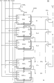
Fig. 4 is the block diagram according to the gate drivers of the liquid crystal display of example embodiment of the present invention that illustrates among Fig. 1.
With reference to Fig. 4, gate drivers 210 comprises that its cascade has the shift register 210a of a plurality of grades of SRC1-SRCn+1.Each level comprises the sub-IN1 of first input end, the first clock terminal CK1, second clock terminal CK2, the second input terminal IN2, the sub-Vin of voltage input end, replacement terminal RE, carry terminal CR and lead-out terminal OUT.
The sub-IN1 of the first input end of each grade among the level SRC2-SRCn+ 1 is electrically connected to the carry terminal CR of the last adjacent level among grade SRC1-SRCn to receive last carry signal.Yet the sub-IN1 of first input end of the first order SRC1 among the level SRC1-SRCn+ 1 receives the vertical commencing signal STV of the operation that starts gate drivers 210.The second input terminal IN2 of each grade among the level SRC1-SRCn is electrically connected to the lead-out terminal OUT of next adjacent level among grade SRC2-SRCn+ 1 to receive next signal.Yet the second input terminal IN2 of the rear class SRCn+1 of level among the SRC1-SRCn+ 1 receives vertical commencing signal STV.
Level SRC1, the SRC3 of the odd-numbered in the level SRC1-SRCn+ 1 ..., the first clock terminal CK1 of SRCn+1 applies the first clock signal CKV, and to level SRC1, the SRC3 of odd-numbered ..., the second clock terminal CK2 of SRCn+1 applies the second clock signal CKVB with phase place opposite with the first clock signal CKV.Equally, the level SRC2 of the even-numbered in the level SRC1-SRCn+ 1 ..., the first clock terminal CK1 of SRCn applies second clock signal CKVB, and to the level SRC2 of even-numbered ..., the second clock terminal CK2 of SRCn applies the first clock signal CKV.
The sub-Vin of voltage input end of each grade among the level SRC1-SRCn+ 1 receives ground voltage (not shown) or grid-cut-off voltage Voff.In addition, the carry terminal CR of rear class SRCn+1 is electrically connected to the replacement terminal RE of each grade among grade SRC1-SRCn+ 1.
The lead-out terminal OUT of level SRC1-SRCn+ 1 is electrically connected to respectively gate lines G L1-GLn.So level SRC1-SRCn+1 sequentially exports signal G1-Gn by lead-out terminal OUT, to apply signal G1-Gn to gate lines G L1-GLn.
Fig. 5 A be explanation in the general liquid crystal display the first grid signal and the signal of the relation between the data-signal and data-signal to the curve map of time, and Fig. 5 B is explanation according to the signal of the first grid signal in the liquid crystal display of example embodiment of the present invention and the relation between the data-signal and the data-signal curve map to the time.With reference to Fig. 5 A, because first utmost point in the general gate drivers does not have the adjacent formerly utmost point, so the first order receives vertical commencing signal STV with start-up operation with top with reference to the described mode of Fig. 4.
Further, the vertical commencing signal STV that is applied to general gate drivers has the high level lasting time longer than the duration of a horizontal scanning period.So, when applying vertical commencing signal to the first order, from first grid signal G ' 1 distortion between its decrement phase of first order output, as shown in Fig. 5 A.
When first grid signal G ' 1 distortion, before dropping to low level, first grid signal G ' 1 applies data-signal to data line.More specifically, in the display device that uses the line inversion driving method, the polarity of data-signal was inverted before first grid signal G ' 1 drops to low level.The result, when the data-signal with negative polarity that is applied to the first pixel column that is connected to first grid polar curve was reversed to before first grid signal G ' 1 drops to low level fully when having positive polarity, is charged to the negative polarity that the pixel voltage factor data signal of the first pixel column has and reduces.As a result, go out existing defective, cause the first pixel column to become brighter than other pixel column.
With reference to Fig. 5 B, earlier be discharged than signal G ' 1 according to the first grid signal G1 of example embodiment of the present invention.More specifically, produce t1 (with reference to Fig. 2) between the first high period of the first output enable signal OE1 owing to do sth. in advance about 1.8 microseconds, earlier export first grid signal G1 from gate drivers than signal G ' 1.Equally, produce t2 (with reference to Fig. 2) between the first high period of the second output enable signal OE2 owing to do sth. in advance about 1.8 microseconds, earlier first grid signal G1 is discharged than signal G ' 1.Thereby, can before applying data-signal D1~Dm to data line DL1~DLm, first grid signal G1 be discharged fully, thereby avoid on the display panels 100 distortion of the image that shows.
As a result, the first grid signal G1 of example embodiment of the present invention is in low level (Fig. 5 B) substantially when the polarity of data-signal is inverted.Thereby, avoid the first pixel column to be subjected to the adverse effect of the data-signal of next pixel column according to the gate drivers 210 of example embodiment of the present invention, thereby effectively prevent or reduce the line defect of the first pixel column of discussing according to prior art among top Fig. 5 A.
Fig. 6 A is the block diagram of the gate drivers of display device according to another exemplary embodiment of the present invention, and Fig. 6 B is the oscillogram according to the input and output signal of the illusory level D-SRC of the gate drivers of the display device of this example embodiment of the present invention among the key diagram 6A.Among Fig. 6 A, with identical or similar element among similar reference numerals designate Fig. 4, thereby the repeat specification that below will omit identical or analogous element.
With reference to Fig. 6 A, comprise shift register 220a and discharge circuit 220b according to the gate drivers 220 of example embodiment of the present invention.Shift register 220a comprises first to n+1 level SRC1-SRCn+ 1 and illusory level D-SRC.
With first to n level SRC1-SRCn be connected to display panel first to n gate lines G L1-GLn (Fig. 1), sequentially to export signal G1-Gn.N+1 level SRCn+ 1 is provided as close and after n level SRCn, is used for closing n level SRCn.More specifically, the dummy gate electrode signal that will export from the lead-out terminal OUT of n+1 level SRCn+ 1 is applied to the second input terminal IN2 of n level SRCn, being reduced to grid-cut-off voltage Voff from the signal GN of n level SRCn output.
Further, illusory level D-SRC be provided as near and before first order SRC 1, and operate in response to vertical commencing signal STV.To be applied to from the carry signal output D-CR of illusory level D-SRC output the sub-IN1 of first input end of first order SRC1.
With reference to Fig. 6 A and 6B, illusory level D-SRC between the high period of vertical commencing signal STV in response to second clock signal CKVB output carry signal D-CR.And first order SRC1 exports first grid signal G1 in response to the carry signal D-CR of illusory level D-SRC, so that gate drivers 220 avoids first grid signal G1 to be caused distortion by vertical commencing signal STV, describes in detail as top.
Because illusory level D-SRC drives first order SRC1, illusory level D-SRC is free of attachment to gate lines G L1-GLn.Thereby although caused distortion from the dummy gate electrode signal of the lead-out terminal OUT output of illusory level D-SRC by vertical commencing signal STV, the distortion of dummy gate electrode signal is not presented on the display panel.
As mentioned above, will output to first order SRC1 from the carry signal D-CR of illusory level D-SRC output and replace vertical commencing signal STV.Thereby, can avoid effectively preventing or reduce the line defect of the first pixel column of display panel from the distortion of the first grid signal of first order SRC1 output.
Fig. 7 is the block diagram that the gate drivers of display device according to another exemplary embodiment of the present invention is shown, Fig. 8 is the oscillogram according to the input and output signal of the pulse width modulator of the gate drivers of the display device of this example embodiment of the present invention in the key diagram 7, and Fig. 9 is the curve map according to the first grid signal output of the gate drivers of the display device of this example embodiment of the present invention in the key diagram 7.Among Fig. 7, with identical or similar element among similar reference numerals designate Fig. 4, thereby the repeat specification that below will omit identical or analogous element.
With reference to Fig. 7, gate drivers 230 according to another exemplary embodiment of the present invention comprises shift register 230a, pulse width modulator 230b and discharge circuit 230c.
With reference to Fig. 7 and 8, the first vertical commencing signal STV1 is maintained high state continue more than or equal to semiperiod of the first clock signal CKV and be less than or equal to time of the one-period T of the first clock signal CKV.Second clock signal CKVB has the phase place with the single spin-echo of the first clock signal CKV, so that between the high period of the first clock signal CKV second clock signal CKVB is maintained low level.So the transistor of pulse width modulator 230b is switched between the high period of second clock signal CKVB, and the output stage by pulse width modulator 230b is to first order SRC1 output the first vertical commencing signal STV1.
When second clock signal CKVB was converted to low level and the first clock signal CKV and is converted to high level, the transistor of pulse width modulator 230b was cut off and remain off between the low period of second clock signal CKVB.So, be applied to this transistorized first vertical commencing signal STV1 does not pass through pulse width modulator 230b between the low period of second clock signal CKVB transistor arrival first order SRC1.
As a result, the second vertical commencing signal STV2 has between half corresponding high period between high period with second clock signal CKVB and by the transistorized output stage from pulse width modulator 230b and outputs to first order SRC1.To be applied to from the second vertical commencing signal STV2 of pulse width modulator 230b output the sub-IN1 of first input end of the first order SRC1 of shift register 230a.
Among Fig. 9, the first grid signal G1 that 1 explanation of the first curve A is exported from first order SRC1 when applying the first vertical commencing signal STV1 to the sub-IN1 of the first input end of first order SRC1.The first grid signal G1 that 2 explanations of the second curve A are exported from first order SRC1 when applying the second vertical commencing signal STV2 to the sub-IN1 of the first input end of first order SRC1 according to the example embodiment of the invention described above.
With reference to Fig. 9, when applying the first vertical commencing signal STV1 to first order SRC1 (A1), from the negative edge distortion of the first grid signal G1 of first order SRC1 output.For example, when between the low period of the first clock signal CKV the first vertical commencing signal STV1 being maintained high level, first grid signal G1 reduces rapidly at the negative edge of the first clock signal CKV, causes distortion.
Should between the high period of second grid signal G2, first grid signal G1 be discharged into low level fully.Yet, because first grid signal G1 reduces rapidly at the negative edge of the first clock signal CKV as mentioned above, before changing high level into, second grid signal G2 has the interval, and for example produce first grid signal G1 be maintained at intermediate level between low level and the high level during, the first grid distorted signals.
Yet, in the example embodiment of the present invention of Fig. 7, when applying the vertical commencing signal STV2 of second shown in Fig. 8 to first order SRC1, the second vertical commencing signal STV2 changes low level into when the first clock signal CKV changes low level into, thereby avoids first grid signal G1 to reduce rapidly at the negative edge of the first clock signal CKV.So, first grid signal G1 maintained high level until produce second grid signal G2, and is low level by second grid signal G2 with first grid signal G1 discharge.Thereby, prevent distortion from the signal G1 output of first order SRC1 according to the gate drivers 230 of example embodiment of the present invention, shown in the A2 of Fig. 9.
Figure 10 is the schematic circuit of the first order SRC1 of gate drivers according to another exemplary embodiment of the present invention.A SRC1 who describes with reference to Figure 10 has the 26S Proteasome Structure and Function identical with other grade SRC2-SRCn+ 1 of gate drivers, thereby the repeat specification that below will omit other grade.
With reference to Figure 10, first order SRC1 comprise pull portion 211, carry portion 212, drop-down part 213, on draw drive part 214, anti-ripple (ripple preventing) part 215, retaining part 216, phase inverter part 217 and replacement part 218.
Drop-down part 213 comprises pull-down transistor NT3, and its control utmost point is connected to the second input terminal IN2, and the input utmost point is connected to the sub-Vin of voltage input end, and output stage is connected to lead-out terminal OUT.Pull-down transistor NT3 pulls down to the grid that provides by the sub-Vin of voltage input end-cut-off voltage Voff (Fig. 4) in response to next neighboring gates signal with signal.Select in the example embodiment of the present invention, for example can (but being not limited to) after horizontal scanning period receives, signal be pulled down to low level.
Drop-down drive part 214 comprises buffer transistor NT4, the first capacitor C1, the first discharge transistor NT5 and the second discharge transistor NT6, the 4th capacitor C4.Buffer transistor NT4 comprises the input utmost point that jointly is connected to the sub-IN1 of first input end and the output stage of controlling the utmost point and being connected to Q-node QN.The first capacitor C1 is connected between Q-node QN and the lead-out terminal OUT.The first discharge transistor NT5 comprises the input utmost point that is connected to Q-node QN, the control utmost point that is connected to the high sub-IN2 of the second input and the output stage that is connected to the sub-Vin of voltage input end.The second discharge transistor NT6 comprises the input utmost point that is connected to lead-out terminal OUT, is connected to the control utmost point of second clock terminal CK2 and the output stage that is connected to the sub-Vin of voltage input end.The 4th capacitor C4 is connected between Q-node QN and the carry terminal CR.
When buffer transistor NT4 in response to adjacent last signal during conducting, the first and the 4th capacitor C1 and C4 are recharged.When the voltage of the starting voltage that for example is higher than the NT1 that pulls up transistor was charged to the first capacitor C1, the electromotive force of Q-node QN was increased to and is higher than this starting voltage and the NT1 conducting that pulls up transistor.Equally, when the voltage of the starting voltage that for example is higher than carry transistor NT2 was charged to the 4th capacitor C4, the electromotive force of Q-node QN was increased to and is higher than this starting voltage and carry transistor NT2 conducting.So, export the first clock signal CKV to lead-out terminal OUT and carry terminal CR, so that signal and carry signal change high level into.Between a high period of the first clock signal CKV, signal is maintained high level.
When the first discharge transistor NT5 in response to next neighboring gates signal during conducting, the voltage that is charged to the first capacitor C1 is discharged by the first discharge transistor NT5 and is grid-cut-off voltage Voff.So the electromotive force of Q-node QN is reduced to grid-cut-off voltage Voff by adjacent next signal, the NT1 thereby cut-off pulls up transistor.Further, the first discharge transistor NT5 avoids signal to be output after relevant horizontal scanning period finishes.
When the second discharge transistor NT6 in response to the second clock signal CKVB that is applied to second clock terminal CK2 during conducting, lead-out terminal OUT is electrically connected to the sub-Vin of voltage input end by the second discharge transistor NT6.Thereby the signal of lead-out terminal OUT is grid-cut-off voltage Voff by the second discharge transistor NT6 discharge.
As described in detail later, anti-corrugated portion 215 prevents that signal from being caused ripple by the first clock signal CKV or second clock signal CKVB during last horizontal scanning period (n-1) H.Anti-corrugated portion 215 comprises the first anti-ripple transistor NT7 and the second anti-ripple transistor NT8.
The first anti-ripple transistor NT7 comprises the control utmost point that is connected to second clock terminal CK2, is connected to the input utmost point of the sub-IN1 of first input end and the output stage that is connected to Q-node QN.The second anti-ripple transistor NT8 comprises the control utmost point that is connected to the first clock terminal CK1, is connected to the input utmost point of Q-node QN and the output stage that is connected to lead-out terminal OUT.
First anti-ripple transistor NT7 conducting in response to the second clock signal CKVB that provides by second clock terminal CK2 is to be electrically connected the sub-IN1 of first input end and Q-node QN.Thereby the first anti-ripple transistor NT7 remains the last neighboring gates signal that maintains grid-cut-off voltage Voff with the electromotive force of Q-node QN.And then, the first anti-ripple transistor NT7 NT1 conducting between the high period of (n-1) H second clock signal CKVB in the cycle of avoiding pulling up transistor, thus prevent that signal from producing ripple.
The second anti-ripple transistor NT8 is in response to the conducting by the first clock signal CKV, lead-out terminal OUT is electrically connected to Q-node QN.So, the electromotive force of Q-node QN is remained the signal that maintains grid-cut-off voltage Voff.As a result, the second anti-ripple transistor NT8 NT1 conducting between the high period of (n-1) H first clock signal CKV in the cycle of avoiding pulling up transistor, thus prevent that signal from producing ripple.
Retaining part 216 comprises maintenance transistor NT10, and its control utmost point is connected to the output of phase inverter part 217, and the input utmost point is connected to the sub-Vin of voltage input end, and output stage is connected to lead-out terminal OUT.
The first inverter transistor NT11 comprises the input utmost point that jointly is connected to the first clock terminal CK1 and the output stage of controlling the utmost point and being connected to the output stage of the second inverter transistor NT12 by the 3rd capacitor C3.The second inverter transistor NT12 comprises the input utmost point that is connected to the first clock terminal CK1, is connected to the control utmost point of its input utmost point and the output stage that is connected to the control utmost point that keeps transistor NT10 by the second capacitor C2.The 3rd inverter transistor NT13 comprise the output stage that is connected to the first inverter transistor NT11 the input utmost point, be connected to the control utmost point of lead-out terminal OUT and the output stage that is connected to the sub-Vin of voltage input end.The 4th inverter transistor NT14 comprises the input utmost point that is connected to the control utmost point that keeps transistor NT10, is connected to the control utmost point of lead-out terminal OUT and the output stage that is connected to the sub-Vin of voltage input end.
The third and fourth inverter transistor NT13 and NT14 be the conducting in response to the signal that is in high level of the lead-out terminal OUT by being in high level respectively, and is discharged from the first clock signal CKV of the first and second inverter transistor NT11 and NT12 output respectively and is grid-cut-off voltage Voff.So, keep transistor NT10 when current signal is maintained at high level, being cut off during the horizontal scanning period 1H.When current signal changed low level into, the third and fourth inverter transistor NT13 and NT14 were cut off.So, keep transistor NT10 in response to inputting CKV and conducting from the first clock of the first and second inverter transistor NT11 and NT12 output respectively.As a result, between the high period of the first clock signal CKV during last horizontal scanning period (n-1) H, by maintenance transistor NT10 current signal is remained on grid-cut-off voltage.
In the example embodiment of the present invention, the pull-down transistor NT3 of first order SRC1 has the channel width more than or equal to about twice of the channel width of the pull-down transistor NT3 of level SRC2-SRCn.More specifically, the of the present invention selection in the example embodiment, the pull-down transistor NT3 of first order SRC1 can have about 3000 microns channel width, and the pull-down transistor NT3 of each grade among the level SRC2-SRCn can have about 1100 microns channel width, but is not limited to this.
Pull-down transistor NT3 is grid-cut-off voltage Voff in response to adjacent next signal with the signal discharge.When the channel width of the pull-down transistor NT3 of first order SRC1 during greater than the channel width of the pull-down transistor NT3 of level SRC2-SRCn, the discharge capability of first order SRC1 is enhanced.So, describe in detail with reference to Fig. 5 B as top, even if Q-node QN does not have to be discharged rapidly in first order SRC1 because of vertical commencing signal STV, the first grid signal G1 of output also can be discharged rapidly from first order SRC1 to gate lines G L1, and first grid signal G1 is corresponding to fast reducing with the negative edge of the first clock signal CKV.
Thereby, because the ability of the pull-down transistor NT3 of first order SRC1 is improved because of the channel width of the pull-down transistor NT3 of the first order SRC1 channel width greater than the pull-down transistor NT3 of level SRC2-SRCn, first grid signal G1 is discharged rapidly, thereby avoids the distortion of first grid signal G1.
Being connected to first grid polar curve GL1 is used for the discharge transistor NT16 of first grid signal G1 discharge is had more than or equal to being connected to 1.5 times the channel width of gate lines G L2-GLn for the channel width of the discharge transistor NT16 that signal G2-Gn is discharged.More specifically, the discharge transistor NT16 that is connected to first grid polar curve GL1 can have about 6000 microns channel width, and the discharge transistor NT16 that is connected to gate lines G L2-GLn can have about 4000 microns channel width.
So, the discharge capability of the discharge transistor NT16 of first grid signal G1 discharge compared with the discharge capability of the discharge transistor NT16 that is connected to gate lines G L2-GLn be improved, thereby first grid signal G1 is discharged rapidly, avoid the distortion of first grid signal G1.
The the first anti-ripple transistor NT7 that is connected to the Q-node QN of first order SRC1 can have about 1/10th channel width of the channel width of the first anti-ripple transistor NT7 that is less than or equal to grade SRC2-SRCn.More specifically, the first anti-ripple transistor NT7 of first order SRC1 can have about 25 microns channel width, and the first anti-ripple transistor NT7 of level SRC2-SRCn can have about 350 microns channel width.
The anti-ripple transistor NT7 of among the first order SRC1 first applies vertical commencing signal STV in response to second clock signal CKVB to Q-node QN.Yet, if the ability of the anti-ripple transistor NT7 of first among the first order SRC1 is degenerated, for example the channel width of first of first order SRC1 the anti-ripple transistor NT7 has increased, and then the increase of the electromotive force of Q-node QN may be delayed because vertical commencing signal STV has high level between the high period of second clock signal CKVB.Thereby, as mentioned above, compare with the relevant transistor channel width separately among the level SRC2-SRCn, the channel width of pull-down transistor NT3 and discharge transistor NT16 is relatively large among the first order SRC1, and the channel width of the first anti-ripple transistor NT7 is less, in order to effectively reduce or avoid the distortion of first grid signal G1.
In the example embodiment of the present invention, first order SRC1 is placed outer peripheral areas near display panel so that with other grade SRC2-SRCn in compare the transistorized channel width that can easily strengthen first order SRC1.
Figure 11 A is the planimetric map according to the first anti-ripple transistor NT7 of the first order SRC1 of the gate drivers of this example embodiment of the present invention among Figure 10, and Figure 11 B is the planimetric map according to the first anti-ripple transistor NT7 of the second level SRC2 of the gate drivers of this example embodiment of the present invention among Figure 10.
With reference to Figure 11 A and 11B, the first anti-ripple transistor NT7 of first order SRC1 comprises first grid GE1, the first source S E1 and the first drain D E1.The first anti-ripple transistor NT7 of second level SRC2 comprises second grid GE2, the second source S E2 and the second drain D E2.As shown in Figure 11 A and 11B, the first anti-ripple transistor NT7 of first order SRC1 has the narrower channel width W1 of channel width W2 than the first anti-ripple transistor NT7 of second level SRC2.
In the example embodiment of the present invention, the first anti-ripple transistor NT7 of first order SRC1 has about 25 microns channel width, and the first anti-ripple transistor NT7 of second level SRC2 has about 350 microns channel width.
As mentioned above, when first of first order SRC1 prevents that the channel width W1 of ripple transistor NT7 prevents the channel width W2 of ripple transistor NT7 less than first of second level SRC2, can effectively reduce or avoid the clock of first grid signal G1.Yet when first of first order SRC1 prevented that the channel width of ripple transistor NT7 reduces, the ripple voltage at the Q-node QN place of first order SRC1 may increase.More specifically, the ripple voltage at the Q-node QN place of first order SRC1 is inversely proportional with the total capacitance of the capacitor that is connected to Q-node QN.For example, when the total capacitance that comprises stray capacitance that is connected to Q-node QN increased, the ripple voltage at Q-node QN place reduced.
Thereby, the first anti-ripple transistor NT7 of first order SRC1 is designed to have the stray capacitance that equates with the stray capacitance of the first anti-ripple transistor NT7 of second level SRC2.
More specifically, first of first order SRC1 the anti-ripple transistor NT7 is included in the first capacitor parasitics Cgs1 that forms between first grid GE1 and the first source S E1 and the second capacitor parasitics Cgd1 that forms between first grid GE1 and the first drain D E1.The first anti-ripple transistor NT7 of second level SRC2 is included in the trixenie capacitor Cgs2 that forms between second grid GE2 and the second source S E2 and the 4th capacitor parasitics Cgd2 that forms between second grid GE2 and the second drain D E2, so that the first anti-ripple transistor NT7 stray capacitance of first order SRC1 equates substantially with the stray capacitance of the first anti-ripple transistor NT7 of second level SRC2.
More specifically, in example embodiment of the present invention, the size of the first source S E1 is such, so that the overlapping region between the first source S E1 and the first grid GE1 equals the overlapping region between the second source S E2 and the second grid GE2.So the first capacitor parasitics Cgs1 has the electric capacity that equates with trixenie capacitor Cgs2.
In addition, the size of the first drain D E1 is such, so that the overlapping region between the first drain D E1 and the first grid GE1 equals the overlapping region between the second drain D E2 and the second grid GE2.So the second capacitor parasitics Cgd1 has the electric capacity that equates with the 4th capacitor parasitics Cgd2.
Thereby the total capacitance of capacitor that is connected to the Q-node QN of first order SRC1 does not reduce, in order to effectively reduce or avoid the ripple voltage at Q-node QN place.
According to example embodiment of the present invention described herein, the moment that can be inverted than the polarity of data-signal wherein will be reduced to low level from the first grid signal of the first order output of gate drivers quickly.So, can effectively reduce or substantially avoid the line defect of the first pixel column, thereby improve the display quality of display device.
In addition, owing to for example use the first order that replaces commencing signal control gate driver such as the signal from the carry signal of illusory level, undistorted from the first grid signal of first order output in the example embodiment of the present invention described herein.Thereby, can further effectively reduce or substantially avoid the line defect of the first pixel column, thereby further improve the display quality of display device.
The present invention should not be read as and be limited to its example embodiment described herein.On the contrary, it is in order to make the disclosure thoroughly and complete that these example embodiment are provided, and passes on all sidedly concept of the present invention to those skilled in the art.
Although showed particularly with reference to its example embodiment and described the present invention, but it should be understood by one skilled in the art that those of ordinary skills can make therein various changes and modification and do not deviate from the spirit and scope of the present invention that limited by appended claims.
Cross reference to related application
The application requires the right of priority of the korean patent application No.2007-23216 of submission on March 8th, 2007, and its full content is incorporated in this by reference.
Claims (9)
1. display device comprises:
Timing controller, its output image data, the first output enable signal, the second output enable signal, clock generating signal, vertical commencing signal and data controlling signal, wherein, described the second output enable signal has the phase place different from described the first output enable signal;
Clock generator, it produces the first clock signal and second clock signal according to described the first output enable signal, described the second output enable signal and described clock generating signal, wherein, the first clock of described the first clock signal is earlier changed in high state by described the first output enable signal, and is earlier changed in low state by described the second output enable signal;
Gate drivers, it sequentially exports signal in response to described the first clock signal, described second clock signal and described vertical commencing signal, wherein, the first grid signal of described signal is corresponding to described first clock of described the first clock signal;
Data driver, it is converted to data-signal in response to described data controlling signal with described view data; And
Display panel comprises:
Many gate lines, it sequentially receives described signal;
Many data lines, it receives described data-signal; And
Be connected to a plurality of pixels of described many grids and described many data lines, it receives described data-signal with the demonstration image in response to described signal,
Wherein said first grid signal was discharged before described data-signal is applied to described data line fully,
Wherein, described the first clock signal rises to high level in response to the rising edge of described the first output enable signal, and drops to low level in response to the rising edge of described the second output enable signal, and
Wherein, described second clock signal response is in the rising edge of described the second output enable signal and rise to high level, and drops to low level in response to the rising edge of described the first output enable signal.
2. display device as claimed in claim 1, wherein said vertical commencing signal is used for starting the operation of described gate drivers;
Described the first clock signal is used for determining being applied to duration of signal of gate line of the odd-numbered of described many gate lines; And
Described second clock signal is used for determining being applied to duration of signal of gate line of the even-numbered of described many gate lines, and has the phase place with the single spin-echo of described the first clock signal.
3. display device as claimed in claim 2, equal described the first output enable signal transition during wherein said the first clock signal and be the first output enable signal the first high state first constantly and described the second output enable signal transition be second duration between constantly of the second output enable signal the first high state.
4. display device as claimed in claim 3, in wherein said the first output enable signal, described the second output enable signal and the described clock generating signal each has identical frequency, equals the overlapping period between described clock generating signal and described the second output enable signal between the decrement phase of described the first clock signal.
5. display device as claimed in claim 3, the duration of the duration of wherein said the first output enable signal the first high state and described the second output enable signal the first high state is separately respectively more than or equal to the duration of the follow-up high state of the first output enable signal and the duration of the follow-up high state of the second output enable signal.
6. method that drives display device, the method comprises:
Output image data, the first output enable signal, the second output enable signal, clock generating signal, vertical commencing signal and data controlling signal, wherein, described the second output enable signal has the phase place different from described the first output enable signal;
Produce the first clock signal and second clock signal according to described the first output enable signal, described the second output enable signal and described clock generating signal, wherein, the first clock of described the first clock signal is earlier changed in high state by described the first output enable signal, and is earlier changed in low state by described the second output enable signal;
Sequentially export signal in response to described the first clock signal, described second clock signal and described vertical commencing signal, wherein, the first grid signal of described signal is corresponding to described first clock of described the first clock signal;
In response to described data controlling signal described view data is converted to data-signal;
Exported described data-signal after the discharge fully at described first grid signal; And
Receive described data-signal with the demonstration image in response to described signal,
Wherein, described the first clock signal rises to high level in response to the rising edge of described the first output enable signal, and drops to low level in response to the rising edge of described the second output enable signal, and
Wherein, described second clock signal response is in the rising edge of described the second output enable signal and rise to high level, and drops to low level in response to the rising edge of described the first output enable signal.
7. method as claimed in claim 6, wherein:
Described vertical commencing signal is used for starting the output of described first grid signal;
Between the high period of described the first clock signal for the signal of the odd-numbered of determining described signal; And
Described second clock signal be used for to determine between the high period of signal of even-numbered of described signal, and has the phase place with the single spin-echo of described the first clock signal.
8. method as claimed in claim 6, equal described the first output enable signal transition during wherein said the first clock signal and be the first output enable signal the first high state first constantly and described the second output enable signal transition be second duration between constantly of the second output enable signal the first high state.
9. method as claimed in claim 8, the duration of wherein said the first output enable signal the first high state and described the second output enable signal the first high state is respectively more than or equal to the duration of the follow-up high state of the first output enable signal and the duration of the follow-up high state of the second output enable signal.
Applications Claiming Priority (2)
| Application Number | Priority Date | Filing Date | Title |
|---|---|---|---|
| KR1020070023126A KR101375863B1 (en) | 2007-03-08 | 2007-03-08 | Display apparatus and method of driving the same |
| KR23126/07 | 2007-03-08 |
Related Child Applications (1)
| Application Number | Title | Priority Date | Filing Date |
|---|---|---|---|
| CN201110087342.8A Division CN102141711B (en) | 2007-03-08 | 2008-03-07 | Display apparatus and method of driving the same |
Publications (2)
| Publication Number | Publication Date |
|---|---|
| CN101261412A CN101261412A (en) | 2008-09-10 |
| CN101261412B true CN101261412B (en) | 2013-05-01 |
Family
ID=39741170
Family Applications (2)
| Application Number | Title | Priority Date | Filing Date |
|---|---|---|---|
| CN201110087342.8A Active CN102141711B (en) | 2007-03-08 | 2008-03-07 | Display apparatus and method of driving the same |
| CN2008100831283A Active CN101261412B (en) | 2007-03-08 | 2008-03-07 | Display apparatus and method of driving the same |
Family Applications Before (1)
| Application Number | Title | Priority Date | Filing Date |
|---|---|---|---|
| CN201110087342.8A Active CN102141711B (en) | 2007-03-08 | 2008-03-07 | Display apparatus and method of driving the same |
Country Status (4)
| Country | Link |
|---|---|
| US (2) | US8305323B2 (en) |
| JP (1) | JP5430870B2 (en) |
| KR (1) | KR101375863B1 (en) |
| CN (2) | CN102141711B (en) |
Families Citing this family (50)
| Publication number | Priority date | Publication date | Assignee | Title |
|---|---|---|---|---|
| US20110001732A1 (en) * | 2008-02-19 | 2011-01-06 | Hideki Morii | Shift register circuit, display device, and method for driving shift register circuit |
| US20110234565A1 (en) * | 2008-12-12 | 2011-09-29 | Sharp Kabushiki Kaisha | Shift register circuit, display device, and method for driving shift register circuit |
| KR101542509B1 (en) * | 2008-12-24 | 2015-08-06 | 삼성디스플레이 주식회사 | Gate driving device and liquid crystal display comprising therein |
| TWI406222B (en) * | 2009-05-26 | 2013-08-21 | Chunghwa Picture Tubes Ltd | Gate driver having an output enable control circuit |
| WO2010150607A1 (en) * | 2009-06-25 | 2010-12-29 | Semiconductor Energy Laboratory Co., Ltd. | Display device and electronic device |
| CN102024431B (en) * | 2009-09-16 | 2013-04-03 | 北京京东方光电科技有限公司 | TFT-LCD driving circuit |
| KR101101105B1 (en) * | 2009-11-04 | 2012-01-03 | 삼성모바일디스플레이주식회사 | Emission Driver and Organic Light Emitting Display Device Using the same |
| KR101605435B1 (en) * | 2009-12-14 | 2016-03-23 | 삼성디스플레이 주식회사 | Display panel |
| KR101752834B1 (en) * | 2009-12-29 | 2017-07-03 | 삼성디스플레이 주식회사 | Gate driving circuit and display apparatus having the same |
| US8957843B2 (en) * | 2010-02-25 | 2015-02-17 | Samsung Display Co., Ltd. | Gate selection circuit of liquid crystal panel, accumulating capacity driving circuit, driving device, and driving method |
| KR101710661B1 (en) * | 2010-04-29 | 2017-02-28 | 삼성디스플레이 주식회사 | Gate driving circuit and display apparatus having the same |
| TWI433093B (en) * | 2010-12-16 | 2014-04-01 | Chunghwa Picture Tubes Ltd | Method for reducing double images |
| CN202008813U (en) | 2010-12-23 | 2011-10-12 | 北京京东方光电科技有限公司 | Grid driver of TFT LCD, drive circuit, and LCD |
| JP2012150215A (en) * | 2011-01-18 | 2012-08-09 | Japan Display East Co Ltd | Display device |
| KR101778650B1 (en) * | 2011-02-23 | 2017-09-15 | 삼성디스플레이 주식회사 | Display panel and display apparatus having the same |
| KR101481675B1 (en) * | 2011-10-04 | 2015-01-22 | 엘지디스플레이 주식회사 | Bidirectional shift register |
| TWI493871B (en) * | 2012-06-05 | 2015-07-21 | Au Optronics Corp | Shift register circuitry, display and shift register |
| KR102015396B1 (en) | 2012-11-27 | 2019-08-28 | 엘지디스플레이 주식회사 | Shift register and method for driving the same |
| CN104700808B (en) * | 2013-06-06 | 2017-08-25 | 青岛海信电器股份有限公司 | Display device, time schedule controller and method for displaying image |
| CN104700810A (en) * | 2013-06-06 | 2015-06-10 | 青岛海信电器股份有限公司 | Display device, time sequence controller and image display method |
| TWI512701B (en) * | 2013-08-08 | 2015-12-11 | Novatek Microelectronics Corp | Liquid crystal display and gate driver thereof |
| KR102114155B1 (en) * | 2013-10-01 | 2020-05-25 | 삼성디스플레이 주식회사 | Display device and driving method thereof |
| KR102031365B1 (en) * | 2013-11-08 | 2019-10-11 | 엘지디스플레이 주식회사 | Scan Driver and Display Device Using the same |
| CN103700334B (en) * | 2013-12-19 | 2014-12-17 | 京东方科技集团股份有限公司 | Ramp signal generation circuit, signal generator, array substrate and display device |
| CN106132295B (en) | 2014-04-04 | 2019-12-13 | 奥托立夫开发公司 | driver and passenger information detection device |
| CN104299554B (en) * | 2014-08-22 | 2017-07-18 | 京东方科技集团股份有限公司 | Shift register, array base palte and display device |
| KR102250309B1 (en) * | 2014-10-13 | 2021-05-12 | 삼성디스플레이 주식회사 | Display device and Driving method of display device |
| FR3030902B1 (en) | 2014-12-17 | 2018-04-13 | Continental Automotive France | PORTABLE DEVICE FOR RADIOFREQUENCY WITH ADJUSTABLE GAIN AND ASSOCIATED GAIN ADJUSTMENT METHOD |
| CN104464596A (en) * | 2014-12-22 | 2015-03-25 | 合肥鑫晟光电科技有限公司 | Grid integrated drive circuit, display panel and display device |
| KR20160082401A (en) * | 2014-12-26 | 2016-07-08 | 삼성디스플레이 주식회사 | Method of driving display panel and display apparatus for performing the same |
| KR102282028B1 (en) * | 2015-01-14 | 2021-07-29 | 삼성디스플레이 주식회사 | Gate driving circuit |
| CN104658466B (en) * | 2015-01-27 | 2017-05-10 | 京东方科技集团股份有限公司 | GOA circuit and driving method thereof, as well as display panel and display device |
| CN104637431B (en) * | 2015-02-05 | 2019-03-15 | 京东方科技集团股份有限公司 | The method of GOA circuit and driving method, flexible display device and control display |
| CN106328026A (en) * | 2015-06-17 | 2017-01-11 | 南京瀚宇彩欣科技有限责任公司 | Liquid crystal display and dot inversion balance driving method thereof |
| US10037738B2 (en) * | 2015-07-02 | 2018-07-31 | Apple Inc. | Display gate driver circuits with dual pulldown transistors |
| US10809855B2 (en) * | 2015-08-19 | 2020-10-20 | Novatek Microelectronics Corp. | Driving circuit and a method for driving a display panel having a touch panel |
| KR102549431B1 (en) * | 2015-11-27 | 2023-06-30 | 삼성디스플레이 주식회사 | Display apparatus |
| KR102481068B1 (en) * | 2016-01-04 | 2022-12-27 | 삼성디스플레이 주식회사 | Display device |
| KR102536161B1 (en) * | 2016-03-31 | 2023-05-25 | 삼성디스플레이 주식회사 | Scan driver and display apparatus having the same |
| KR102578838B1 (en) * | 2016-09-30 | 2023-09-18 | 엘지디스플레이 주식회사 | Gate Driving Unit and Display Device Having the same |
| KR102556084B1 (en) | 2016-10-07 | 2023-07-17 | 삼성디스플레이 주식회사 | Display device capable of changing frame rate and operating method thereof |
| KR102503690B1 (en) * | 2016-12-30 | 2023-02-24 | 엘지디스플레이 주식회사 | Thin film transistor array substrate and display device including the same |
| CN106847221A (en) * | 2017-03-20 | 2017-06-13 | 京东方科技集团股份有限公司 | Shift register cell, gate driving circuit and driving method |
| JP7092279B2 (en) * | 2017-08-16 | 2022-06-28 | 京東方科技集團股▲ふん▼有限公司 | Array board row drive circuit |
| US10475408B2 (en) * | 2017-11-07 | 2019-11-12 | Shenzhen China Star Optoelectronics Semiconductor Display Technology Co., Ltd | Liquid crystal display panel with a polarity reversion and gate driving circuit thereof |
| CN107767832B (en) * | 2017-11-07 | 2020-02-07 | 深圳市华星光电半导体显示技术有限公司 | Liquid crystal display panel and grid drive circuit |
| CN109686334B (en) * | 2019-02-18 | 2021-01-22 | 京东方科技集团股份有限公司 | Gate drive circuit, drive method thereof and display device |
| WO2020243883A1 (en) * | 2019-06-03 | 2020-12-10 | 京东方科技集团股份有限公司 | Pixel circuit, pixel circuit driving method, and display apparatus and driving method therefor |
| KR20210086319A (en) * | 2019-12-31 | 2021-07-08 | 엘지디스플레이 주식회사 | Display device and driving method thereof |
| CN111883082B (en) * | 2020-07-30 | 2021-11-09 | 惠科股份有限公司 | Grid driving circuit, driving method and display |
Citations (2)
| Publication number | Priority date | Publication date | Assignee | Title |
|---|---|---|---|---|
| CN1530903A (en) * | 2003-03-17 | 2004-09-22 | 株式会社日立制作所 | Displaying device and driving method thereof |
| CN1809862A (en) * | 2002-08-30 | 2006-07-26 | 三星电子株式会社 | Liquid crystal display apparatus |
Family Cites Families (11)
| Publication number | Priority date | Publication date | Assignee | Title |
|---|---|---|---|---|
| US6275086B1 (en) * | 1998-11-19 | 2001-08-14 | Fujitsu Limited | Clock signal generator for an integrated circuit |
| CN100428319C (en) * | 2002-04-08 | 2008-10-22 | 三星电子株式会社 | Liquid crystal display device |
| WO2003104879A2 (en) * | 2002-06-01 | 2003-12-18 | Samsung Electronics Co., Ltd. | Shift register, liquid crystal display device having the shift register and method of driving scan lines using the same |
| KR100496542B1 (en) * | 2002-08-29 | 2005-06-22 | 엘지.필립스 엘시디 주식회사 | Liquid crystal display apparatus of 2-dot inversion type and method of dirving the same |
| KR101003586B1 (en) | 2003-12-26 | 2010-12-22 | 엘지디스플레이 주식회사 | Driving method of liquid crystal display |
| KR101030528B1 (en) | 2004-05-27 | 2011-04-26 | 엘지디스플레이 주식회사 | The shift resistor and the liquid crystal display device using the same |
| KR101031667B1 (en) * | 2004-12-29 | 2011-04-29 | 엘지디스플레이 주식회사 | Liquid crystal display device |
| KR101109841B1 (en) | 2004-12-31 | 2012-02-13 | 엘지디스플레이 주식회사 | Liquid crystal display device and unit for driving the same |
| KR101146531B1 (en) * | 2005-04-26 | 2012-05-25 | 삼성전자주식회사 | Display device and a driving apparatus thereof and method driving thereof |
| KR101117991B1 (en) * | 2005-06-08 | 2012-03-06 | 엘지디스플레이 주식회사 | Apparatus for driving liquid crystal display device |
| KR101158899B1 (en) | 2005-08-22 | 2012-06-25 | 삼성전자주식회사 | Liquid crystal display device, and method for driving thereof |
-
2007
- 2007-03-08 KR KR1020070023126A patent/KR101375863B1/en active IP Right Grant
- 2007-12-19 US US11/960,131 patent/US8305323B2/en active Active
-
2008
- 2008-03-07 CN CN201110087342.8A patent/CN102141711B/en active Active
- 2008-03-07 CN CN2008100831283A patent/CN101261412B/en active Active
- 2008-03-10 JP JP2008059459A patent/JP5430870B2/en active Active
-
2012
- 2012-10-04 US US13/644,685 patent/US8537095B2/en active Active
Patent Citations (2)
| Publication number | Priority date | Publication date | Assignee | Title |
|---|---|---|---|---|
| CN1809862A (en) * | 2002-08-30 | 2006-07-26 | 三星电子株式会社 | Liquid crystal display apparatus |
| CN1530903A (en) * | 2003-03-17 | 2004-09-22 | 株式会社日立制作所 | Displaying device and driving method thereof |
Also Published As
| Publication number | Publication date |
|---|---|
| KR101375863B1 (en) | 2014-03-17 |
| JP5430870B2 (en) | 2014-03-05 |
| KR20080082356A (en) | 2008-09-11 |
| US20080218502A1 (en) | 2008-09-11 |
| CN102141711B (en) | 2014-08-20 |
| US8305323B2 (en) | 2012-11-06 |
| US8537095B2 (en) | 2013-09-17 |
| JP2008225476A (en) | 2008-09-25 |
| US20130027287A1 (en) | 2013-01-31 |
| CN101261412A (en) | 2008-09-10 |
| CN102141711A (en) | 2011-08-03 |
Similar Documents
| Publication | Publication Date | Title |
|---|---|---|
| CN101261412B (en) | Display apparatus and method of driving the same | |
| CN101122720B (en) | Gate driver and display apparatus having the same | |
| JP4648699B2 (en) | Shift register, gate drive circuit and display panel using the same | |
| US8400390B2 (en) | Gate driving device and liquid crystal display having the same | |
| KR101167663B1 (en) | Gate Pole Driving Circuit and Liquid Crystal Display Having the Same | |
| US7283603B1 (en) | Shift register with four phase clocks | |
| KR101547565B1 (en) | Display and driving method of the same | |
| KR101281498B1 (en) | Gate driving circuit and display apparatus having the same | |
| CN101149500B (en) | Liquid crystal display apparatus | |
| CN107749281B (en) | Grid driving circuit | |
| CN101499252B (en) | Gate driving circuit | |
| KR20090081850A (en) | Gate deiver circuit and display apparatus having the same | |
| CN102622984B (en) | Display device and driving method thereof | |
| KR20100083370A (en) | Gate driving circuit and display device having the same | |
| US8786542B2 (en) | Display device including first and second scanning signal line groups | |
| KR102309625B1 (en) | Gate driving circuit, driving metohd for gate driving circuit and display panel using the same | |
| US9129575B2 (en) | Liquid crystal display device | |
| KR101394925B1 (en) | Liquid crystal display device and driving method thereof | |
| KR20080041894A (en) | Liquid crystal display | |
| KR20060096674A (en) | Test method for thin film transistor substrate | |
| KR20070076065A (en) | Liquid crystal display |
Legal Events
| Date | Code | Title | Description |
|---|---|---|---|
| C06 | Publication | ||
| PB01 | Publication | ||
| C10 | Entry into substantive examination | ||
| SE01 | Entry into force of request for substantive examination | ||
| ASS | Succession or assignment of patent right |
Owner name: SAMSUNG MONITOR CO., LTD. Free format text: FORMER OWNER: SAMSUNG ELECTRONICS CO., LTD. Effective date: 20121031 |
|
| C41 | Transfer of patent application or patent right or utility model | ||
| TA01 | Transfer of patent application right |
Effective date of registration: 20121031 Address after: Gyeonggi Do, South Korea Applicant after: Samsung Display Co., Ltd. Address before: Gyeonggi Do, South Korea Applicant before: Samsung Electronics Co., Ltd. |
|
| C14 | Grant of patent or utility model | ||
| GR01 | Patent grant |