CN101123289A - Bidirectional luminescent heat radiation LED - Google Patents
Bidirectional luminescent heat radiation LED Download PDFInfo
- Publication number
- CN101123289A CN101123289A CNA2007100300608A CN200710030060A CN101123289A CN 101123289 A CN101123289 A CN 101123289A CN A2007100300608 A CNA2007100300608 A CN A2007100300608A CN 200710030060 A CN200710030060 A CN 200710030060A CN 101123289 A CN101123289 A CN 101123289A
- Authority
- CN
- China
- Prior art keywords
- light
- led
- lens cap
- heat radiation
- wafer
- Prior art date
- Legal status (The legal status is an assumption and is not a legal conclusion. Google has not performed a legal analysis and makes no representation as to the accuracy of the status listed.)
- Pending
Links
Images


Classifications
-
- H—ELECTRICITY
- H01—ELECTRIC ELEMENTS
- H01L—SEMICONDUCTOR DEVICES NOT COVERED BY CLASS H10
- H01L2224/00—Indexing scheme for arrangements for connecting or disconnecting semiconductor or solid-state bodies and methods related thereto as covered by H01L24/00
- H01L2224/01—Means for bonding being attached to, or being formed on, the surface to be connected, e.g. chip-to-package, die-attach, "first-level" interconnects; Manufacturing methods related thereto
- H01L2224/42—Wire connectors; Manufacturing methods related thereto
- H01L2224/47—Structure, shape, material or disposition of the wire connectors after the connecting process
- H01L2224/48—Structure, shape, material or disposition of the wire connectors after the connecting process of an individual wire connector
- H01L2224/4805—Shape
- H01L2224/4809—Loop shape
- H01L2224/48091—Arched
-
- H—ELECTRICITY
- H01—ELECTRIC ELEMENTS
- H01L—SEMICONDUCTOR DEVICES NOT COVERED BY CLASS H10
- H01L2224/00—Indexing scheme for arrangements for connecting or disconnecting semiconductor or solid-state bodies and methods related thereto as covered by H01L24/00
- H01L2224/01—Means for bonding being attached to, or being formed on, the surface to be connected, e.g. chip-to-package, die-attach, "first-level" interconnects; Manufacturing methods related thereto
- H01L2224/42—Wire connectors; Manufacturing methods related thereto
- H01L2224/47—Structure, shape, material or disposition of the wire connectors after the connecting process
- H01L2224/48—Structure, shape, material or disposition of the wire connectors after the connecting process of an individual wire connector
- H01L2224/481—Disposition
- H01L2224/48151—Connecting between a semiconductor or solid-state body and an item not being a semiconductor or solid-state body, e.g. chip-to-substrate, chip-to-passive
- H01L2224/48221—Connecting between a semiconductor or solid-state body and an item not being a semiconductor or solid-state body, e.g. chip-to-substrate, chip-to-passive the body and the item being stacked
- H01L2224/48245—Connecting between a semiconductor or solid-state body and an item not being a semiconductor or solid-state body, e.g. chip-to-substrate, chip-to-passive the body and the item being stacked the item being metallic
- H01L2224/48247—Connecting between a semiconductor or solid-state body and an item not being a semiconductor or solid-state body, e.g. chip-to-substrate, chip-to-passive the body and the item being stacked the item being metallic connecting the wire to a bond pad of the item
-
- H—ELECTRICITY
- H01—ELECTRIC ELEMENTS
- H01L—SEMICONDUCTOR DEVICES NOT COVERED BY CLASS H10
- H01L2224/00—Indexing scheme for arrangements for connecting or disconnecting semiconductor or solid-state bodies and methods related thereto as covered by H01L24/00
- H01L2224/01—Means for bonding being attached to, or being formed on, the surface to be connected, e.g. chip-to-package, die-attach, "first-level" interconnects; Manufacturing methods related thereto
- H01L2224/42—Wire connectors; Manufacturing methods related thereto
- H01L2224/47—Structure, shape, material or disposition of the wire connectors after the connecting process
- H01L2224/48—Structure, shape, material or disposition of the wire connectors after the connecting process of an individual wire connector
- H01L2224/481—Disposition
- H01L2224/48151—Connecting between a semiconductor or solid-state body and an item not being a semiconductor or solid-state body, e.g. chip-to-substrate, chip-to-passive
- H01L2224/48221—Connecting between a semiconductor or solid-state body and an item not being a semiconductor or solid-state body, e.g. chip-to-substrate, chip-to-passive the body and the item being stacked
- H01L2224/48245—Connecting between a semiconductor or solid-state body and an item not being a semiconductor or solid-state body, e.g. chip-to-substrate, chip-to-passive the body and the item being stacked the item being metallic
- H01L2224/48257—Connecting between a semiconductor or solid-state body and an item not being a semiconductor or solid-state body, e.g. chip-to-substrate, chip-to-passive the body and the item being stacked the item being metallic connecting the wire to a die pad of the item
-
- H—ELECTRICITY
- H01—ELECTRIC ELEMENTS
- H01L—SEMICONDUCTOR DEVICES NOT COVERED BY CLASS H10
- H01L2224/00—Indexing scheme for arrangements for connecting or disconnecting semiconductor or solid-state bodies and methods related thereto as covered by H01L24/00
- H01L2224/80—Methods for connecting semiconductor or other solid state bodies using means for bonding being attached to, or being formed on, the surface to be connected
- H01L2224/85—Methods for connecting semiconductor or other solid state bodies using means for bonding being attached to, or being formed on, the surface to be connected using a wire connector
- H01L2224/85909—Post-treatment of the connector or wire bonding area
- H01L2224/8592—Applying permanent coating, e.g. protective coating
-
- H—ELECTRICITY
- H01—ELECTRIC ELEMENTS
- H01L—SEMICONDUCTOR DEVICES NOT COVERED BY CLASS H10
- H01L2924/00—Indexing scheme for arrangements or methods for connecting or disconnecting semiconductor or solid-state bodies as covered by H01L24/00
- H01L2924/15—Details of package parts other than the semiconductor or other solid state devices to be connected
- H01L2924/181—Encapsulation
Abstract
The invention relates to a light-emitting diode (LED) technology, namely, a LED of bidirectional luminescence and heat radiation. The lead wire are led from the positive and negative electrodes on the LED chips respectively and connected to the guide pin extends to the outside of the lens cap. The chip can be covered by the lens cap, at least one chip is fixed in the through hole on the substrate, but also the transparent and adiabatic medium is positioned on the external surface of the chip, and then the external surface of the medium or the lens cap is equipped with a phosphor layer. The invention has the advantages that lighting effect of LED can increase 16 to 36 percent due to the bidirectional luminescence of the chip of the invention, due to separation of the phosphor and the chip in white LED, the phosphor is not easily heated, aged and carbonized and blacken, the color temperature and the illumination intensity is stable. The luminous flux of the product is still more than 90 percent of the initial luminous flux and the product can be made into various light-emitting LED light after aging test of 5000 hours.
Description
Technical field:
The present invention relates to light-emitting diode (LED) technical field, refer in particular to a kind of light-emitting diode of two-way luminous heat radiation.
Background technology:
Light-emitting diode (LED) is a kind of semiconductor solid luminescence device, it is to utilize the solid semiconductor wafer as luminescent material, when two ends add forward voltage, charge carrier in the semiconductor takes place compoundly to cause photo emissions and produce light, be the most popular current light source technology, the characteristics of led light source are: energy-conservation: consumed energy reduces 80% with the incandescent lamp of light efficiency; Use low-tension supply (between 6-24V), fail safe is good; Volume is little, can be prepared into the device of different shape; Life-span is long; Response time is fast: the response time of incandescent lamp is a Millisecond, and the response time of LED lamp is a nanosecond; No poisonous metal mercury is to pollution of environment etc., and along with the Application and Development of high-powered LED lamp, the LED lamp has developed from the direction of point-source of light to functional illumination, and development prospect is incomparably wide.
Yet, find that from application practice the LED lamp of producing, particularly white LED lamp has it significantly not enough at present both at home and abroad:
1, to send the utilance of light low for wafer: referring to Fig. 1-2: wafer 03 or wafer 4 single faces are luminous, it is not luminous that wafer 03 or wafer 4 lean against bowl one side of cup, and can only transmit by bowl cup 3 with the form of heating, the one, cause the increase of heat, the 2nd, cause the waste of the energy or the minimizing of luminous flux.
2, the colour temperature poor stability of white light-emitting diodes, product is low useful life: referring to Fig. 1, this LED lamp is by the down-lead bracket 01 of two legs formula and is located at wafer 02 in the support bowl cup, fluorescent material 03 on the cover wafers 02 and the epoxy resin of encapsulated wafer 02 04 are formed, when its shortcoming is epoxy resin 04 encapsulation wafer 02 and fluorescent material 03 seamless unoccupied place are coated, the light and heat that wafer 02 sends makes fluorescent material 03 accelerated ageing, the abundant encapsulation of epoxy resin makes the radiating effect variation of LED, the heat-sinking capability deficiency of the down-lead bracket 01 of two legs formula all causes the light efficiency of LED and the reduction in life-span in addition; Deficiency at the said goods, 200620015677.3 number Chinese patent (referring to Fig. 2) has carried out useful improvement to the LED lamp, this LED product is that column substrate 2 is provided with bowl cup 3, in bowl cup 3, be provided with wafer 4, outer surface at wafer 4 scribbles layer of fluorescent powder 5, lens cap 7 sealing covers of the anti-ultraviolet hollow of substrate 2 usefulness, in the cavity of lens cap 7, be filled with inert gas 8, the both positive and negative polarity of wafer 4 is drawn with lead-in wire 6 respectively and is connected with lead foot 1 outside extending to lens cap 7, this structure is because column substrate 2, the thermal conductivity of lead foot 1 and inert gas 8, wafer 4 temperature is on every side decreased, but, find after deliberation, this structure causes the aging rapidly easily and carbonization blackout of fluorescent material 5 because wafer 4 directly contacts with fluorescent material 5, and fluorescent material 5 directly is heated, the blue light that the blue light wafer is sent combines the white light that generates and produces the luminous flux reduction at short notice with fluorescent material 5, optical attenuation significantly, colour temperature changes, and is that the LED lamp is scrapped until dead lamp; Therefore, have only the ambient temperature that reduces fluorescent material, just can prevent the aging of fluorescent material and carbonization blackout, keep colour temperature not change, further prolong the working life of LED lamp, improve the light efficiency of LED lamp.
Summary of the invention:
The purpose of this invention is to provide utilance that a kind of further raising wafer sends light, reduce fluorescent material ambient temperature, prolong the light-emitting diode of two-way luminous heat radiation of the working life of LED lamp.
The present invention is achieved in that the light-emitting diode of two-way luminous heat radiation, be respectively with drawing and being connected with the positive and negative electrode on the LED wafer with lead foot outside extending to lens cap, lens cap can cover wafer, it is characterized in that being fixed with at least in the through hole on substrate a wafer.
Above-mentioned wafer is the wafer of ruddiness or gold-tinted or blue light or green glow or orange light.
The upper and lower side of above-mentioned through hole is the groove at the no end of two cup-shapeds that expand outwardly.
Above-mentioned substrate is made with PCB base or copper base or aluminium base or iron.
Can be provided with cavity between above-mentioned lens cap and the medium, in cavity, be filled with the inert gas of one of nitrogen, helium, neon, argon gas, xenon.
Above-mentioned lens cap is circle or ellipse or semicircle or planar shaped or square or honeycomb hexagon with anti-ultraviolet optical glass or optical plastic or resin or silica gel or epoxy resin or ceramic material, the profile of lens cap.
The outer surface of the blue light wafer in above-mentioned wafer is provided with printing opacity, heat insulation medium, and the outer surface or the lens cap of medium are provided with layer of fluorescent powder.
Above-mentioned medium is made of heat insulation, printing opacity, anti-ultraviolet silica gel or epoxy resin or pottery or optical plastic or optical glass material.
Above-mentioned fluorescent material is arranged on and is meant in the interlayer that is arranged on lens cap on the lens cap or the outer surface of the inner surface of lens cap or lens cap or be blended in the material of making lens cap.
The purposes of the light-emitting diode of two-way luminous heat radiation can be used for manufacturing LED illuminating lamp, LED signal lamp, LED light, LED decorative lamp, LED lamp band, LED Lamp cup, LED electricity-saving lamp, LED underground lamp, LED clearance light, LED flood light.
The outstanding compared to existing technology advantage of the present invention is:
1, the light efficiency height of LED lamp: because the present invention can make the double-side of LED wafer 20, through verification experimental verification, the present invention compares with the prior art 1 of power and prior art 2 and improves light efficiency 36% and 16% respectively.
2, the luminous intensity of LED lamp is stable: because the present invention moves outside the position of fluorescent material 31 is around the wafer 20, and fluorescent material 31 and wafer 20 are kept apart with medium 30, because the thermal insulation of medium 30, make wafer 20 because the luminous heat major part that inspires is taken away by metal substrate 10, small part is walked by light belt, has formed fluorescent material 31 good ambient temperature on every side, and fluorescent material just should not wear out and the carbonization blackout, keep colour temperature not change, make the luminous intensity of LED lamp stable.
3, prolong useful life of the present invention: because fluorescent material of the present invention does not directly contact with wafer, the ambient temperature of fluorescent material is improved, be difficult for making fluorescent material 5 to be heated and cause aging rapidly and the carbonization blackout, thereby prolonged the working life of LED lamp, through verification experimental verification, the LED lamp after wearing out in 5000 hours, the luminous flux of prior art 1 only has 10% of initial luminous flux, the luminous flux of prior art 2 is 85% of an initial luminous flux, and luminous flux of the present invention is more than 90% of initial luminous flux, and the working life of LED lamp is prolonged greatly.
Description of drawings:
Fig. 1 is the structural representation of prior art 1;
Fig. 2 is the structural representation of prior art 2;
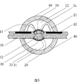
Fig. 3 is the cross-sectional schematic of substrate among the embodiment of the invention 1-4;
Fig. 4 is the structural representation of the embodiment of the invention 1;
Fig. 5 is the structural representation of the embodiment of the invention 2;
Fig. 6 is the structural representation of the embodiment of the invention 3;
Fig. 7 is the schematic top plan view of the embodiment of the invention 4;
Fig. 8 is that the A-A of Fig. 7 is to cutaway view.
Embodiment:
With specific embodiment the present invention is further described below:
Embodiment 1: referring to Fig. 3-4: the light-emitting diode of two-way luminous heat radiation, be the positive and negative electrode on the LED wafer 20 is drawn with lead-in wire 21 respectively and to be connected with lead foot 22 outside extending to lens cap 40, lens cap 40 can cover wafer 20, is fixed with a wafer 20 in the through hole 15 on substrate 10 at least.
Above-mentioned wafer 20 is the wafer of ruddiness or gold-tinted or blue light or green glow or orange light.
The upper and lower side of above-mentioned through hole 15 is the groove 11,12 at the no end of two cup-shapeds that expand outwardly.
Above-mentioned substrate 10 usefulness PCB bases or copper base or aluminium base or iron are made.
Can be provided with cavity 32 between above-mentioned lens cap 40 and the medium 30, in cavity 32, be filled with the inert gas of one of nitrogen, helium, neon, argon gas, xenon.
Above-mentioned lens cap 40 is that the profile of lens cap 40 is circle or ellipse or semicircle or planar shaped or square or honeycomb hexagon with anti-ultraviolet optical glass or optical plastic or resin or silica gel or epoxy resin or ceramic material
Embodiment 2: referring to Fig. 5: basic structure is substantially the same manner as Example 1, when just wafer 20 is the blue light wafer, is provided with printing opacity, heat insulation medium 30 at the outer surface of blue light wafer, and the outer surface of medium 30 or lens cap 40 are provided with layer of fluorescent powder 31.
Above-mentioned medium 30 is to make of heat insulation, printing opacity, anti-ultraviolet silica gel or epoxy resin or pottery or optical plastic or optical glass material.
On fluorescent material 31 be arranged in the interlayer that is arranged on lens cap 40 on the lens cap 40 or the outer surface of the inner surface of lens cap or lens cap or be blended in the material of making lens cap 40.
Embodiment 3: referring to Fig. 6: basic structure is substantially the same manner as Example 2, just, be that above-mentioned layer of fluorescent powder 31 is arranged on the lens cap 40, promptly be arranged in the interlayer of lens cap 40, certainly, above-mentioned fluorescent material is arranged in the interlayer of lens cap or the outer surface of the inner surface of lens cap or lens cap or be blended in the material of making lens cap.
Embodiment 4: referring to Fig. 7-8: the substrate of employing, wafer, bowl-shape recessed cup, medium, inert gas, lead-in wire and lead foot and embodiment 2 or embodiment 3 are basic identical, just a plurality of LED lamp assemblies are installed in the metal case 50, the top and the bottom of box body 50 are all with on anti-ultraviolet optical glass or optical plastic or resin or silica gel or epoxy resin or the ceramic material one-tenth, 41 cappings of lower plane lens cap, in the interlayer of lens cap 41, be respectively arranged with layer of fluorescent powder 31, certainly, also fluorescent material 31 can be arranged on the outer surface of the inner surface of lens cap 41 or lens cap 41 or be blended in the material of making lens cap 41, also can be as embodiment 2, fluorescent material 31 is arranged on the outer surface of medium 30, wafer just, negative electrode is connected in parallel with lead foot respectively with drawing respectively again, certainly, the demand of the quantity of LED how many visual intensities of illumination and designing, because fluorescent material 31 is by medium 30 heat insulation and heat-dissipating space increasings, the good heat dissipation effect of metal case 50, make the stability of LED improve, light efficiency increases, ILS, evidence, the ambient temperature of fluorescent material 31 is low more, its operational environment is just good more, light efficiency is just big more, and the life-span is just long more.
Utilize the light-emitting diode of described two-way luminous heat radiation can produce various luminous class light fixtures such as serial LED illuminating lamp, LED signal lamp, LED light, LED decorative lamp, LED lamp band, LED Lamp cup, LED electricity-saving lamp, LED underground lamp, LED clearance light, LED flood light, can utilize the pin and the external structure of existing light fixture during making, the connection location is gone up structure of the present invention and is got final product, also can redesign and make new-type fitting structure, the different demands that adapt to people are to reach truly energy-saving and cost-reducing.
Claims (10)
1. the light-emitting diode of two-way luminous heat radiation, be the positive and negative electrode on the LED wafer (20) is drawn with lead-in wire (21) respectively and to be connected with lead foot (22) outside extending to lens cap (40,41), lens cap (40,41) can cover wafer (20), it is characterized in that being fixed with a wafer (20) at least in the through hole (15) on substrate (10).
2. the light-emitting diode of two-way luminous heat radiation according to claim 1 is characterized in that the wafer of described wafer (20) for ruddiness or gold-tinted or blue light or green glow or orange light.
3. the light-emitting diode of two-way luminous heat radiation according to claim 1, the upper and lower side that it is characterized in that described through hole (15) is the groove (11,12) at the no end of two cup-shapeds that expand outwardly.
4. the light-emitting diode of two-way luminous heat radiation according to claim 1 is characterized in that described substrate (10) makes with PCB base or copper base or aluminium base or iron.
5. the light-emitting diode of two-way luminous heat radiation according to claim 1, it is characterized in that to be provided with cavity (32) between described lens cap (40,41) and the medium (30), in cavity (32), be filled with the inert gas of one of nitrogen, helium, neon, argon gas, xenon.
6. the light-emitting diode of two-way luminous heat radiation according to claim 1, it is characterized in that described lens cap (40,41) is that the profile of lens cap (40,41) is circle or ellipse or semicircle or planar shaped or square or honeycomb hexagon with anti-ultraviolet optical glass or optical plastic or resin or silica gel or epoxy resin or ceramic material.
7. the light-emitting diode of two-way luminous heat radiation according to claim 1 and 2, the outer surface that it is characterized in that the blue light wafer in described wafer (20) is provided with printing opacity, heat insulation medium (30), and the outer surface of medium (30) or lens cap (40,41) are provided with layer of fluorescent powder (31).
8. the light-emitting diode of two-way luminous heat radiation according to claim 7 is characterized in that described medium (30) is to make of heat insulation, printing opacity, anti-ultraviolet silica gel or epoxy resin or pottery or optical plastic or optical glass material.
9. the light-emitting diode of two-way luminous heat radiation according to claim 7 is characterized in that described fluorescent material (31) is arranged on to be meant in the interlayer that is arranged on lens cap (40,41) on the lens cap (40,41) or the outer surface of the inner surface of lens cap or lens cap or be blended in the material of making lens cap (40,41).
10. the purposes of the light-emitting diode of two-way luminous heat radiation is characterized in that can be used for manufacturing LED illuminating lamp, LED signal lamp, LED light, LED decorative lamp, LED lamp band, LED Lamp cup, LED electricity-saving lamp, LED underground lamp, LED clearance light, LED flood light.
Priority Applications (1)
| Application Number | Priority Date | Filing Date | Title |
|---|---|---|---|
| CNA2007100300608A CN101123289A (en) | 2007-09-05 | 2007-09-05 | Bidirectional luminescent heat radiation LED |
Applications Claiming Priority (1)
| Application Number | Priority Date | Filing Date | Title |
|---|---|---|---|
| CNA2007100300608A CN101123289A (en) | 2007-09-05 | 2007-09-05 | Bidirectional luminescent heat radiation LED |
Publications (1)
| Publication Number | Publication Date |
|---|---|
| CN101123289A true CN101123289A (en) | 2008-02-13 |
Family
ID=39085521
Family Applications (1)
| Application Number | Title | Priority Date | Filing Date |
|---|---|---|---|
| CNA2007100300608A Pending CN101123289A (en) | 2007-09-05 | 2007-09-05 | Bidirectional luminescent heat radiation LED |
Country Status (1)
| Country | Link |
|---|---|
| CN (1) | CN101123289A (en) |
Cited By (13)
| Publication number | Priority date | Publication date | Assignee | Title |
|---|---|---|---|---|
| CN102121689A (en) * | 2010-12-03 | 2011-07-13 | 东莞勤上光电股份有限公司 | Radiating method of LED (light-emitting diode) light source module |
| CN102401255A (en) * | 2011-09-29 | 2012-04-04 | 苏州承源光电科技有限公司 | Spherical LED (light-emitting diode) light source |
| CN102829369A (en) * | 2011-06-17 | 2012-12-19 | 展晶科技(深圳)有限公司 | Light-emitting diode light bar and manufacturing method thereof |
| CN103047575A (en) * | 2011-10-14 | 2013-04-17 | 展晶科技(深圳)有限公司 | Light-emitting diode light bar and manufacture method thereof |
| WO2014012346A1 (en) * | 2012-07-18 | 2014-01-23 | 上海顿格电子贸易有限公司 | Stereoscopic wrapped and encapsulated led chip |
| CN103647014A (en) * | 2013-12-11 | 2014-03-19 | 东莞美盛电器制品有限公司 | Transparent packaging LED light source and manufacturing technology thereof |
| CN101697367B (en) * | 2009-09-30 | 2014-04-02 | 烁光特晶科技有限公司 | Method for preparing LED by using transparent ceramics |
| CN104934516A (en) * | 2014-03-20 | 2015-09-23 | 并日电子科技(深圳)有限公司 | LED package having transparent heat insulation adhesive layer |
| CN106764695A (en) * | 2016-12-30 | 2017-05-31 | 上海升景照明有限公司 | A kind of double-side LED modules suitable for advertising lamp box |
| CN108870158A (en) * | 2018-08-15 | 2018-11-23 | 张辉 | A kind of illuminated LED grid screen display lamp bar of two sided |
| CN112289783A (en) * | 2020-11-26 | 2021-01-29 | 江西瑞晟光电科技有限公司 | LED lamp and packaging process thereof |
| WO2022088293A1 (en) * | 2020-10-29 | 2022-05-05 | 深圳市广社照明科技有限公司 | Remote phosphor large-angle scattering patch led |
| CN115949922A (en) * | 2022-12-26 | 2023-04-11 | 滨海治润电子有限公司 | Novel diode |
-
2007
- 2007-09-05 CN CNA2007100300608A patent/CN101123289A/en active Pending
Cited By (18)
| Publication number | Priority date | Publication date | Assignee | Title |
|---|---|---|---|---|
| CN101697367B (en) * | 2009-09-30 | 2014-04-02 | 烁光特晶科技有限公司 | Method for preparing LED by using transparent ceramics |
| CN102121689B (en) * | 2010-12-03 | 2013-01-02 | 东莞勤上光电股份有限公司 | Radiating method of LED (light-emitting diode) light source module |
| CN102121689A (en) * | 2010-12-03 | 2011-07-13 | 东莞勤上光电股份有限公司 | Radiating method of LED (light-emitting diode) light source module |
| CN102829369A (en) * | 2011-06-17 | 2012-12-19 | 展晶科技(深圳)有限公司 | Light-emitting diode light bar and manufacturing method thereof |
| CN102829369B (en) * | 2011-06-17 | 2014-12-10 | 展晶科技(深圳)有限公司 | Light-emitting diode light bar and manufacturing method thereof |
| CN102401255A (en) * | 2011-09-29 | 2012-04-04 | 苏州承源光电科技有限公司 | Spherical LED (light-emitting diode) light source |
| CN103047575A (en) * | 2011-10-14 | 2013-04-17 | 展晶科技(深圳)有限公司 | Light-emitting diode light bar and manufacture method thereof |
| CN103047575B (en) * | 2011-10-14 | 2015-06-10 | 展晶科技(深圳)有限公司 | Light-emitting diode light bar and manufacture method thereof |
| WO2014012346A1 (en) * | 2012-07-18 | 2014-01-23 | 上海顿格电子贸易有限公司 | Stereoscopic wrapped and encapsulated led chip |
| CN103647014A (en) * | 2013-12-11 | 2014-03-19 | 东莞美盛电器制品有限公司 | Transparent packaging LED light source and manufacturing technology thereof |
| CN104934516A (en) * | 2014-03-20 | 2015-09-23 | 并日电子科技(深圳)有限公司 | LED package having transparent heat insulation adhesive layer |
| CN106764695A (en) * | 2016-12-30 | 2017-05-31 | 上海升景照明有限公司 | A kind of double-side LED modules suitable for advertising lamp box |
| CN108870158A (en) * | 2018-08-15 | 2018-11-23 | 张辉 | A kind of illuminated LED grid screen display lamp bar of two sided |
| CN108870158B (en) * | 2018-08-15 | 2023-11-24 | 张辉 | Double-side-emitting LED grille screen display lamp strip |
| WO2022088293A1 (en) * | 2020-10-29 | 2022-05-05 | 深圳市广社照明科技有限公司 | Remote phosphor large-angle scattering patch led |
| CN112289783A (en) * | 2020-11-26 | 2021-01-29 | 江西瑞晟光电科技有限公司 | LED lamp and packaging process thereof |
| CN115949922A (en) * | 2022-12-26 | 2023-04-11 | 滨海治润电子有限公司 | Novel diode |
| CN115949922B (en) * | 2022-12-26 | 2024-03-01 | 滨海治润电子有限公司 | Novel diode |
Similar Documents
| Publication | Publication Date | Title |
|---|---|---|
| CN201078631Y (en) | White radiation light emitting diode with improved structure | |
| CN101123289A (en) | Bidirectional luminescent heat radiation LED | |
| CN202281062U (en) | LED chip 4-Pi light-emitting LED bulb with high color rendering index | |
| CN101169235A (en) | White light LED with modified structure | |
| CN101769524B (en) | Light emitting diode lamp and light engine thereof | |
| CN101769455A (en) | LED bulb adopting whole-body fluorescence conversion technology | |
| CN201126826Y (en) | Light emitting diode capable of bidirectional luminescence and heat radiation | |
| CN203892915U (en) | Linear LED (light-emitting diode) luminous body and LED lighting lamp | |
| CN101858492A (en) | LED illumination device and application thereof in lamp | |
| CN101737662B (en) | Method for manufacturing integrated packaged high-power LED illuminating light source, and LED illuminating lamp | |
| KR101170992B1 (en) | LED lamp | |
| CN201936915U (en) | LED (light-emitting diode) encapsulating structure and LED module thereof | |
| CN202188416U (en) | Vehicle LED (light-emitting diode) taillight | |
| CN205174069U (en) | LED bulb with U -shaped filament | |
| CN201621627U (en) | Distance separation device for LED and fluorescent powder | |
| CN204756520U (en) | LED fluorescent tube | |
| CN204756519U (en) | LED fluorescent tube | |
| CN203503654U (en) | High-brightness dimmable COB light source | |
| CN104061464B (en) | High-power LED lamp | |
| CN203215372U (en) | High-power LED (light-emitting diode) lamp and radiator for same | |
| CN205824970U (en) | A kind of electricity-saving lamp | |
| TWM332942U (en) | LED with bi-directional shining and heat-radiation | |
| CN205678478U (en) | A kind of can array splicing LED area light source module | |
| CN201517709U (en) | LED lighting lamp | |
| TW200924232A (en) | Light emitting diode capable of radiating light and dissipating heat in dual directions |
Legal Events
| Date | Code | Title | Description |
|---|---|---|---|
| C06 | Publication | ||
| PB01 | Publication | ||
| C10 | Entry into substantive examination | ||
| SE01 | Entry into force of request for substantive examination | ||
| C02 | Deemed withdrawal of patent application after publication (patent law 2001) | ||
| WD01 | Invention patent application deemed withdrawn after publication |
Open date: 20080213 |