CN100543915C - Display panel and display unit - Google Patents
Display panel and display unit Download PDFInfo
- Publication number
- CN100543915C CN100543915C CNB200410099790XA CN200410099790A CN100543915C CN 100543915 C CN100543915 C CN 100543915C CN B200410099790X A CNB200410099790X A CN B200410099790XA CN 200410099790 A CN200410099790 A CN 200410099790A CN 100543915 C CN100543915 C CN 100543915C
- Authority
- CN
- China
- Prior art keywords
- electrode
- fluorescence area
- display panel
- fluorescence
- substrate
- Prior art date
- Legal status (The legal status is an assumption and is not a legal conclusion. Google has not performed a legal analysis and makes no representation as to the accuracy of the status listed.)
- Expired - Fee Related
Links
Images


Classifications
-
- H—ELECTRICITY
- H01—ELECTRIC ELEMENTS
- H01J—ELECTRIC DISCHARGE TUBES OR DISCHARGE LAMPS
- H01J29/00—Details of cathode-ray tubes or of electron-beam tubes of the types covered by group H01J31/00
- H01J29/86—Vessels; Containers; Vacuum locks
- H01J29/89—Optical or photographic arrangements structurally combined or co-operating with the vessel
- H01J29/898—Spectral filters
-
- H—ELECTRICITY
- H01—ELECTRIC ELEMENTS
- H01J—ELECTRIC DISCHARGE TUBES OR DISCHARGE LAMPS
- H01J1/00—Details of electrodes, of magnetic control means, of screens, or of the mounting or spacing thereof, common to two or more basic types of discharge tubes or lamps
- H01J1/02—Main electrodes
- H01J1/30—Cold cathodes, e.g. field-emissive cathode
-
- H—ELECTRICITY
- H01—ELECTRIC ELEMENTS
- H01J—ELECTRIC DISCHARGE TUBES OR DISCHARGE LAMPS
- H01J29/00—Details of cathode-ray tubes or of electron-beam tubes of the types covered by group H01J31/00
- H01J29/02—Electrodes; Screens; Mounting, supporting, spacing or insulating thereof
- H01J29/08—Electrodes intimately associated with a screen on or from which an image or pattern is formed, picked-up, converted or stored, e.g. backing-plates for storage tubes or collecting secondary electrons
- H01J29/085—Anode plates, e.g. for screens of flat panel displays
-
- H—ELECTRICITY
- H01—ELECTRIC ELEMENTS
- H01J—ELECTRIC DISCHARGE TUBES OR DISCHARGE LAMPS
- H01J29/00—Details of cathode-ray tubes or of electron-beam tubes of the types covered by group H01J31/00
- H01J29/02—Electrodes; Screens; Mounting, supporting, spacing or insulating thereof
- H01J29/10—Screens on or from which an image or pattern is formed, picked up, converted or stored
- H01J29/18—Luminescent screens
- H01J29/28—Luminescent screens with protective, conductive or reflective layers
-
- H—ELECTRICITY
- H01—ELECTRIC ELEMENTS
- H01J—ELECTRIC DISCHARGE TUBES OR DISCHARGE LAMPS
- H01J29/00—Details of cathode-ray tubes or of electron-beam tubes of the types covered by group H01J31/00
- H01J29/02—Electrodes; Screens; Mounting, supporting, spacing or insulating thereof
- H01J29/10—Screens on or from which an image or pattern is formed, picked up, converted or stored
- H01J29/18—Luminescent screens
- H01J29/30—Luminescent screens with luminescent material discontinuously arranged, e.g. in dots, in lines
- H01J29/32—Luminescent screens with luminescent material discontinuously arranged, e.g. in dots, in lines with adjacent dots or lines of different luminescent material, e.g. for colour television
Abstract
The invention discloses a kind of display panel with a kind of like this structure, in the display panel of this structure, in the manufacture process of display unit, colour filter unlikely sustains damage because of the heat treatment in reducing atmosphere.Display panel (positive plate AP) comprises the fluorescence area that is formed on the substrate; with the electrode (anode electrode) that is formed on this fluorescence area; this electrode of penetration of electrons that sends from electron source and bump wherein with this fluorescence area; make fluorescence area luminous; to obtain desired images; wherein, begin to form in order colour filter and color filter protecting layer from the side of substrate between substrate and fluorescence area.
Description
The cross reference of related application
The application requires to be submitted on December 26th, 2003 priority of the Japanese priority file No.2003-434348 of Japan Patent office, is incorporated herein this document to do reference.
Technical field
The present invention relates to a kind of display panel and a kind of display unit with colour filter.
Background technology
The display panel that constitutes cold cathode field-emission display device, cathode ray tube or fluorescent display tube (hereinafter many places are referred to as it " display unit " simply) disposes the substrate that comprises glass substrate etc. usually, be formed on the fluorescence area on this substrate and be formed on anode electrode on this fluorescence area.What be provided with between substrate and fluorescence area is colour filter.Material as constituting red color filter for instance, as disclosed among the flat 6-310061 of unexamined Japanese Patent Application Publication specification, generally uses Fe
2O
3Particle.
Patent documentation 1: the flat 6-310061 of unexamined Japanese Patent Application Publication specification
In addition, in the assembling and production process of display unit, in reducing gas atmosphere or deoxidation atmosphere, carry out heat treatment continually.For example, in the production process of cold cathode field-emission display device, have cold-cathode field minus plate that causes radiated element and the positive plate that comprises above-mentioned display panel in order to assemble, (frit glass) couples together the peripheral part of positive plate and the peripheral part of minus plate with glass dust.For they being linked together this glass dust of roasting in reducing gas atmosphere or deoxidation atmosphere (for example in nitrogen atmosphere).
Therefore, in reducing gas atmosphere or deoxidation atmosphere, during the roasting, constitute the Fe of red color filter at glass dust
2O
3Particle is reduced, and perhaps forms Fe
2O
3Oxygen atom be removed (that is) by deoxidation, so red color filter can not normally play a role.
Summary of the invention
Therefore, a task of the present invention provides a kind of display panel with this structure, this structure makes red color filter unlikely sustain damage owing to carry out heat treatment in reducing gas atmosphere or deoxidation atmosphere in the production process of various display unit, and the present invention also provides a kind of display unit that comprises this display panel.
For realizing above-mentioned task; display panel according to first embodiment of the invention is configured to comprise the fluorescence area that is formed on the substrate; with the electrode that is formed on this fluorescence area; wherein bump from electron source electrons emitted through electrode and with fluorescence area; thereby make fluorescence area luminous to obtain desired images; wherein, be formed with colour filter and color filter protecting layer in order from the side of substrate between substrate and fluorescence area.
For realizing above-mentioned task; display panel according to second embodiment of the invention is configured to comprise the fluorescence area that is formed on the substrate; with the electrode that is formed on this fluorescence area; wherein bump from electron source electrons emitted through electrode and with fluorescence area; thereby make fluorescence area luminous to obtain desired images; wherein; electrode comprises a plurality of electrode units; electrode unit and electrode unit are electrically connected mutually by resistive layer, and are formed with colour filter and color filter protecting layer in order from the side of substrate between substrate and fluorescence area.
For realizing above-mentioned task; display panel according to third embodiment of the invention is configured to comprise the fluorescence area that is formed on the substrate; and electrode; wherein bump from electron source electrons emitted and fluorescence area; thereby make fluorescence area luminous to obtain desired images; wherein electrode is formed on the part that does not form fluorescence area on the substrate; and be not formed on the part that is formed with fluorescence area on the substrate, and be formed with colour filter and color filter protecting layer in order from the side of substrate between substrate and fluorescence area.
For realizing above-mentioned task, be configured to comprise according to the display unit of first embodiment of the invention:
(A) minus plate, it has the electron source that is formed on the bearing; With
(B) display panel, it has fluorescence area that is formed on the substrate and the electrode that is formed on this fluorescence area, and wherein bump, thereby make fluorescence area luminous with the acquisition desired images from electron source electrons emitted through electrode and with fluorescence area,
Wherein part around it links together with minus plate and display panel by vacuum layer,
Wherein be formed with colour filter and color filter protecting layer in order from the side of substrate between substrate and fluorescence area.
For realizing above-mentioned task, be configured to comprise according to the display unit of second embodiment of the invention:
(A) minus plate, it has the electron source that is formed on the bearing; With
(B) display panel, it has fluorescence area that is formed on the substrate and the electrode that is formed on this fluorescence area, and wherein bump, thereby make fluorescence area luminous with the acquisition desired images from electron source electrons emitted through electrode and with fluorescence area,
Wherein part around it links together with minus plate and display panel by vacuum layer,
Wherein electrode comprises a plurality of electrode units, and electrode unit and electrode unit are electrically connected mutually by resistive layer,
Wherein be formed with colour filter and color filter protecting layer in order from the side of substrate between substrate and fluorescence area.
For realizing above-mentioned task, be configured to comprise according to the display unit of third embodiment of the invention:
(A) minus plate, it comprises the electron source that is formed on the bearing; With
(B) display panel, it comprises fluorescence area and the electrode that is formed on the substrate, wherein bumps, thereby makes fluorescence area luminous with the acquisition desired images from electron source electrons emitted and fluorescence area,
Wherein part around it links together with minus plate and display panel by vacuum layer,
Wherein electrode is formed on the part that does not form fluorescence area on the substrate, and is not formed on the part that is formed with fluorescence area on the substrate, is formed with colour filter and color filter protecting layer in order from the side of substrate between substrate and fluorescence area.
In the following description, usually be referred to as " first embodiment of the present invention " simply according to the display panel of first embodiment of the invention with according to the display unit of first embodiment of the invention, usually be referred to as " second embodiment of the present invention " simply according to the display panel of second embodiment of the invention with according to the display unit of second embodiment of the invention, usually be referred to as " third embodiment of the present invention " simply according to the display panel of third embodiment of the invention with according to the display unit of third embodiment of the invention.
In the third embodiment of the present invention; in order to protect fluorescence area to make it not be subjected to the damage of ion that the operation because of display unit produces etc. in display unit; in order to suppress to produce gas from fluorescence area; with in order to stop fluorescence area to be eliminated; ideally, on fluorescence area, form the fluorescence diaphragm at least.This fluorescence diaphragm can extend to electrode, and is on the electrode.This fluorescence area is configured to comprise is usually permitted many (a group of a number of) fluorescent grain of one group, and therefore this fluorescence area has uneven surface.Therefore; when the fluorescence diaphragm is formed on the fluorescence area; the fluorescence diaphragm can be a kind of like this state; this state makes part fluorescence diaphragm not contact with the part fluorescence area; perhaps part fluorescence diaphragm is discontinuous state (being formed with a kind of state of depression on part fluorescence diaphragm) on this fluorescence area, and these patterns are included in " being formed with the fluorescence diaphragm on the fluorescence area " this structure.This is applicable to following description.Preferably the fluorescence diaphragm is made up of transparent material.When the fluorescence diaphragm was made up of opaque material, the color of the light that sends from this fluorescence area may be adversely affected.The meaning of term " transparent material " is to have the material of possibility near 100% light transmittance in the visible region.The thickness of fluorescence diaphragm (average thickness of the fluorescence diaphragm on the fluorescence area) is 1 * 10 ideally
-8-1 * 10
-7M is preferably 1 * 10
-8-5 * 10
-8M.The fluorescence diaphragm is preferably by from aluminium nitride (AlN
x), aluminium oxide (Al
2O
3), silica (SiO
x), tin indium oxide (ITO), carborundum (SiC), chromium oxide (CrO
x) and chromium nitride (CrN
x) at least a material selected in the group formed forms, particularly, more preferably by aluminium nitride (AlN
x) form.The example that forms the method for fluorescence diaphragm comprises various physical vapor deposition process (PVD technology), as vacuum deposition processes and sputtering technology and various chemical vapor deposition method (CVD technology).
Electrode can be made up of single electrode (first embodiment of the present invention or the 3rd embodiment) or a plurality of electrode unit (preference pattern of first embodiment of the invention or the 3rd embodiment).For convenience, the preference pattern of the third embodiment of the invention that its electrode is made up of a plurality of electrode units is called " fourth embodiment of the present invention (according to the display panel of fourth embodiment of the invention or according to the display unit of fourth embodiment of the invention) ".When electrode is made up of a plurality of electrode units, must be connected to each other by resistive layer between electrode unit and the electrode unit.The examples of material that constitutes resistive layer comprises material with carbon element, as carborundum (SiC) and SiCN; The SiN material; The refractory metal oxide is as ruthenium-oxide (RuO
2), tantalum oxide, tantalum nitride, chromium oxide and titanium oxide; And semi-conducting material, as amorphous silicon.The sheet resistance of resistive layer can be, for example 1 * 10
-1-1 * 10
10Ω/, preferably 1 * 10
3-1 * 10
8Ω/.The quantity of electrode unit (N) can be 2 or more, and, for instance, when the row of the fluorescence area of arranging in the line add up to n the time, N=n, perhaps (wherein α is greater than or equal to 2 integer to n=α N, be preferably 10≤α≤100, more preferably be 20≤α≤50), perhaps the quantity of electrode unit can be that the quantity at the interval (as described below) that will form with preset distance adds 1 numerical value that obtains, perhaps can equal the quantity of pixel or the quantity of sub-pixel, or near the number the integer corresponding with the quantity of pixel or sub-pixel.Each electrode unit can be identical size, with the location independent of electrode unit, perhaps is of different sizes according to the position of electrode unit is different.
When display unit is colored the demonstration, the row that a row fluorescence area that is arranged in a line can be the row of only being made up of the fluorescence area of red-emitting, the row of only being made up of the fluorescence area of transmitting green light, only is made up of the fluorescence area of emission blue light, perhaps by the fluorescence area of the fluorescence area of continuously arranged red-emitting, transmitting green light, launch the row that the fluorescence area of blue light is formed.This fluorescence area is defined as the fluorescence area that on display panel, forms luminous point.Pixel is made of the group of the fluorescence area of the fluorescence area of the fluorescence area of a red-emitting, a transmitting green light and an emission blue light, and a sub-pixel is made of a fluorescence area (fluorescence area of the fluorescence area of the fluorescence area of a red-emitting, a transmitting green light or an emission blue light).The meaning of the size of the electrode unit corresponding with sub-pixel is the size of surrounding the electrode unit of a fluorescence area.
In the 4th embodiment of the present invention; electrode is made up of a plurality of electrode units; in order to protect fluorescence area to make it not to be subjected to the ion that produces in the display unit or the damage of similar substance; in order to suppress from fluorescence area, to produce gas; with in order to stop fluorescence area to be eliminated; ideally, on fluorescence area, form the fluorescence diaphragm at least.This fluorescence diaphragm can be located on the electrode, on the resistive layer or on electrode and the resistive layer.Ideally, the resistance of fluorescence diaphragm equals or is higher than the resistance of resistive layer, is preferably 10 times of resistive layer resistance or more.The fluorescence diaphragm is preferably by transparent material to be formed.When the fluorescence diaphragm was made up of opaque material, the color of the light that sends from fluorescence area may be adversely affected.The thickness of fluorescence diaphragm (average thickness of the fluorescence diaphragm on the fluorescence area) is 1 * 10 ideally
-8-1 * 10
-7M is preferably 1 * 10
-8-5 * 10
-8M.The fluorescence diaphragm is preferably by from aluminium nitride (AlN
x), aluminium oxide (Al
2O
3), silica (SiO
x), chromium oxide (CrO
x) and chromium nitride (CrN
x) at least a material selected in the group formed forms, particularly, more preferably by aluminium nitride (AlN
x) form.The sheet resistance of fluorescence diaphragm is, for example 1 * 10
6Ω/ or is preferably 1 * 10 more
8Ω/ or more.
In comprising first to fourth embodiment of the present invention of above-mentioned various preference patterns, color filter protecting layer can be selected from the material that can satisfy following condition:
(1) this material has good optical transmission characteristics in the visible region;
(2) this material is stable in the electron beam irradiation;
(3) this material be dense film so that gas can not or porous not basically; With
(4) this material keeps stable when heat treatment or wet process.Especially this colour filter is preferably by from aluminium nitride (AlN
x), chromium nitride (CrN
x), aluminium oxide (AlO
x), chromium oxide (CrO
x), silica (SiO
x), silicon nitride (SiN
x) and silicon oxynitride (SiO
xN
y) at least a material selected in the group formed forms.Can pass through depositing technics, as electron beam deposition technology or hot filament depositing technics; PVD technology such as sputtering technology, ion plating or laser abrasion process; CVD technology; Silk-screen printing technique; Stripping technology (lift-off process); Perhaps sol-gel technology forms color filter protecting layer.
Constitute the material of resistive layer and the example of the combination of the material that constitutes the fluorescence diaphragm and comprise 9 kinds of materials as the examples of material that constitutes resistive layer above-mentioned, i.e. carborundum (SiC), SiCN, SiN material, ruthenium-oxide (RuO
2), tantalum oxide, tantalum nitride, chromium oxide, titanium oxide and amorphous silicon, and 7 kinds of materials as the examples of material that constitutes the fluorescence diaphragm above-mentioned, i.e. aluminium nitride (AlN
x), aluminium oxide (Al
2O
3), silica (SiO
x), tin indium oxide (ITO), carborundum (SiC), chromium oxide (CrO
x) and chromium nitride (CrN
x) combination (9 * 7=63 kind combination) altogether.
Constitute the material of color filter protecting layer and the example of the combination of the material that constitutes resistive layer and comprise that 7 kinds of materials as the examples of material that constitutes color filter protecting layer above-mentioned are aluminium nitride (AlN
x), chromium nitride (CrN
x), aluminium oxide (AlO
x), chromium oxide (CrO
x), silica (SiO
x), silicon nitride (SiN
x) and silicon oxynitride (SiO
xN
y); combination (7 * 9=63 kind combination altogether) with 9 kinds of materials as the examples of material that constitutes resistive layer above-mentioned; and in the middle of this; preferred example as the combination of (constituting the material of colour filter mirror diaphragm)/(constituting the material of resistive layer) can should be mentioned that (aluminium nitride (AlN
x))/(carborundum (SiC)) combination.
The example of combination that constitutes the material of color filter protecting layer and constitute the material of fluorescence diaphragm comprise above-mentioned as the examples of material that constitutes color filter protecting layer 7 kinds of materials and the combination (7 * 7=49 kind combination altogether) of 7 kinds of materials as the examples of material that constitutes the fluorescence diaphragm above-mentioned; and in the middle of this; preferred example as the combination of the material of color filter protecting layer (constitute)/(constituting the material of fluorescence diaphragm) can should be mentioned that (aluminium nitride (AlN
x))/(aluminium nitride (AlN
x)) combination.
In addition; constitute the material of color filter protecting layer; constitute the material of resistive layer and the example of the combination of the material that constitutes the fluorescence diaphragm and comprise 7 kinds of materials as the examples of material that constitutes color filter protecting layer above-mentioned; the combination (7 * 9 * 7=441 kind combination altogether) of 7 kinds of materials of the examples of material that 9 kinds of materials of the examples of material of conduct formation resistive layer above-mentioned and conduct above-mentioned constitute the fluorescence diaphragm; and in the middle of this; preferred example as the combination of the material of color filter protecting layer (constitute)/(constituting the material of resistive layer)/(constituting the material of fluorescence diaphragm) can should be mentioned that (aluminium nitride (AlN
x))/(carborundum (SiC))/(aluminium nitride (AlN
x)) combination.
In the display panel according to the present invention first to the 4th embodiment that comprises above-mentioned various preference patterns, this display panel can constitute the positive plate in the cold cathode field-emission display device, and electrode can constitute the anode electrode in this positive plate.In display unit according to the present invention first to the 4th embodiment that comprises above-mentioned various preference patterns, this display unit can constitute the cold cathode field-emission display device, this display panel can constitute the positive plate in the cold cathode field-emission display device, electrode can constitute the anode electrode in this positive plate, and electron source causes radiated element by cold-cathode field and forms.The example of display unit comprises cathode ray tube (CRT) and fluorescent character display tube, and the example of display panel comprises pole plate and the panel of forming cathode ray tube (CRT) or fluorescent character display tube.
(hereinafter usually be referred to as " the present invention " simply) in the first embodiment of the present invention in the fourth embodiment of the present invention, the example of colour filter comprises red color filter, blue color filter and green color filter.Can pass through, for example, on substrate, form the paste material that (coating) constitutes colour filter earlier, then, for example, this paste material be exposed, develops and drying, to obtain colour filter.As the raw material of red color filter, the example that constitutes the red pigment of this paste material comprises Fe
2O
3, as the raw material of blue color filter, the example that constitutes the blue pigment of this paste material comprises CoOAl
2O
3, as the raw material of green color filter, the example that constitutes the viridine green of this paste material comprises TiO
2NiOCoOZnO and CoOCrOTiO
2Al
2O
3The example that forms the method for paste material membrane comprises spin coating proceeding, silk-screen printing technique and roller coating technology.In addition, the examples of material as constituting colour filter can should be mentioned that so-called dry film (dry film), and in this case, can form colour filter by so-called heat-transferring method.
In the present invention, display panel can have such structure: be formed with many partitions (partition), be used to prevent to produce so-called optical and crosstalk (color muddiness), described optical crosstalk is the electronics in origin autofluorescence zone or enters another fluorescence area from the secondary electron of this fluorescence area emission and cause.
The example of the partition of plane form comprises grid (form of parallel crossed grid), promptly, make this partition surround, the form of all of this fluorescence area four sides for example, wherein this fluorescence area has the basic shape for rectangle (some shape) of the plane form corresponding with sub-pixel, also is included in band shape or strip form that the direction parallel with the opposite side of the fluorescence area that is essentially rectangle or stripe-shaped extended.When partition was grid, partition can have the form of all sides of a fluorescence area of continuous encirclement, perhaps had the form of the side of a fluorescence area of discontinuous encirclement.When partition was band shape or striated, partition can be conitnuous forms or discontinuous form.After forming this partition, can denude so that the end face of partition is smooth partition.
In first embodiment of the present invention, can form color filter protecting layer, make it not exist only on the colour filter, also extend to and be present on the part that does not form colour filter on the substrate.In addition, can form electrode, make it not exist only on the fluorescence area, extend in addition and be present on the part that does not form fluorescence area on the substrate.Especially in first embodiment of the present invention, can obtain electrode by such method, for example in the method, on substrate, form fluorescence area, on this whole surface, form the intermediate coat of forming by polymeric material then, then on this intermediate coat, form conductive material layer, remove this intermediate coat by roasting subsequently.In first embodiment of the present invention, electrode is a sheet, and it covers effective coverage (playing the zone of actual displayed partial action).When forming partition, electrode is formed in this effective coverage, more specifically, is to form towards fluorescence area (comprising the part above the fluorescence area) on the partition.
In first embodiment of the present invention, the order shown in can (A) of following table 1 is produced display panel.Table 1 below in 6, the order of digitized representation step.The meaning of " CF " is a colour filter, the meaning of " formation of electrode unit " is to form electrode unit by conductive material layer of composition, the meaning of " formation of resistive layer " is the formation that is used for the resistive layer that electrode unit is electrically connected between mutually, the meaning of " formation of conductive material layer " is the formation that is used to form the conductive material layer of a plurality of electrode units, and the meaning of " formation of electrode unit " is that the patterning conductive material layer is to obtain the step of electrode unit.
In second embodiment of the present invention, can form color filter protecting layer, make it not exist only on the colour filter, also extend to and be present on the part that does not form colour filter on the substrate.In addition, can form conductive material layer, make it not exist only on the fluorescence area, and extend to and be present on the part that does not form fluorescence area on the substrate.Especially in second embodiment of the present invention, can obtain electrode unit by such method, for example in the method, on substrate, form fluorescence area, on this whole surface, form the intermediate coat of forming by polymeric material then, then on this intermediate coat, form conductive material layer, remove this intermediate coat by roasting subsequently, to obtain flake conductive material layer, this flake conductive material layer of composition then.
In second embodiment of the present invention, when forming partition, preferably the edge of electrode unit (the perhaps edge between electrode unit and the electrode unit) is positioned on the end face of partition, and ideally, resistive layer be formed on the top of the electrode unit that is positioned at least on the partition end face or below so that resistive layer has the part between the edge that places electrode unit.What especially can one carry is, a kind of pattern is that resistive layer is formed on the electrode unit that is positioned on the partition end face, a kind of pattern is that resistive layer is formed on the electrode unit on the top that is positioned at partition end face and partition sidewall and a kind of pattern is that resistive layer is formed on the electrode unit that is positioned on partition end face and the partition sidewall.In addition, what can one carry is, a kind of pattern is that to be formed on the below that is positioned at the electrode unit on the partition end face, a kind of pattern be that below and a kind of pattern of the resistive layer electrode unit that is formed on the side wall upper part that is positioned at partition end face and partition is the below that resistive layer is formed on the electrode unit on the sidewall that is positioned at partition end face and partition to resistive layer.When the material that constitutes resistive layer for from the light of fluorescence area emission when transparent, can form resistive layer and make it extend to and be present in the zone that forms fluorescence area.Resistive layer can be formed by resistance material; and come composition according to photoetching technique and etching technique; select its method according to the material that constitutes resistive layer; mask that perhaps can be by having resistive layer pattern or silk screen are by PVD technology or utilize silk-screen printing technique to form resistance material to obtain resistive layer; also can utilize the oblique incidence vacuum deposition processes, its method is selected according to the shape of partition.
In the second embodiment of the present invention, the order shown in can (B) of following table 1 is made this display panel, and the order shown in the example 3 in (B) of especially preferred following table 1 is made this display panel.
In the third embodiment of the present invention and the 4th embodiment, electrode is formed on the part that does not form fluorescence area on the substrate, and is not formed on the part that is formed with fluorescence area on the substrate.When not forming partition, preferably electrode is formed on the substrate to surround this fluorescence area.On the other hand, when forming partition so that surrounding fluorescence area fully, preferably electrode is formed on the partition and is not formed on the part that is formed with fluorescence area on the substrate.For example, when two opposite side along this fluorescence area form partition, preferably electrode is formed on the partition, and the fluorescence area that is not formed with on the substrate on the part of fluorescence area forms, and is not formed on the part that is formed with fluorescence area on the substrate.Comprise that in the pattern that forms electrode on the partition electrode is formed on pattern on the top that pattern, electrode on the partition end face be formed on partition end face and partition sidewall and electrode and is formed on pattern on partition end face and the partition sidewall.When electrode is made up of a plurality of electrode units (fourth embodiment of the present invention), preferably the edge of electrode unit (the perhaps edge between electrode unit and the electrode unit) is positioned on the end face of partition, and it is desirable to resistive layer be formed on the top of the electrode unit that is positioned at least on the partition end face or below so that resistive layer has the part between the edge that places electrode unit.What especially can one carry is, a kind of pattern, wherein resistive layer is formed on the electrode unit that is positioned on the partition end face, a kind of pattern, wherein resistive layer is formed on the electrode unit on the top that is positioned at partition end face and partition sidewall, with a kind of pattern, wherein resistive layer is formed on the electrode unit that is positioned on partition end face and the partition sidewall.In addition, what can one carry is, a kind of pattern, wherein resistive layer is formed on the below that is positioned at the electrode unit on the partition end face, a kind of pattern, wherein resistive layer is formed on the below of the electrode unit of the side wall upper part that is positioned at partition end face and partition, with a kind of pattern, wherein resistive layer is formed on the below of the electrode unit on the sidewall that is positioned at partition end face and partition.When the material that constitutes resistive layer for from the light of fluorescence area emission when transparent, can form resistive layer and make it extend to and be present in the zone that is formed with fluorescence area.Preferably before forming fluorescence area, form electrode or electrode unit or resistive layer (when forming partition, after forming partition) earlier, but have no particular limits.
In the third embodiment of the present invention and the 4th embodiment, can utilize conductive material layer that electrode or electrode unit are formed on the substrate.Particularly, can obtain electrode or electrode unit, wherein will be formed on the substrate, and come the patterning conductive material layer according to photoetching technique and etching technique by the conductive material layer that electric conducting material constitutes by such method.Selectively; can obtain electrode or electrode unit by so a kind of method; in the method, utilize PVD technology or utilize mask of the pattern of silk-screen printing technique by having electrode or electrode unit or silk screen to form electric conducting material.As the method that forms electrode or electrode unit, more particularly,, can also adopt the oblique incidence vacuum deposition processes according to the form of partition except the method that is used to form the electric conducting material that constitutes electrode or electrode unit cited below.That is, can utilize the oblique incidence vacuum deposition processes only to go up formation electrode or electrode unit at the end face of partition and the sidewall of partition (or top of sidewall).In the fourth embodiment of the present invention, can form resistive layer by similar methods.Specifically; resistive layer can be formed by resistance material; and carry out composition according to photoetching technique and etching technique; perhaps utilize PVD technology or utilize silk-screen printing technique to obtain resistive layer by mask or silk screen formation resistance material with resistive layer pattern; perhaps utilize the oblique incidence vacuum deposition processes, its method will be selected according to the form of partition.
In the third embodiment of the present invention, (C) that can following table 1 or (D) shown in order make this display panel, the order shown in the example 5 in (D) of especially preferred following table 1 is made this display panel.Implement in the example the of the present invention the 4th, can following table 2, the order shown in table 3, table 4, table 5 and the table 6 makes this display panel, example 69 in the especially preferred following table 6 or the order shown in the example 20 in the following table 4 are made this display panel.Be noted that in the third embodiment of the present invention and the 4th embodiment, when color filter protecting layer is made of insulating material, must after forming color filter protecting layer, form electrode or electrode unit again.
Table 1
(A) first embodiment of the present invention
| Example number | The formation of CF | The formation of CF diaphragm | The formation of fluorescence area | The formation of electrode |
| 1 | 1 | 2 | 3 | 4 |
(B) second embodiment of the present invention
| Example number | The formation of CF | The formation of CF diaphragm | The formation of fluorescence area | The formation of electrode unit | The formation of resistive layer |
| 1 | 1 | 2 | 3 | 4 | 5 |
| 2 | 1 | 2 | 3 | 5 | 4 |
| 3 | 2 | 3 | 4 | 5 | 1 |
(C) third embodiment of the present invention (1)
| Example number | The formation of CF | The formation of CF diaphragm | The formation of fluorescence area | The formation of electrode |
| 1 | 1 | 2 | 3 | 4 |
| 2 | 1 | 2 | 4 | 3 |
| 3 | 1 | 3 | 4 | 2 |
| 4 | 2 | 3 | 4 | 1 |
(D) third embodiment of the present invention (2)
| Example number | The formation of CF | The formation of CF diaphragm | The formation of fluorescence area | The formation of electrode | The formation of fluorescence diaphragm |
| 1 | 1 | 2 | 3 | 4 | 5 |
| 2 | 1 | 2 | 3 | 5 | 4 |
| 3 | 1 | 2 | 4 | 3 | 5 |
| 4 | 1 | 3 | 4 | 2 | 5 |
| 5 | 2 | 3 | 4 | 1 | 5 |
Table 2
The fourth embodiment of the present invention (1)
| Example number | The formation of CF | The formation of CF diaphragm | The formation of fluorescence area | The formation of conductive material layer | The formation of electrode unit | The formation of resistive layer |
| 1 | 1 | 2 | 3 | 4 | 5 | 6 |
| 2 | 1 | 2 | 3 | 5 | 6 | 4 |
| 3 | 1 | 2 | 4 | 3 | 5 | 6 |
| 4 | 1 | 2 | 4 | 5 | 6 | 3 |
| 5 | 1 | 2 | 5 | 4 | 6 | 3 |
| 6 | 1 | 2 | 5 | 3 | 4 | 6 |
| 7 | 1 | 2 | 6 | 4 | 5 | 3 |
| 8 | 1 | 2 | 6 | 3 | 4 | 5 |
| 9 | 1 | 3 | 4 | 2 | 5 | 6 |
| 10 | 1 | 3 | 4 | 5 | 6 | 2 |
| 11 | 1 | 3 | 5 | 4 | 6 | 2 |
| 12 | 1 | 3 | 5 | 2 | 4 | 6 |
| 13 | 1 | 3 | 6 | 4 | 5 | 2 |
| 14 | 1 | 3 | 6 | 2 | 4 | 5 |
| 15 | 1 | 4 | 5 | 2 | 3 | 6 |
| 16 | 1 | 4 | 5 | 3 | 6 | 2 |
| 17 | 1 | 4 | 6 | 2 | 3 | 5 |
| 18 | 1 | 4 | 6 | 3 | 5 | 2 |
| 19 | 1 | 5 | 6 | 2 | 3 | 4 |
| 20 | 1 | 5 | 6 | 3 | 4 | 2 |
| 21 | 2 | 3 | 4 | 1 | 5 | 6 |
| 22 | 2 | 3 | 4 | 5 | 6 | 1 |
| 23 | 2 | 3 | 5 | 4 | 6 | 1 |
| 24 | 2 | 3 | 5 | 1 | 4 | 6 |
| 25 | 2 | 3 | 6 | 4 | 5 | 1 |
| 26 | 2 | 3 | 6 | 1 | 4 | 5 |
| 27 | 2 | 4 | 5 | 1 | 3 | 6 |
| 28 | 2 | 4 | 5 | 3 | 6 | 1 |
| 29 | 2 | 4 | 6 | 1 | 3 | 5 |
| 30 | 2 | 4 | 6 | 3 | 5 | 1 |
Table 3
The fourth embodiment of the present invention (2)
| Example number | The formation of CF | The formation of CF diaphragm | The formation of fluorescence area | The formation of conductive material layer | The formation of electrode unit | The formation of |
| 31 | 2 | 5 | 6 | 1 | 3 | 4 |
| 32 | 2 | 5 | 6 | 3 | 4 | 1 |
| 33 | 3 | 4 | 5 | 2 | 6 | 1 |
| 34 | 3 | 4 | 5 | 1 | 2 | 6 |
| 35 | 3 | 4 | 6 | 2 | 5 | 1 |
| 36 | 3 | 4 | 6 | 1 | 2 | 5 |
| 37 | 3 | 5 | 6 | 2 | 4 | 1 |
| 38 | 3 | 5 | 6 | 1 | 2 | 4 |
| 39 | 4 | 5 | 6 | 1 | 2 | 3 |
| 40 | 4 | 5 | 6 | 2 | 3 | 1 |
Table 4
The fourth embodiment of the present invention (3)
| Example number | The formation of CF | The formation of CF diaphragm | The formation of fluorescence area | The formation of conductive material layer | The formation of electrode unit | The formation of resistive layer | The formation of fluorescence diaphragm |
| 1 | 1 | 2 | 3 | 4 | 5 | 6 | 7 |
| 2 | 1 | 2 | 3 | 4 | 5 | 7 | 6 |
| 3 | 1 | 2 | 3 | 4 | 6 | 7 | 5 |
| 4 | 1 | 2 | 3 | 5 | 6 | 4 | 7 |
| 5 | 1 | 2 | 3 | 5 | 6 | 7 | 4 |
| 6 | 1 | 2 | 3 | 5 | 7 | 4 | 6 |
| 7 | 1 | 2 | 3 | 6 | 7 | 5 | 4 |
| 8 | 1 | 2 | 3 | 6 | 7 | 4 | 5 |
| 9 | 1 | 2 | 4 | 3 | 5 | 6 | 7 |
| 10 | 1 | 2 | 4 | 3 | 5 | 7 | 6 |
| 11 | 1 | 2 | 4 | 3 | 6 | 7 | 5 |
| 12 | 1 | 2 | 4 | 5 | 6 | 3 | 7 |
| 13 | 1 | 2 | 4 | 5 | 7 | 3 | 6 |
| 14 | 1 | 2 | 4 | 6 | 7 | 3 | 5 |
| 15 | 1 | 2 | 5 | 4 | 6 | 3 | 7 |
| 16 | 1 | 2 | 5 | 4 | 7 | 3 | 6 |
| 17 | 1 | 2 | 5 | 3 | 4 | 6 | 7 |
| 18 | 1 | 2 | 5 | 3 | 4 | 7 | 6 |
| 19 | 1 | 2 | 6 | 4 | 5 | 3 | 7 |
| 20 | 1 | 2 | 6 | 3 | 4 | 5 | 7 |
| 21 | 1 | 3 | 4 | 2 | 5 | 6 | 7 |
| 22 | 1 | 3 | 4 | 2 | 5 | 7 | 6 |
| 23 | 1 | 3 | 4 | 2 | 6 | 7 | 5 |
| 24 | 1 | 3 | 4 | 5 | 6 | 2 | 7 |
| 25 | 1 | 3 | 4 | 5 | 7 | 2 | 6 |
| 26 | 1 | 3 | 4 | 6 | 7 | 2 | 5 |
| 27 | 1 | 3 | 5 | 4 | 6 | 2 | 7 |
| 28 | 1 | 3 | 5 | 4 | 7 | 2 | 6 |
| 29 | 1 | 3 | 5 | 2 | 4 | 6 | 7 |
| 30 | 1 | 3 | 5 | 2 | 4 | 7 | 6 |
Table 5
The fourth embodiment of the present invention (4)
| Example number | The formation of CF | The formation of CF diaphragm | The formation of fluorescence area | The formation of conductive material layer | The formation of electrode unit | The formation of resistive layer | The formation of |
| 31 | 1 | 3 | 6 | 4 | 5 | 2 | 7 |
| 32 | 1 | 3 | 6 | 2 | 4 | 5 | 7 |
| 33 | 1 | 4 | 5 | 2 | 3 | 6 | 7 |
| 34 | 1 | 4 | 5 | 2 | 3 | 7 | 6 |
| 35 | 1 | 4 | 5 | 3 | 6 | 2 | 7 |
| 36 | 1 | 4 | 5 | 3 | 7 | 2 | 6 |
| 37 | 1 | 4 | 6 | 2 | 3 | 5 | 7 |
| 38 | 1 | 4 | 6 | 3 | 5 | 2 | 7 |
| 39 | 1 | 5 | 6 | 2 | 3 | 4 | 7 |
| 40 | 1 | 5 | 6 | 3 | 4 | 2 | 7 |
| 41 | 2 | 3 | 4 | 1 | 5 | 6 | 7 |
| 42 | 2 | 3 | 4 | 1 | 5 | 7 | 6 |
| 43 | 2 | 3 | 4 | 1 | 6 | 7 | 5 |
| 44 | 2 | 3 | 4 | 5 | 6 | 1 | 7 |
| 45 | 2 | 3 | 4 | 5 | 7 | 1 | 6 |
| 46 | 2 | 3 | 4 | 6 | 7 | 1 | 5 |
| 47 | 2 | 3 | 5 | 4 | 6 | 1 | 7 |
| 48 | 2 | 3 | 5 | 4 | 7 | 1 | 6 |
| 49 | 2 | 3 | 5 | 1 | 4 | 6 | 7 |
| 50 | 2 | 3 | 5 | 1 | 4 | 7 | 6 |
| 51 | 2 | 3 | 6 | 4 | 5 | 1 | 7 |
| 52 | 2 | 3 | 6 | 1 | 4 | 5 | 7 |
| 53 | 2 | 4 | 5 | 1 | 3 | 6 | 7 |
| 54 | 2 | 4 | 5 | 1 | 3 | 7 | 6 |
| 55 | 2 | 4 | 5 | 3 | 6 | 1 | 7 |
| 56 | 2 | 4 | 5 | 3 | 7 | 1 | 6 |
| 57 | 2 | 4 | 6 | 1 | 3 | 5 | 7 |
| 58 | 2 | 4 | 6 | 3 | 5 | 1 | 7 |
| 59 | 2 | 5 | 6 | 1 | 3 | 4 | 7 |
| 60 | 2 | 5 | 6 | 3 | 4 | 1 | 7 |
Table 6
The fourth embodiment of the present invention (5)
| Example number | The formation of CF | The formation of CF diaphragm | The formation of fluorescence area | The formation of conductive material layer | The formation of electrode unit | The formation of resistive layer | The formation of fluorescence diaphragm |
| 61 | 3 | 4 | 5 | 2 | 6 | 1 | 7 |
| 62 | 3 | 4 | 5 | 2 | 7 | 1 | 6 |
| 63 | 3 | 4 | 5 | 1 | 2 | 6 | 7 |
| 64 | 3 | 4 | 5 | 1 | 2 | 7 | 6 |
| 65 | 3 | 4 | 6 | 2 | 5 | 1 | 7 |
| 66 | 3 | 4 | 6 | 1 | 2 | 5 | 7 |
| 67 | 3 | 5 | 6 | 2 | 4 | 1 | 7 |
| 68 | 3 | 5 | 6 | 1 | 2 | 4 | 7 |
| 69 | 4 | 5 | 6 | 1 | 2 | 3 | 7 |
| 70 | 4 | 5 | 6 | 2 | 3 | 1 | 7 |
In the first embodiment of the present invention or second embodiment, the electrode on fluorescence area or the fluorescence area top or the average thickness of electrode unit can be, for example 3 * 10
-8M (30nm)-1.5 * 10
-7M (150nm) is preferably 5 * 10
-8M (50nm)-1 * 10
-7M (100nm).In the third embodiment of the present invention or the 4th embodiment, the electrode on the substrate or the average thickness of electrode unit (when forming partition, the electrode on the end face of partition or the average thickness of electrode unit) can be, for example 3 * 10
-8M (30nm)-1.5 * 10
-7M (150nm) is preferably 5 * 10
-8M (50nm)-1 * 10
-7M (100nm).
In the present invention, the example that constitutes the electric conducting material of electrode (anode electrode) comprises metal, as molybdenum (Mo), aluminium (Al), chromium (Cr), tungsten (W), niobium (Nb), tantalum (Ta), gold (Au), silver (Ag), titanium (Ti), cobalt (Co), zirconium (Zr), iron (Fe), platinum (Pt) and zinc (Zn); (for example, nitride is as TiN, with silicide, as WSi to comprise the alloy of these metallic elements or compound
2, MoSi
2, TiSi
2, and TaSi
2); Semiconductor is as silicon (Si); The carbon film of forming by diamond etc.; With the metal oxide of conduction, as ITO (tin indium oxide), indium oxide and zinc oxide.When forming resistive layer, preferably electrode (anode electrode) is made up of the conductor material of the resistance that does not change resistive layer, and, for example when resistive layer by carborundum (SiC) when forming, preferably electrode (anode electrode) is made up of molybdenum (Mo).
In the present invention, the example of the formation method of the conductive material layer of formation electrode or electrode unit comprises depositing technics, as electron beam deposition technology and hot filament depositing technics; Various PVD technologies are as sputtering technology, ion plating and laser abrasion process; Various CVD technologies; Silk-screen printing technique; Stripping technology; And sol-gel technology.
As the examples of material that constitutes intermediate coat, can mention a kind of lacquer.On broad sense, enamel-cover is drawn together a kind of varnish, as, the main solution of the synthetic that becomes by cellulose derivative group, be generally the nitrocellulose in the solvent flashing, as low-grade fatty acid ester with utilize the urethanes varnish (urethane lacquer) or the acrylic lacquer of another kind of synthetic polymer.When not forming intermediate coat, because the shape on fluorescence area surface makes electrode or the electrode unit on the fluorescence area become uneven, thereby cause that random scatters takes place the electrode or the electrode unit of light on fluorescence area that sends from fluorescence area, so that the defective of the high characteristics of luminescence of display unit can occur to realize.On the other hand, when forming intermediate coat, electrode on the fluorescence area or electrode unit become smoothly, so the electrode on the fluorescence area or electrode unit make the light that sends from fluorescence area reflect in the direction of substrate, thereby can realize the high characteristics of luminescence of display unit.
As the example of the method that forms partition, can mention silk-screen printing technique, dry film method, photoresist process and sand-blast.In the silk-screen printing technique, on a part of silk screen corresponding, has opening with the part that forms partition, the material that allows to utilize blanket cylinder to make and on silk screen, be used to form partition through this opening to form material layer, this material layer is used for forming partition on substrate, roasting is used to form the material layer of partition then.In the dry film method, light-sensitive surface is laminated on the substrate, and makes it exposure, development, thereby remove light-sensitive surface, and fill by removing the film formed opening of sensitization with the material that is used to form partition in the place that will form partition, next carry out roasting.Burn and remove light-sensitive surface by roasting, form partition in the opening thereby the material that forms partition is retained in.In the photoresist process, be formed on the substrate, make it exposure, develop, with the material layer of composition formation partition, roasting then being used to form the photosensitive material layer of having of partition.In the sand-blast, for example, by screen printing or utilize roll coater, blade coating machine, nozzle feeding paint device etc. to make to form the material layer of partition to be formed on the substrate, and make it dry, cover the part of the material layer that is used to form partition then with mask layer, utilize sand-blast to remove the expose portion of the material layer that is used to form partition subsequently.
Angle from the contrast that improves display image preferably, forms the light absorbing zone (black matrix) of an absorption from the light of fluorescence area emission between partition and substrate.As the material that constitutes light absorbing zone, preferential selection can absorb 99% or more material from the light of fluorescence area emission.This examples of material comprises carbon, metallic film (being made of for example chromium, nickel, aluminium, molybdenum or its alloy), metal oxide (for example chromium oxide), metal nitride (for example chromium nitride), heat resistanceheat resistant organic resin, glass cream and comprises black pigment or the glass cream of the conductive particle of silver etc. that concrete example comprises light-sensitive polyimide resin, chromium oxide and chromium oxide/chromium stack membrane.When using chromium oxide/chromium stack membrane, chromium thin film and substrate contacts.Can utilize the method for suitably selecting according to the material that uses, combination as vacuum deposition processes or sputtering technology and etch process, the combination of vacuum deposition processes, sputtering technology or spin coating proceeding and stripping technology, silk-screen printing technique, lithography technique wait and form light absorbing zone.
Fluorescence area can be made of the fluorescent grain of monochromatic fluorescent grain or three kinds of primary colours.The arrangement of fluorescence area can be point-like or striated.In the arrangement of point-like or striated,, can use the gap between the adjacent fluorescence area of light absorbing zone (black matrix) filling in order to improve contrast.
Can be by (for example utilizing by luminous crystalline particle, granular size is the fluorescent grain of 5-10nm) method of the luminous crystalline particle synthetic of preparation forms fluorescence area, in the method, for instance, the luminous crystalline particle synthetic (red fluorescence powder slurry) of red-light-sensing is coated to whole surface, and exposure and development, the fluorescence area that glows with formation, luminous crystalline particle synthetic (green emitting phosphor slurry) with green-light-sensing is coated to whole surface then, and exposure and development, to form the fluorescence area of green light, and then the luminous crystalline particle synthetic (blue colour fluorescent powder slurry) that will feel blue light is coated to whole surface, and exposure and development are to form the fluorescence area of blue light-emitting.The average thickness of fluorescence area but it is desirable to 3-20 μ m without limits on the substrate, is preferably 5-10 μ m.
Fluorescent material as constituting luminous crystalline particle can use a kind of suitable material of selecting from known fluorescent material commonly used.In color monitor, the preferential combination of selecting fluorescent material so that colorimetric purity near the colorimetric purity of three kinds of primary colors stipulating in the NTSC standard, the white balance that obtains when mixing three kinds of primary colors is fabulous, and the duration is short, equates basically between the duration of three kinds of primary colors is mutual.The example that constitutes the fluorescent material of the fluorescence area that glows comprises (Y
2O
3: Eu), (Y
2O
2S:Eu), (Y
3Al
5O
12: Eu), (Y
2SiO
5: Eu) and (Zn
3(PO
4)
2: Mn), and in the middle of these materials, the preferential (Y that uses
2O
3: Eu) with (Y
2O
2S:Eu).The example of the fluorescent material of the fluorescence area of formation green light comprises (ZnSiO2:Mn), (Sr
4Si
3O
8C
14: Eu), (ZnS:Cu, Al), (ZnS:Cu, Au, Al), ((Zn, Cd) S:Cu, Al), (Y
3Al
5O
12: Tb), (Y
2SiO
5: Tb), (Y
3(Al, Ga)
5O
12: Tb), (ZnBaO
4: Mn), (GbBO
3: Tb), (Sr
6SiO
3Cl
3: Eu), (BaMgAl
14O
23: Mn), (ScBO
3: Tb), (Zn
2SiO
4: Mn), (ZnO:Zn), (Gd
2O
2S:Tb) and (ZnGa
2O
4: Mn), and in the middle of these materials, the preferential use (ZnS:Cu, Al), (ZnS:Cu, Au, Al), ((Zn, Cd) S:Cu, Al), (Y
3Al
5O
12: Tb), (Y
3(Al, Ga)
5O
12: Tb) with (Y
2SiO
5: Tb).The example of the fluorescent material of the fluorescence area of formation blue light-emitting comprises (Y
2SiO
5: Ce), (CaWO
4: Pb), CaWO
4, YP
0.85V
0.15O
4, (BaMgAl
14O
23: Eu), (Sr
2P
2O
7: Eu), (Sr
2P
2O
7: Sn), (ZnS:Ag, Al), (ZnS:Ag), ZnMgO and ZnGaO
4, and in the middle of these materials, preferential use (ZnS:Ag) and (ZnS:Ag, Al).
When the cold cathode field-emission display device was made of display unit of the present invention, the cold-cathode field in the cold cathode field-emission display device caused radiated element and (constitutes electron source; Hereinafter, be referred to as " field emission element ") more particularly for example comprise,
(A) cathode electrode, it is formed on the bearing, extends upward in first party,
(B) be formed on insulating barrier on bearing and the cathode electrode;
(C) grid, it is formed on the insulating barrier, extends upward in the second party different with first direction;
(D) be formed on opening portion in grid and the insulating barrier; With
(E) electron emission part that exposes in the opening portion bottom.
Type about the field emission element, have no particular limits, can adopt any in the field emission element of the field emission element of field emission element, platypelloid type of field emission element, the plane of field emission element, the peripheral type of Spindt type and crown type.Cause the angle of radiated element from the cold-cathode field that obtains to have simplified structure, preferred cathode electrode and grid all are striated, and the projected image of the projected image of cathode electrode and grid is orthogonal, and promptly first direction and second direction are orthogonal.
In addition, the field emission element can have focusing electrode.In particular, the field emission element can be the field emission element that further is formed with interlevel dielectric layer and is formed with focusing electrode on grid and insulating barrier on interlevel dielectric layer, or is formed with the field emission element of focusing electrode on the top of grid.Focusing electrode is to make the electrode that focuses on to the track of electrode (anode electrode) electrons emitted from opening portion, and it is luminous or prevent to take place between the neighbor optical crosstalk thereby can improve.In so-called high-pressure type cold cathode field-emission display device, the electrical potential difference between electrode (anode electrode) and the cathode electrode is the magnitude of several kV, and the distance between anode electrode and the cathode electrode is quite big, so focusing electrode is especially effective.The focusing electrode control circuit is applied to relative negative voltage on this focusing electrode.Need on each field emission element, not form focusing electrode, extend to the field emission element and the focusing electrode that exists along the predetermined direction of field emission element arrangements can be produced as the common focusing effect of a plurality of field emission elements.
In the cold cathode field-emission display device, the highfield that is produced by the voltage that is applied on cathode electrode and the grid is applied to electron emission part, makes electronics emit from electron emission part owing to quantum tunneling effect.The electrode (anode electrode) that electronics is formed on the display panel (positive plate) is attracted on the display panel (positive plate), and bumps with fluorescence area.The collision that electronics and fluorescence area take place makes fluorescence area luminous, and described light can be identified as piece image.One or more electron emission part that forms or be arranged in the projected image overlapping areas (overlapping region) of the projected image of cathode electrode and grid constitutes electron emission region.
The example of substrate and bearing comprises the semiconductor substrate that is formed with dielectric film on the quartz base plate that is formed with dielectric film on the glass substrate that is formed with dielectric film on glass substrate, the surface, quartz base plate, the surface and the surface, and, from reducing the angle of production cost, preferentially use the glass substrate that is formed with dielectric film on glass substrate or the surface.The examples of material that is used for glass substrate comprises high strain-point glass, soda-lime glass (Na
2OCaOSiO
2), borosilicate glass (Na
2OB
2O
3SiO
2), forsterite (2MgOSiO
2) and lead glass (Na
2OPbOSiO
2).
The example of the constituent material of cathode electrode, grid and focusing electrode comprises metal, as aluminium (Al), tungsten (W), niobium (Nb), tantalum (Ta), molybdenum (Mo), chromium (Cr), copper (Cu), gold (Au), silver (Ag), titanium (Ti), nickel (Ni), cobalt (Co), zirconium (Zr), iron (Fe), platinum (Pt) and zinc (Zn); (for example, nitride is as TiN, with silicide, as WSi to comprise the alloy of these metallic elements or compound
2, MoSi
2, TiSi
2, and TaSi
2); Semiconductor is as silicon (Si); The carbon film of forming by diamond etc.; With the metal oxide of conduction, as ITO (tin indium oxide), indium oxide and zinc oxide.The example that forms the method for these electrodes comprises the combination of depositing technics (as electron beam deposition technology or hot filament depositing technics, sputtering technology, CVD technology or ion plating and etching), silk-screen printing technique, shikishima plating process (electroplating technology or electroless plating (electroless plating) technology), stripping technology, laser abrasion process and sol-gel technology.For example, can directly form the stripe-shaped electrode by silk-screen printing technique or shikishima plating process.
As the insulating barrier that constitutes the field emission element or the composition material of interlevel dielectric layer, can separately or be used in combination SiO
2Material is as SiO
2, BPSG, PSG, BSG, AsSG, PbSG, SiON, SOG (spin glass, spin on glass), low-melting glass, and glass cream; The SiN material; And insulating resin, as polyimides.When forming insulating barrier or interlevel dielectric layer, can use known technology, as CVD technology, coating processes, sputtering technology, silk-screen printing technique etc.
Can between cathode electrode and electron emission part, form a high resistance membrane.By forming this high resistance membrane, can realize that the cold-cathode field with stable operation and uniform electronic emission characteristics causes radiated element.The examples of material that constitutes high resistance membrane comprises material with carbon element, as carborundum (SiC) and SiCN; The SiN material; Semi-conducting material is as amorphous silicon; With the refractory metal oxide, as ruthenium-oxide (RuO
2), tantalum oxide and tantalum nitride.The example that forms the method for high resistance membrane comprises sputtering technology, CVD technology and silk-screen printing technique.Its resistance is generally 1 * 10
5-1 * 10
7Ω is preferably a few M Ω.
The flat shape (by cut the shape that notch portion obtains open on the imaginary plane parallel with abutment surface) that is formed on the opening portion in grid or the insulating barrier can have any shape, as circle, ellipse, rectangle, polygon, round rectangle (round rectangular form) or fillet polygon (roundpolygonal form).For example can form opening portion with combining of isotropic etching by isotropic etching or anisotropic etching.Selectively, according to the method that forms grid, opening portion can be formed directly in the grid.For example can by isotropic etching or anisotropic etching and isotropic etching combine in insulating barrier or interlevel dielectric layer, form opening portion.
In the cold cathode field-emission display device, the space between positive plate and the minus plate is a vacuum, and therefore when not having dividing plate between positive plate and the minus plate, the cold cathode field-emission display device may be damaged owing to atmospheric pressure.Dividing plate for example can be made of pottery.When this dividing plate was made of pottery, the example of pottery comprised mullite, aluminium oxide, barium titanate, lead zirconate titanate, zirconia, cordierite, borosilicic acid barium, ferrosilite, glass ceramic material and titanium oxide, chromium oxide, iron oxide, vanadium oxide or nickel oxide is joined the material that obtains in these materials.In this case, can produce this dividing plate by making so-called raw sheet (green sheet), firing this raw sheet and cut this raw sheet and fire product.On the surface of dividing plate, can form by conductive material layer, the resistive formation of metal or alloy composition or the thin layer that constitutes by material with low secondary emissionratio.Dividing plate can and be fixed thereon between partition and partition, perhaps can for example form dividing plate support part on the positive plate, and this dividing plate can and be fixed thereon between dividing plate support part and dividing plate support sector branch.
When with positive plate and minus plate when its peripheral part couples together, can use adhesive layer (comprising the glass charge bar), perhaps can be used in combination by the insulation rigid material, the framework that constitutes as glass or pottery links together them.When framework and adhesive layer being combined when using, the distance that obtains when only using adhesive layer is compared, and by the height of suitable Selection Framework, can increase the distance between positive plate and the minus plate.As the composition material of adhesive layer, generally use glass dust, but also can use the so-called low melting point metal material of fusing point with about 120-400 ℃.The example of low melting point metal material comprises In (indium; Fusing point: 157 ℃); The low-melting alloy of indium-Jin; The high-temperature solder of tin (Sn) is as Sn
80Ag
20(fusing point: 220-370 ℃) and Sn
95Cu
5(fusing point: 227-370 ℃); The high-temperature solder of plumbous (Pb) is as Pb
97.5Ag
2.5(fusing point: 304 ℃), Pb
94.5Ag
5.5(fusing point: 304-365 ℃) and Pb
97.5Ag
1.5Sn
1.0(fusing point: 309 ℃); The high melting point solder of zinc (Zn) is as Zn
95Al
5(fusing point: 380 ℃); Tin-plumbous standard solder is as Sn
5Pb
95(fusing point: 300-314 ℃) and Sn
2Pb
98(fusing point: 316-322 ℃); And brazing material, as Au
88Ga
12(fusing point: 381 ℃) (wherein each subscript is represented the percentage of atom).
When substrate, bearing and framework are coupled together, can connect this three assemblies simultaneously, perhaps the first step is that one in substrate and the bearing at first is connected on the framework, in second step another is connected on the framework then.As the example of the gas of forming the atmosphere of using in the connection, can mention nitrogen here.After these three assemblies were coupled together, the space that limited by substrate, bearing, framework and adhesive layer of finding time was to set up vacuum.The atmosphere pressures that is used to connect can or be lower pressure for atmospheric pressure.
Can carry out vacuum exhaust by the chip vacuum tube (chip tube) that is connected in advance on substrate and/or the bearing.The chip vacuum tube generally is made up of glass tube, and the inactive area of utilizing glass dust or above-mentioned low-melting-point metal material to be connected to be formed on substrate and/or bearing (promptly, the periphery of the through hole the part except that being used as the effective coverage of display part), and cut and seal this vacuum tube by heat fused after the arrival of the vacuum degree in this space predetermined value.Because can allow residual gas to enter this space and residual gas is removed from this space,, heat earlier and afterwards cool off whole cold cathode field-emission display device so be preferably before cutting and sealing this chip vacuum tube by vacuum-evacuate operation.
In the cold cathode field-emission display device, cathode electrode is connected to the cathode electrode control circuit, and grid is connected to grid control circuit, and anode electrode is connected on the anode electrode control circuit.These control circuits can be made of known circuit.The output voltage V A of anode electrode control circuit is generally constant, for example can be, 5-10kV.When the distance between positive plate and the minus plate is that (wherein during 0.5mm≤d≤10mm), (unit: value kV/mm) is 0.5-20 to d, is preferably 1-10, is more preferably 5-10 to it is desirable to VA/d.
About voltage VC that is applied to cathode electrode and the voltage VG that is applied to grid, when the working voltage modulation method is controlled method as grade, following pattern is arranged:
(1) a kind of pattern is, the voltage VC that is applied to cathode electrode is a constant, changes the voltage VG that is applied to grid;
(2) a kind of pattern is, changes the voltage VC that is applied to cathode electrode, and the voltage VG that is applied to grid is a constant;
(3) a kind of pattern is, changes the voltage VC that is applied to cathode electrode, also changes the voltage VG that is applied to grid.
In the present invention, form colour filter and color filter protecting layer in this order from the side of substrate between substrate and fluorescence area.That is, colour filter is covered by color filter protecting layer.Therefore, can guarantee that colour filter is without prejudice, described infringement is in the assembling and production process of various display unit, is caused by the heat treatment of carrying out in reducing atmosphere or deoxidation atmosphere.In addition; even when passing fluorescence area from the electron source electrons emitted and bumping with colour filter; can partly divide the material that is deconstructed into colour filter; but the gas that is produced takes place to decompose the material that constitutes colour filter is isolated by colour filter mirror diaphragm, thereby can prevent that gas from having a negative impact to electron source.
In the first embodiment of the present invention or second embodiment,, need the step that forms intermediate coat, on intermediate coat, forms conductive material layer and roasting intermediate coat in order to obtain electrode or a plurality of electrode unit.Therefore, conductive material layer may suffer damage in these steps, or is difficult to reduce the production cost of positive plate.In addition; in order to obtain a plurality of electrode units, necessary dry resistive layer can be removed conductive material layer or fluorescence area in drying steps when forming resistive layer; or in the wet etch operation of the utilization acid that is used for conductive material layer, the fluorescent grain that constitutes fluorescence area can suffer damage.In addition, residue when the resistive layer residue is arranged after removing resistive layer in the assembling and production process of subsequently display unit, may produce gas from the resistive layer residue in heat treatment step.
In the third embodiment of the present invention or the 4th embodiment, electrode is formed on a part of substrate that does not form fluorescence area, and is not formed on a part of substrate that is formed with fluorescence area.In other words, in the third embodiment of the present invention or the 4th embodiment, on fluorescence area, there is no need to form electrode, therefore, do not need to form intermediate coat, on intermediate coat, form the step of conductive material layer and roasting intermediate coat, although this decides according to production technology.Therefore, can prevent that electrode and electrode unit from sustaining damage, thereby can reduce the production cost of display panel or display unit.In addition, when forming resistive layer in order to obtain a plurality of electrode units, by after forming a plurality of electrode units, on substrate, forming fluorescence area, just can not occur in the phenomenon that fluorescence area is removed in the drying steps of resistive layer, and, even when utilizing that for example acid is carried out wet etching to conductive material layer, the fluorescent grain that constitutes fluorescence area can not sustain damage yet.When removing resistive layer, there is not fluorescence area, it is hereby ensured and remove resistive layer, and in the assembling and production process of subsequently display unit, in heat treatment step, can from the resistive layer residue, not produce gas.
In addition, in the third embodiment of the present invention or the 4th embodiment, can reduce the area that the display panel top electrode accounts for, therefore can reduce a kind of capacitor volume of forming by the electrode in the display panel of electron source in the minus plate and display unit, so between display panel and minus plate, can not produce abnormal discharge (vacuum arc discharge).When electrode is made of a plurality of electrode units that are electrically connected by a resistive layer between mutually, can further reduce a kind of capacitor volume of forming by the electrode in the display panel of electron source in the minus plate and display unit (electrode unit), so the just abnormal discharge of more impossible generation (vacuum arc discharge) between display panel and minus plate.In the fourth embodiment of the present invention; when making this display panel, for example, with the order shown in the example 69 in the above-mentioned table 6; utilize a kind of material, can further effectively suppress abnormal discharge of electrode or electrode unit with high-resistance material as the formation color filter protecting layer.
In the third embodiment of the present invention or the 4th embodiment, form electrode and make it surround fluorescence area.Owing to be formed on the electric field that the electrode in the display panel produces, the electron source electrons emitted be attracted on the display panel.In general, slow from electron source to fluorescence area electrons emitted speed.On the other hand, the electronics of close display panel is quickened by the electric field that the electrode that is formed in the display panel produces, so speed is very fast.As a result, electronics moves towards fluorescence area rather than towards electrode, and the collision of electronics and fluorescence area makes fluorescence area luminous, thereby obtains the image that needs.
In the first embodiment of the present invention or second embodiment, electrode is positioned on the fluorescence area, and electrode on the fluorescence area or electrode unit make from the light of fluorescence area emission and reflect in the direction of substrate, thereby obtains the display unit of the high characteristics of luminescence.On the other hand, in the third embodiment of the present invention or the 4th embodiment, by suitably determining the quantity (thickness of fluorescence area on the substrate) of fluorescent grain in the fluorescence area,, also can obtain to have the display panel or the display unit of the high characteristics of luminescence even there is not electrode on the fluorescence area.
Description of drawings
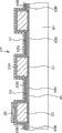
Fig. 1 is the partial side view of the summary of display unit in the example 1 (cold cathode field-emission display device).
Fig. 2 (A) and 2 (B) are the partial side views of the summary of substrate etc., and it explains the manufacture process of display panel in example 1 (constituting the positive plate of cold cathode field-emission display device).
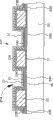
Fig. 3 (A) and 3 (B) are the partial side views of the summary of substrate etc., and it follows the manufacture process that Fig. 2 (B) explains display panel in the example 1 (constituting the positive plate of cold cathode field-emission display device).
Fig. 4 is the partial side view of the summary of substrate etc., and it follows the manufacture process that Fig. 3 (B) explains display panel in the example 1 (constituting the positive plate of cold cathode field-emission display device), the i.e. local enlarged side view of display panel (positive plate) summary in the example 1.
Fig. 5 is the summary fragmentary, perspective view of minus plate in the cold cathode field-emission display device.
Fig. 6 is the view that summary shows the arrangement of partition, dividing plate and fluorescence area in the positive plate that constitutes the cold cathode field-emission display device.
Fig. 7 is the view that summary shows the arrangement of partition, dividing plate and fluorescence area in the positive plate that constitutes the cold cathode field-emission display device.
Fig. 8 is the view that summary shows the arrangement of partition, dividing plate and fluorescence area in the positive plate that constitutes the cold cathode field-emission display device.
Fig. 9 is the view that summary shows the arrangement of partition, dividing plate and fluorescence area in the positive plate that constitutes the cold cathode field-emission display device.
Figure 10 is the view that summary shows the arrangement of partition, dividing plate and fluorescence area in the positive plate that constitutes the cold cathode field-emission display device.
Figure 11 is the view that summary shows the arrangement of partition, dividing plate and fluorescence area in the positive plate that constitutes the cold cathode field-emission display device.
Figure 12 (A) and Figure 12 (B) are the local summary side elevations of bearing etc., and it explains that Spindt type cold-cathode field causes the manufacture process of radiated element.
Figure 13 (A) and Figure 13 (B) are the local summary side elevations of bearing etc., and it is followed Figure 12 (B) and explains that Spindt type cold-cathode field causes the manufacture process of radiated element.
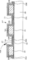
Figure 14 is that summary side elevation is amplified in the part of display panel in the example 2 (positive plate).
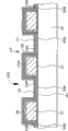
Figure 15 is that summary side elevation is amplified in the part of display panel in the example 3 (positive plate).
Figure 16 is that summary side elevation is amplified in the part of an example of the modification of display panel in the example 3 (positive plate).
Figure 17 is that summary side elevation is amplified in the part of display panel in the example 4 (positive plate).
Figure 18 is that summary side elevation is amplified in the part of an example of the modification of display panel in the example 4 (positive plate).
Figure 19 is that summary side elevation is amplified in the part of display panel in the example 5 (positive plate).
Figure 20 is that summary side elevation is amplified in the part of an example of the modification of display panel in the example 5 (positive plate).
Figure 21 is that summary side elevation is amplified in the part of another example of the modification of display panel in the example 5 (positive plate).
Figure 22 is that summary side elevation is amplified in the part of display panel in the example 6 (positive plate).
Figure 23 is that summary side elevation is amplified in the part of an example of the modification of display panel in the example 6 (positive plate).
Figure 24 is that summary side elevation is amplified in the part of another example of the modification of display panel in the example 6 (positive plate).
Figure 25 is the summary partial side view that Spindt type cold-cathode field with focusing electrode causes radiated element; With
Figure 26 is the summary fragmentary sectional view of so-called two electrode type cold cathode field-emission display devices.
Embodiment
Below, with present invention is described with following Example with reference to the accompanying drawings.
[example 1]
Example 1 relates to according to the display panel of first embodiment of the invention and display unit.More particularly, in example 1, this display unit constitutes the cold cathode field-emission display device, and this display panel constitutes a positive plate in this cold cathode field-emission display device, electrode constitutes the anode electrode in this positive plate, and electron source causes radiated element by a cold-cathode field and constitutes.In the following description, usually abbreviate the cold cathode field-emission display device as " field-emission display device ", display panel is called " positive plate ", electrode is called " anode electrode ", electron source is called " cold-cathode field causes radiated element (field emission element) ".
Fig. 1 shows the summary partial side view of display unit in the example 1; Fig. 4 shows the summary partial side view of display panel in the example 1 (positive plate AP); Fig. 5 shows the summary partial side view of minus plate CP.In addition, the summary part plan of Fig. 6-11 illustrates the example of the arrangement of fluorescence area etc.The arrangement of the fluorescence area in the summary partial side view of positive plate AP etc. and Fig. 7 or shown in Figure 9 corresponding.In Fig. 6-11, electrode (anode electrode) is not shown.
In the field-emission display device of example 1, minus plate CP is connected by vacuum layer at its peripheral part with display panel (positive plate AP).Minus plate CP comprises the electron source (field emission element) that is formed on the bearing 10.On the other hand, display panel (positive plate AP) comprises a plurality of fluorescence area 23 and electrodes (anode electrode 24) that are formed on the substrate 20, the penetration of electrons electrode (anode electrode 24) that sends from electron source (field emission element) and bump wherein with fluorescence area 23, make fluorescence area 23 luminous, thereby obtain desired images.That is to say, field-emission display device in the example 1 comprises minus plate CP, grid 13, electron emission part 15 and positive plate AP, wherein minus plate CP is made of a plurality of field emission elements that all comprise cathode electrode 11, and minus plate CP and positive plate AP link together at its peripheral part.
In the display panel (positive plate AP) of example 1, between fluorescence area on the substrate 20 23 and fluorescence area 23, be formed with black matrix (light absorbing zone) 21.Partition 22 is formed on the black matrix 21.The example of the arrangement of the partition 22 among the positive plate AP, dividing plate 26 and fluorescence area 23 is shown in the view of Fig. 6-11.The example of the plane form of partition 22 comprises grid (parallel criss-cross form), promptly, make partition for example surround the fluorescence area that on plane form be essentially rectangle 23 corresponding with sub-pixel all four limits form (referring to Fig. 6, Fig. 7, Fig. 8 and Fig. 9) and be parallel to the band shape (stripe-shaped) (referring to Figure 10 and Figure 11) that the opposite side of the fluorescence area 23 that is essentially rectangle (or striated) extends.In fluorescence area shown in Figure 10 23, fluorescence area (the fluorescence area 23B of the fluorescence area 23R that glows, the fluorescence area 23G of green light, blue light-emitting) can be the stripe-shaped at longitudinal extension shown in Figure 10.
In example 1, electrode (anode electrode 24) is formed on the whole surface in effective coverage (as the zone of actual displayed part), in particular, is formed on fluorescence area 23 (part that comprises fluorescence area 23 tops) and the partition 22.
Colour filter 30 (30R, 30G, 30B) and color filter protecting layer 31 begin to form in this order from a side that is positioned between substrate 20 and the fluorescence area 23 (23R, 23G, 23B) of substrate.Color filter protecting layer 31 is made of AlNx.
Field emission element shown in Figure 1 is to have the taper electron emission part, the field emission element of promptly so-called spindt type field emission element.This field emission element comprises the cathode electrode 11 that is formed on the bearing 10, be formed on insulating barrier 12 on bearing 10 and the cathode electrode 11, be formed on grid 13 on the insulating barrier 12, be formed on peristome 14 on grid 13 and the insulating barrier 12 (be formed on the first peristome 14A on the grid 13 and be formed on the second peristome 14B on the insulating barrier 12) and be formed on the taper electron emission part 15 of the bottom that is positioned at the second peristome 14B on the cathode electrode 11.In general, cathode electrode 11 and grid 13 are stripe-shaped respectively in one direction, two directions make that the projected image of these electrodes is orthogonal, and a plurality of field emission elements generally are formed in the projected image overlapping areas of two electrodes (with a zone that sub-pixel is corresponding, this zone is overlapping region or electron emission region).In addition, electron emission region is generally arranged with the two-dimensional matrix form in the effective coverage (as the zone of actual displayed part) of minus plate CP.
Sub-pixel is by one group of field emission element of the overlapping region that is formed on the cathode electrode 11 that is arranged in minus plate one side and grid 13, constitutes with fluorescence area 23 (the fluorescence area 23G of a fluorescence area 23R who glows, a green light, the fluorescence area 23B of a blue light-emitting) on the side relative with described one group of field emission element that is positioned at positive plate.In the effective coverage, be arranged with the pixel of hundreds of thousands for example to millions of orders of magnitude.Each pixel is made up of three sub-pixels, and each sub-pixel comprises the fluorescence area 23G of a fluorescence area 23R who glows, a green light or the fluorescence area 23B of a blue light-emitting.
Place positive plate AP and make electron emission region relative, and utilize glass charge bar 25 they to be linked together at peripheral part, to make field-emission display device as adhesive layer with fluorescence area 23 with minus plate CP.The through hole (not shown) that is used for vacuum exhaust is formed on the inactive area of surrounding the effective coverage, and this through hole is connected on the chip vacuum tube (not shown), cuts and seal this chip vacuum tube after exhaust.In other words, the space that is limited by positive plate AP, minus plate CP and glass charge bar 25 is a vacuum, and this space constitutes vacuum layer.Therefore, be applied in atmospheric pressure on positive plate AP and the minus plate CP.In order to prevent that atmospheric pressure from causing damage to field-emission display device, between positive plate AP and minus plate CP, be provided with dividing plate 26.In Fig. 1, this dividing plate is not shown.The part of partition 22 is also supported part as the dividing plate of supporting this dividing plate 26.
Apply relative negative voltage from cathode control circuit 41 to cathode electrode 11, apply relative positive voltage to grid 13, and apply the positive voltage that is higher than the positive voltage that imposes on grid 13 from anode control circuit 43 anode electrodes 24 from grid control circuit 42.When causing emission display then and there and showing, for example, sweep signal inputs to cathode electrode 11 from cathode control circuit 41, and vision signal inputs to grid 13 from grid control circuit 42.Alternatively, conversely, vision signal can input to cathode electrode 11 from cathode control circuit 41, and sweep signal can input to grid 13 from grid control circuit 42.When the part that voltage imposed between cathode electrode 11 and the grid 13, quantum tunneling effect according to the electric field formation that produces, electron emission part 15 is sent electronics, and the electric field that anode electrode 24 forms makes electronics attracted on the positive plate AP, and bump with fluorescence area 23, make fluorescence area 23 be excited and luminous, thereby obtain the image that needs.In other words, the work of this field-emission display device is basically by being applied to the voltage on the grid 13 and being applied to voltage control on the electron emission part 15 by cathode electrode 11.
In example 1, the output voltage V A of anode control circuit 43 is 7kV, and between positive plate and the minus plate is 1mm apart from d, so VA/d=7 (kV/mm of unit).
Below, to be described the display panel (positive plate AP) of example 1 and the manufacture process of display unit (cold cathode field-emission display device) with reference to figure 2 (A) and Fig. 2 (B), Fig. 3 (A) and Fig. 3 (B) and Fig. 4, these accompanying drawings are summary partial side views (referring to the example 1 in (A) of table 1) of substrate etc.
[step-100]
At first, on the substrate 20 that constitutes by glass substrate, form partition 22 (referring to Fig. 2 (A)).The plane form of partition 22 is grid type (a parallel criss-cross form).Specifically, on the whole surface of substrate 20, form the photosensitive polyimide resin layer, make the exposure of photosensitive polyimide resin layer then, develop, with the partition 22 that obtains to have grid (parallel criss-cross form) (referring to, Fig. 7 for example).Selectively, form,, with photoetching technique and etch process this layer of lead glass is optionally handled then, to form partition as the layer of lead glass of cobalt oxide formation black by metal oxide.Also alternatively, can a kind of low-melting glass cream be printed on the substrate 20 by silk-screen printing technique, this low-melting glass cream of roasting forms partition then.The height of the partition 22 in sub-pixel is about 50 μ m.The part of partition is also supported part as the dividing plate of supporting baffle 26.Angle from the contrast that improves display image preferably before forming partition 22, forms black matrix 21 on the part surface of the substrate 20 that will form partition 22 thereon.
[step-110]
Then, for example at first form red color filter 30R.In particular, with a kind of PVA deuterium for chromate photosensitive solution (PVA-deuterated chromate sensitizing solution), as PVA-ADC photosensitive solution or PVA-SDC photosensitive solution, perhaps the azide photosensitive solution (as, polyvinylpyrrolidone) is applied to whole surface, and make it dry, to obtain the photosensitive solution desciccate.Then, utilize unshowned mask with this photosensitive solution desciccate of ultraviolet irradiation, and make it to develop, come to remove the photosensitive solution desciccate from the part substrate 20 that will form red color filter 30R thereon selectively with pure water.Next, the preparation comprise weight ratio be 10% by iron oxide (Fe
2O
3) suspension (residual components is a water) of the red pigment formed of ultramicro powder, this suspension is applied on the whole surface and dry.Then, hydrogen peroxide is sprayed onto on this surface, next,, removes the product and the pigment of unnecessary emulsion drying, thereby obtain red color filter 30R with the product that the pure water discharged-area development should generate.
Then, will be by the PVA deuterium for the CoOAl in the chromate photosensitive solution
2O
3The suspension of the blue pigment that ultramicro powder is formed is applied on this whole surface and makes it dry, then, utilizes unshowned mask with ultraviolet ray it to be shone, and makes it to develop with pure water, obtains blue color filter 30B.Subsequently, will be by the PVA deuterium for the TiO in the chromate photosensitive solution
2The suspension of the viridine green that the ZnOCoONiO ultramicro powder is formed is applied on this whole surface and makes it dry, then, utilize a unshowned mask it to be shone with ultraviolet ray, and make it to develop with pure water, obtain green color filter 30G, thereby obtain the structure shown in Fig. 2 (B).Also can form red color filter 30R in an identical manner.
[step-120]
Next, on whole surface, form color filter protecting layer 31.Exactly, be to utilize sputtering technology on whole surface, to form by AlN
xThe color filter protecting layer of forming 31, thus the structure shown in Fig. 3 (A) obtained.
[step-130]
Next, in order to form the fluorescence area 23R that glows, the fluorescent grain that glows for example is dispersed in polyvinyl alcohol (PVA) resin and water and to wherein adding deuterium for ammonium chromate, obtain a kind of fluorescent powder paste material that glows, this fluorescent powder paste material that glows is applied on the whole surface fluorescent powder paste material drying that this is glowed.Then, will form the part of the fluorescent powder paste material that glows of the fluorescence area 23R that glows on it with ultraviolet irradiation, make the fluorescent powder paste material exposure that glows from the back side one side of substrate 20.This fluorescent powder paste material that glows solidifies gradually from the rear side of substrate 20.The thickness of the fluorescence area 23R that glows that will form is to be determined by the ultraviolet irradiation dosage that shines on the fluorescent powder paste material that glows.Then, the fluorescent powder paste material that glows is developed, between predetermined partition 22, to form the fluorescence area 23R that glows.Next, fluorescent powder paste material to green light is carried out identical processing, to form the fluorescence area 23G of green light, further the fluorescent powder paste material of blue light-emitting is carried out identical processing, with the fluorescence area 23B of formation blue light-emitting, thereby obtain the structure shown in Fig. 3 (B).The thickness of fluorescence area 23 is 3.5-10 μ m.
[step-140]
Then, utilize silk-screen printing technique on whole surface, to form intermediate coat.On broad sense, the resin (lacquer) that constitutes intermediate coat is made up of a kind of varnish, for example, the main solution of the synthetic that becomes by cellulose derivative group, be generally the nitrocellulose in the solvent flashing, as low-grade fatty acid ester, or utilize the urethanes varnish or the acrylic lacquer of another kind of synthetic polymer.Dry then this intermediate coat.
[step-150]
Then, on intermediate coat, form conductive material layer.Specifically, utilize vacuum deposition processes to form the conductive material layer that constitutes by aluminium (Al), thereby cover this intermediate coat.The average thickness of conductive material layer is 0.07 μ m.
[step-160]
Next, at about 400 ℃ of these intermediate coats of following roasting.In calcination process, intermediate coat is burnt, thereby is retained on fluorescence area 23 and the partition 22 by the anode electrode 24 that conductive material layer constitutes.The gas that the intermediate coat roasting produces is discharged by little pore, described little pore for example be formed on conductive material layer in the zone of the shape bending of partition 22.Thereby, can access positive plate AP with structure shown in Figure 4.
[step-170]
Preparation has the minus plate CP of the field emission element of shaping.Assemble field-emission display device then.Specifically, dividing plate 26 is installed on the dividing plate support part in the effective coverage that for example is formed on positive plate AP, arrange positive plate AP and minus plate CP, make fluorescence area 23 relative with the field emission element, and positive plate AP and minus plate CP (substrate 20 and bearing 10 or rather) link together by the glass charge bar 25 as adhesive layer at their peripheral part.In their engaging process, glass charge bar 25 is placed between positive plate AP and the minus plate CP, next this glass charge bar 25 of roasting in deoxidation atmosphere (more particularly, in nitrogen atmosphere).Then, the space that utilizes through hole (not shown) and the emptying of a chip vacuum tube (not shown) to be limited by positive plate AP, minus plate CP and glass charge bar 25 is in case the pressure in this space arrives about 10
-4During Pa, just cut and seal this chip vacuum tube by heat fused.By this way, the space that is limited by positive plate AP, minus plate CP and glass charge bar 25 can become vacuum, thereby obtains field-emission display device as shown in Figure 1.Selectively, according to the structure of this field-emission display device, can utilize by insulation rigid material such as glass or the ceramic framework that constitutes and positive plate AP and minus plate CP is laminated together in conjunction with adhesive layer.Then, connecting up with the external circuit of necessity is connected, thereby just makes this field-emission display device that finishes.
In the example 1, in [step-170], colour filter 30 (especially red color filter 30R) does not suffer damage during the roasting of glass dust.For relatively, omit [step-120], and prepare the positive plate that does not form color filter protecting layer 31, to make field-emission display device.As a result, in [step-170], colour filter 30 (especially red color filter 30R) has been subjected to infringement during the roasting of glass dust.In other words, in deoxidation atmosphere during the roasting glass dust cancellation constitute the Fe of red color filter 30R
2O
3Oxygen atom in the particle (that is), thereby red color filter 30R cisco unity malfunction by deoxidation.
Below, with reference to Figure 12 (A) and 12 (B) and Figure 13 (A) and 13 (B) manufacture process of Spindt type field emission element being described, these figures are the summary partial side view of bearing 10 grades that constitute minus plate.
The method that can form taper electron emission part 15 basically by the vertical evaporation that utilizes metal material obtains Spindt type field emission element.Specifically, evaporating particle enters the first peristome 14A that is formed in the grid 13 in vertical direction, but, near the sedimental screen effect of the external convex type that utilization forms the open end of the first peristome 14A, the quantity that arrives the evaporating particle of second peristome 14B bottom reduces gradually, thereby forms as the sedimental electron emission part 15 of taper in self-adjusting mode.Here, describe a kind of method, in the method, on grid 13 and insulating barrier 12, form peel ply 16 in advance, be used to make and remove unnecessary external convex type deposit and become easy.Accompanying drawing in the manufacture process that is used for explaining the field emission element only shows an electron emission part.
[step-A0]
At first, the conductive material layer of for example being made up of polysilicon that utilizes plasma CVD technology will be used for cathode electrode is deposited on the substrate of being made up of for example glass substrate 10, utilize lithography and dry method etch technology composition to be used for the conductive material layer of cathode electrode then, to form the cathode electrode 11 of stripe-shaped.Utilize CVD technology on whole surface, to form again by SiO
2The insulating barrier of forming 12.
[step-A1]
Next, utilize sputtering technology deposit on insulating barrier 12 to be used for the conductive material layer (for example TiN layer) of grid, utilize lithography and dry etching process composition to be used for the conductive material layer of grid then, to form the grid 13 of stripe-shaped.The cathode electrode 11 of stripe-shaped is extending with the parallel plane direction of accompanying drawing, and the grid 13 of stripe-shaped extends in the direction vertical with the plane of accompanying drawing.
If necessary, can utilize the combination of known film formation method to form grid 13, for instance, PVD technology is as vacuum deposition processes; CVD technology; Shikishima plating process is as electroplating technology or electroless plating technology; Silk-screen printing technique; The laser abrasion process; Sol-gel technology; Perhaps stripping technology, and etching technique.For example, utilize silk-screen printing technique or shikishima plating process can directly form stripe-shaped gate.
[step-A2]
Then, form resistive layer once more, and utilize etching method in grid 13, to form the first peristome 14A, and then in insulating barrier, form the second peristome 14B, thereby make cathode electrode 11 be exposed to the bottom of the second peristome 14B, next remove resistive layer, thereby obtain the structure shown in Figure 12 (A).
[step-A3]
Next, in rotary plate 10, utilize the oblique incidence vacuum deposition processes nickel (Ni) to be deposited on the insulating barrier 12 that comprises grid 13, to form peel ply 16 (referring to Figure 12 (B)).In this case, by the normal with respect to substrate 10 is that evaporating particle (is for example selected enough big incidence angle, 65-85 ° incidence angle), can form peel ply 16 on grid 13 and insulating barrier 12, making does not almost have nickel to be deposited on the bottom of the second peristome 14B.Peel ply 16 is outstanding from the open end of the first peristome 14A as eaves, so reduced the diameter of the first peristome 14A basically.
[step-A4]
Next, for example, will be deposited on the whole surface as the molybdenum (Mo) of conductive materials by vertical evaporation (3-10 ° incidence angle).In this case, shown in Figure 13 (A), because the conductive layer 17 of on peel ply 16, having grown and having dangled shape, so reduced the diameter of the first peristome 14A reality gradually, therefore be used at the evaporating particle that forms deposit on the bottom of the second peristome 14B gradually only by near the center of the first peristome 14A, thereby on the bottom of the second peristome 14B, forming the taper deposit, this taper deposit constitutes electron emission part 15.
[step-A5]
Then, shown in Figure 13 (B), utilize stripping technology to remove peel ply 16, optionally to remove the conductive layer 17 of grid 13 and insulating barrier 12 tops from the surface of grid 13 and insulating barrier 12.Then, in order to expose the open end of grid 13, preferably utilize isotropic etching that the sidewall surfaces that is formed on the second peristome 14B in the insulating barrier 12 is carried out etching.Can be by utilizing the dry etching of atomic group as main etch material, as the chemical drying method etch process or use the wet etching of etching solution to carry out isotropic etching.As etching solution, for example, can use the mixed solution of the 1:100 (volume ratio) of 49% hydrofluoric acid aqueous solution and pure water.Thereby can obtain to be formed with the minus plate of a plurality of Spindt type field emission elements.
[example 2]
Example 2 relates to according to the display panel of second embodiment of the invention and display unit.More particularly, with similar in the example 1, in example 2, this display unit constitutes field-emission display device, this display panel constitutes the positive plate in this field-emission display device, and electrode constitutes the anode electrode in this positive plate, and electron source is made of the field emission element.
Figure 14 shows the summary partial side view that amplify the part of the positive plate AP of the field-emission display device in the configuration example 2.The summary fragmentary, perspective view of minus plate CP and minus plate CP's shown in Figure 5 is similar.In example 2 or routine 3-6 cited below, about the arrangement of fluorescence area etc., for instance, can adopt the arrangement shown in Fig. 6-11, therefore omitted detailed description here.In addition, in example 2 or routine 3-6 cited below, about the structure of the minus plate CP of field-emission display device and the driving method of structure and this field-emission display device, can adopt the structure of minus plate CP of field-emission display device in the example 1 and the driving method of structure and this field-emission display device, therefore omit detailed description here.
In the field-emission display device of example 2, minus plate CP also is connected by vacuum layer at its peripheral part with display panel (positive plate AP).Minus plate CP comprises the electron source (field emission element) that is formed on the bearing 10.Display panel in the example 2 (positive plate AP) also comprises the fluorescence area 23 (23R, 23G, 23B) that is formed on the substrate 20, with the electrode (anode electrode) that is formed on this fluorescence area 23, wherein bump from electron source (field emission element) electrons emitted through electrode (anode electrode) and with fluorescence area 23, make fluorescence area 23 luminous, thereby obtain desired images.Promptly, the field-emission display device of example 2 also comprises minus plate CP and positive plate AP, wherein minus plate CP is made of a plurality of field emission elements that all comprise cathode electrode 11, grid 13, electron emission part 15, and minus plate CP and positive plate AP link together at its peripheral part.This point is applicable to following routine 3-6.
In example 2, colour filter 30 (30R, 30G, 30B) and color filter protecting layer 31 are formed with this order that the side between substrate 20 and the fluorescence area 23 (23R, 23G, 23B) begins that is positioned at from substrate.Color filter protecting layer 31 is by AlN
xConstitute.
In addition, in example 2, electrode (anode electrode) is formed on the inner whole surface, effective coverage (as the zone of actual displayed part), specifically, is formed on fluorescence area 23 (part that comprises fluorescence area 23 tops) and the partition 22.Different with example 1 is that electrode (anode electrode) is made of a plurality of electrode units.In the following description, electrode unit is called " anode electrode unit 24A ".Anode electrode unit 24A and anode electrode unit 24A are electrically connected mutually by resistive layer 28.In example 2, the quantity of anode electrode unit 24A and the quantity of pixel (sub-pixel quantity 1/3) equate, but are not limited to this.
Display panel in the example 2 (positive plate AP) can obtain by a kind of like this method, in the method, after the step identical with [step-160] in the example 1, the patterning conductive material layer is to form groove at a part of conductive material layer that is arranged on partition 22 end faces, obtain anode electrode unit 24A, further on whole surface, form resistive layer 28 then, next the composition resistive layer 28, perhaps can utilize the oblique incidence vacuum deposition processes to obtain resistive layer 28 (referring to the example 1 in the table 1 it (B)).Selectively, can make this display panel (positive plate AP) by a kind of like this method, in the method, after the step identical with [step-130] in the example 1, forming resistive layer on the end face of partition 22 or on the end face of partition 22 and the sidewall, carry out then with example 1 in [step-140] arrive [step-160] identical step, the patterning conductive material layer to be forming groove at a part of conductive material layer that is arranged on partition 22 end faces then, thereby obtains anode electrode unit 24A (referring to the example 2 in the table 1 it (B)).In this case, anode electrode unit 24A places on the resistive layer.
Selectively, can make this display panel (positive plate AP) by a kind of like this method, in the method, after the step identical with [step-100] in the example 1, forming resistive layer on the end face of partition 22 or on the end face of partition 22 and the sidewall, carry out then with example 1 in [step-110] arrive [step-160] identical step, the patterning conductive material layer to be forming groove at a part of conductive material layer that is arranged on partition 22 end faces then, thereby obtains anode electrode unit 24A (referring to the example 3 in the table 1 it (B)).Equally, in this case, anode electrode unit 24A also places on the resistive layer.
In example 2, in the step similar to [step-170], colour filter 30 (especially red color filter 30R) does not suffer damage during the roasting of glass dust.In order to compare, omit and [step-120] similar step, and prepare the positive plate that does not form color filter protecting layer, be used for producing field-emission display device.As a result, in [step-170], colour filter 30 (especially red color filter 30R) has been subjected to infringement during the roasting of glass dust.In other words, in deoxidation atmosphere during the roasting glass dust cancellation constitute the Fe of red color filter 30R
2O
3Oxygen atom in the particle (that is), thereby red color filter 30R cisco unity malfunction by deoxidation.
[example 3]
Example 3 relates to according to a kind of display panel of third embodiment of the invention and a kind of display unit.More particularly, with similar in the example 1, in example 3, this display unit constitutes field-emission display device, this display panel constitutes the positive plate in this field-emission display device, and electrode constitutes the anode electrode in this positive plate, and electron source is made of the field emission element.
Figure 15 or Figure 16 show the summary partial side view that amplify the part of the positive plate AP of the field-emission display device in the configuration example 3.
In example 3, colour filter 30 (30R, 30G, 30B) and color filter protecting layer 31 are formed with this order that the side between substrate 20 and the fluorescence area 23 (23R, 23G, 23B) begins that is positioned at from substrate.Color filter protecting layer 31 is by AlN
xConstitute.
In example 3, electrode (anode electrode 124) is formed on the part that does not form fluorescence area 23 of the interior substrate 20 in effective coverage (as the zone of actual displayed part) (more particularly, be formed on the end face and sidewall of partition 22, be formed in addition on the part that does not form fluorescence area 23 of substrate 20, its midfeather 22 is formed on the substrate 20), and be not formed on a part of 20A of formation fluorescence area 23 of substrate 20.The average thickness of the electrode on partition 22 end faces (anode electrode 124) is 0.1 μ m, and the average thickness of fluorescence area 23 is about 10 μ m.
Can be by the display panel (positive plate AP) (referring to the example 1 in the table 1 it (C)) in the following method manufacturing example 3 shown in Figure 15.
[step-300A]
At first, carry out with example 1 in [step-100] arrive [step-160] identical step.
[step-310A]
Then, the patterning conductive material layer makes to keep to be positioned at the end face of partition 22 and a part of conductive material layer on the sidewall, thereby obtains anode electrode 124 to remove the conductive material layer on the fluorescence area 23.
Can be by the display panel (positive plate AP) (referring to the example 4 in the table 1 it (C)) in the following method manufacturing example 3 shown in Figure 16.
[step-300B]
At first, corresponding to example 1 in [step-100] similar step, form black matrix 21 and partition 22.
[step-310B]
Then, on the part that does not form fluorescence area 23 of substrate 20, form electrode (anode electrode 124).Be noted that electrode is not formed on a part of 20A that will form fluorescence area 23 on the substrate 20.Specifically, utilize the oblique incidence vacuum deposition processes on end face that is formed on the partition 22 on the substrate 20 and sidewall, to form the electrode of forming by conductive material layer (anode electrode 124), electrode (anode electrode 124) is not formed on the part 20A that partition 22 is surrounded on the substrate 20, and wherein this conductive material layer is made of molybdenum (Mo).
[step-320B]
Then, corresponding to example 1 in [step-110] to [step-120] similar step, form colour filter 30 (30R, 30G, 30B) and color filter protecting layer 31.
[step-330B]
Then, corresponding to example 1 in [step-130] similar step, form fluorescence area 23 (23R, 23G, 23B), to obtain the display panel (positive plate AP) in the example shown in Figure 16 3.
Selectively, can come display panel (positive plate AP) in the production example 3 according to the example 2 in the table 1 it (C) or the order of steps shown in the example 3.
[example 4]
Display panel in the example 4 (positive plate) and display unit (cold cathode field-emission display device) are the display panel (positive plate) in the example 3 and the modification of display unit (cold cathode field-emission display device).
Figure 17 or Figure 18 show the summary partial side view that amplify the part of the positive plate AP of the field-emission display device in the configuration example 4.
In the field-emission display device of Fig. 4; in order to protect fluorescence area that it is not subjected to because the operation of field-emission display device and the influence of the ion that in field-emission display device, produces etc.; in order to suppress to produce gas from fluorescence area; with in order to prevent that fluorescence area is eliminated; at least on the fluorescence area 23 (in example 4; more particularly, not only on fluorescence area 23, also on anode electrode 124 as electrode) formed fluorescence diaphragm 27.Fluorescence diaphragm 27 is made of transparent material, specifically by aluminium nitride (AlN
x) constitute.The average thickness of the fluorescence diaphragm 27 on the fluorescence area 23 is 50nm.
Can be by the display panel (positive plate AP) (referring to the example 1 in the table 1 it (D)) in the following method manufacturing example 4 shown in Figure 17.
[step-400A]
At first, carry out with example 1 in [step-100] arrive [step-160] identical step.
[step-410A]
Then, the patterning conductive material layer makes to keep to be positioned at the end face of partition 22 and a part of conductive material layer on the sidewall, thereby obtains anode electrode 124 to remove the conductive material layer on the fluorescence area 23.
[step-420A]
Next, utilize sputtering technology on whole surface, to form by aluminium nitride (AlN
x) the fluorescence diaphragm 27 that constitutes.
Can be by the display panel (positive plate AP) (referring to the example 5 in the table 1 it (D)) in the following method manufacturing example 4 shown in Figure 180.
[step-400B]
At first, carry out with example 3 in [step-300B] arrive [step-330B] identical step.
[step-410B]
Next, utilize sputtering technology on whole surface, to form by aluminium nitride (AlN
x) the fluorescence diaphragm 27 that constitutes.
Some, the display panel in the example 4 (positive plate) is all similar with display unit (cold cathode field-emission display device) with the display panel (positive plate) in the example 3 with display unit (cold cathode field-emission display device) except that above-mentioned, has therefore omitted detailed description.
Selectively, can come display panel (positive plate AP) in the production example 4 according to the order of steps shown in example 2, example 3 or the example 4 in the table 1 it (D).
[example 5]
Display panel in the example 5 (positive plate) and display unit (cold cathode field-emission display device) also are the display panel (positive plate) in the example 3 and the modification of display unit (cold cathode field-emission display device), and relate to display panel and display unit according to fourth embodiment of the invention.
Figure 19, Figure 20 or Figure 21 show the local summary partial side view of amplifying of the positive plate AP of the field-emission display device in the configuration example 5.
In the field-emission display device in example 5, electrode (anode electrode) is made of a plurality of electrode units (anode electrode unit 124A), and anode electrode unit 124A and anode electrode unit 124A are electrically connected mutually by resistive layer 28.In example 5, the quantity of anode electrode unit 124A and the quantity of pixel (equal sub-pixel quantity 1/3) equate, but are not limited to this.
Can be by the display panel (positive plate AP) (referring to the example in the table 2 1) in the following method manufacturing example 5 shown in Figure 19.
[step-500A]
At first, carry out with example 3 in [step-300A] arrive [step-310A] identical step.
[step-510A]
Then, form resistive layer 28 on whole surface, the composition resistive layer 28 then.
Can make the display panel (positive plate AP) (referring to the example in the table 3 36) of example 5 shown in Figure 20 by following method.
[step-500B]
At first, carry out with example 1 in [step-100] identical step.
[step-510B]
Then, utilize the oblique incidence vacuum deposition processes on end face that is formed on the partition 22 on the substrate 20 and sidewall, to form the conductive material layer that constitutes by molybdenum (Mo).Subsequently, (more particularly, being on the conductive material layer that is made of molybdenum) forms protective layer on whole surface, and with this protective layer of photoetching process composition.Then, utilize this patterned protective layer,, remove this protective layer subsequently, thereby obtain anode electrode unit 124A with the conductive material layer that the wet etching process composition is made of molybdenum as etching mask.
[step-520B]
Next, carry out with example 3 in [step-320B] identical step, remove a part of color filter protecting layer 31 that places on partition 22 end faces by composition then, on this part diaphragm, will form resistive layer 28.On whole surface, form resistive layer 28 again, then this resistive layer 28 of composition and the execution step identical with [step-330B].
Can make the display panel (positive plate AP) (referring to the example in the table 3 39) of example 5 shown in Figure 21 by following method.
[step-500C]
At first, execution is arrived [step-510B] identical step with [step-500B].
[step-510C]
Then, utilize the oblique incidence vacuum deposition processes on the anode electrode unit 124A on the sidewall of end face that places partition 22 and partition 22, to form the resistive layer 28 that constitutes by SiC.
[step-520C]
Next, carry out with example 3 in [step-320B] arrive [step-330B] identical step.
Some, the display panel in the example 5 (positive plate) is all similar with display unit (cold cathode field-emission display device) with the display panel (positive plate) in the example 3 with display unit (cold cathode field-emission display device) except that above-mentioned, has therefore omitted detailed description.
Selectively, can come display panel (positive plate AP) in the production example 5 according to the order of steps shown in the example 2-30 in the table 2, example 31-35, example 37, example 38 or the example 40 in the table 3.
[example 6]
Display panel in the example 6 (positive plate) and display unit (cold cathode field-emission display device) are the display panel (positive plate) in the example 5 and the modification of display unit (cold cathode field-emission display device), and relate to display panel and display unit according to the combination of fourth embodiment of the invention especially example 5 and example 4.
Figure 22, Figure 23 or Figure 24 show the local summary partial side view of amplifying of the positive plate AP of the field-emission display device in the configuration example 6.
In the field-emission display device of Fig. 6; in order to protect fluorescence area that it is not subjected to because the operation of emission display is put and influence of putting the ion that produces in the emission display etc. on the scene in the field; in order to suppress to produce gas from fluorescence area; with in order to prevent that fluorescence area is eliminated; at least on the fluorescence area 23 (in example 6; more particularly, not only on fluorescence area 23, also on as the anode electrode 124 of electrode and on resistive layer 28) formed fluorescence diaphragm 27.Fluorescence diaphragm 27 is made of transparent material, specifically by aluminium nitride (AlN
x) constitute.The average thickness of the fluorescence diaphragm 27 on the fluorescence area 23 is 50nm.
Can utilize the display panel (positive plate) in a kind of like this method acquisition example 6, in the method, after the step identical, utilize sputtering technology on whole surface, to form by aluminium nitride (AlN with [step-510A], [step-520B] or [step-520C] in the example 5
x) the fluorescence diaphragm 27 (referring to the example in example in the example in the table 41, the table 6 66 and the table 6 69) that constitutes.
Some, the display panel in the example 6 (positive plate) is all similar with display unit (cold cathode field-emission display device) with the display panel (positive plate) in the example 5 with display unit (cold cathode field-emission display device) except that above-mentioned, has therefore omitted detailed description.
Selectively, can come display panel (positive plate AP) in the production example 6 according to the example 2-30 in the table 4, example 31-60 in the table 5 or the order of steps shown in the example 61-65 in the table 6, example 67, example 68 or the example 70.
Above invention has been described with reference to example, but the present invention is not subjected to the restriction of these examples.The structure and the structure of the display panel of describing in example above (positive plate), minus plate, display unit (cold cathode field-emission display device) and field emission element only are examples, can make suitable change to it.In addition, the production process of positive plate, minus plate, field-emission display device or field emission element also only is example and can makes suitable variation.In addition, the material that uses in the production of positive plate or minus plate also only is example and can makes suitable variation.About field-emission display device, only adopt colored the demonstration, but field-emission display device can be monochromatic the demonstration as an example to its explanation.
In the display panel in example 5 or example 6 (positive plate AP), resistive layer 28 can be formed on the partition 22 between anode electrode unit 124A and the anode electrode unit 124A (promptly between partition 22 and anode electrode unit 124A).
About the field emission element, only the pattern to the corresponding peristome of an electron emission part is illustrated, but, also can adopt the pattern of corresponding peristome of a plurality of electron emission part or the corresponding a plurality of peristomes of electron emission part according to the structure of field emission element.Selectively, can adopt a kind of like this pattern, wherein, in grid, form a plurality of first peristomes, and on insulating barrier, form a plurality of second peristomes that communicate with first peristome, to form one or more electron emission part.
On the scene causing in the radiated element can form interlevel dielectric layer 52, and can form focusing electrode 53 on interlevel dielectric layer 52 on grid 13 and insulating barrier 12.Figure 25 shows the summary partial side view of the field emission element with said structure.In interlevel dielectric layer 52, form the 3rd peristome 54 that communicates with the first peristome 14A.Focusing electrode 53 can adopt a kind of like this method to form, in the method, for example, in [step-A2], on insulating barrier 12, form stripe-shaped gate 13, form interlevel dielectric layer 52 then, on interlevel dielectric layer 52, form patterned focusing electrode 53 subsequently, in focusing electrode 53 and interlevel dielectric layer 52, form the 3rd peristome 54 then, and then in grid 13, form the first peristome 14A.Composition model by the selective focus electrode, focusing electrode can be the form that is made of one group of focusing electrode unit corresponding with or electron emission part or one or more pixel, perhaps is the form that its effective coverage is covered by a sheet of electric conducting material.In Figure 25, show Spindt shape field emission element, but need not explanation, this field emission element can be another kind of type.
Grid can be the type that its effective coverage is covered by a sheet of electric conducting material (having peristome).In this case, positive voltage is applied on this grid.The switch element that is made of for example TFT is formed between the cathode electrode and cathode electrode control circuit that constitutes each pixel, and the action adjustment by switch element is applied to the voltage on the electron emission part that constitutes each pixel, thereby the control pixel is luminous.
Cathode electrode can be the type that its effective coverage is covered by a sheet of electric conducting material.In this case, a voltage is applied on this cathode electrode.A switch element that is made of for example TFT is formed between the electron emission part and grid control circuit that constitutes each pixel, and the action adjustment by switch element is applied to the voltage on the grid that constitutes each pixel, thereby the control pixel is luminous.
The so-called three electrode type cold cathode field-emission display devices that comprise cathode electrode, grid and anode electrode above the cold cathode field-emission display device is not limited to described in example also can be the so-called two electrode type cold cathode field-emission display devices that comprise cathode electrode and anode electrode.Figure 26 shows the summary partial section of an example of the field-emission display device with two electrode type structures, wherein, top structure at the positive plate described in the example 5 is applied in this field-emission display device.In Figure 26, black matrix etc. is not shown.Do not form partition, but it can be formed.Field emission element in this field-emission display device comprises the cathode electrode 11 that is formed on the bearing 10 and is formed on the electron emission part 15A that is made of carbon nano-tube 19 on the cathode electrode 11.Utilize matrix (matrix) 18 that carbon nano-tube 19 is fixed on the surface of cathode electrode 11.The structure of electron emission part is not limited to carbon nano-tube.
The anode electrode that constitutes positive plate AP is made of a plurality of stripe-shaped anode electrode unit 24B.Be not electrically connected between adjacent stripe-shaped anode electrode unit 24B is mutual.In addition, in stripe-shaped anode electrode unit 24B, the conductive material layer that constitutes stripe-shaped anode electrode unit 24B is not formed on the part that is formed with fluorescence area 23 of substrate 20.In other words, in stripe-shaped anode electrode unit 24B, form the fluorescence area 23 of island.The projected image of the projected image of stripe-shaped cathode electrode 11 and stripe-shaped anode electrode unit 24B is orthogonal.More particularly, cathode electrode 11 extends in the direction perpendicular to plane, accompanying drawing place, and stripe-shaped anode electrode unit 24B extends in the direction that is parallel to plane, accompanying drawing place.In the minus plate CP of field-emission display device, many electron emission regions that are made of a plurality of above-mentioned field emission elements are formed in the effective coverage with the form of two-dimensional matrix.
In this field-emission display device, according to quantum tunneling effect, the electric field that anode electrode unit 24B forms makes electronics emit from electron emission part 15A, and electronics attracted on the positive plate AP, bumps with fluorescence area 23.That is to say, with a kind of so-called this field-emission display device of simple matrix mode activated, in this pattern, electronics emits from the electron emission part 15A of the projected image overlapping areas (anode electrode/cathode electrode overlapping region) of the projected image that is arranged in cathode electrode 11 and anode electrode unit 24B.Specifically, relative negative voltage is applied on the cathode electrode 11, relative positive voltage is applied on the anode electrode unit 24B from anode electrode control circuit 43 from cathode electrode control circuit 41.The result, electronics optionally is transmitted into the vacuum space from the carbon nano-tube 19 that constitutes electron emission part 15A, wherein this electron emission part 15A is arranged in selected cathode electrode 11 and selected anode/cathode overlapping region as the anode electrode unit 24B that goes (perhaps selected cathode electrode 11 and selected anode electrode unit 24B as row as row) as row, and electronics attracted on the positive plate AP, bump with the fluorescence area 23 that constitutes positive plate AP, thereby it is luminous to cause fluorescence area 23 to be excited.
Stripe-shaped anode electrode unit 24B can be split into by the interconnected littler anode electrode unit of resistive layer.Specifically, can use the top display panel of in example 6, describing (positive plate AP).Can be in the top cold cathode field-emission display device of in routine 1-4, describing with the structure applications of so-called two electrode types.
In cold cathode field-emission display device of the present invention, the field emission element can be the field emission element of any kind, and as described in the above example, the field emission element not only can for:
(l) Spindt type field emission element, wherein taper electron emission part are formed on the cathode electrode that is positioned at the peristome bottom; In addition can for
(2) platypelloid type field emission element, the electron emission part that wherein is essentially plane are formed on the cathode electrode that is positioned at the peristome bottom;
(3) crown type field emission element, wherein the crown type electron emission part is formed on the cathode electrode that is positioned at peristome bottom, and electronics emits from the coronal of this electron emission part;
(4) plane field emission element, wherein electronics comes out from the surface emitting of flat cathode electrode;
(5) crater (crater) type field emission element, wherein electronics emits from a plurality of protuberances of the uneven surface of cathode electrode; Perhaps
(6) peripheral type field emission element, wherein electronics emits from the marginal portion of cathode electrode.
Except above-described various types of field emission elements, known a kind of element that is called the surface conductance electronic emission element, this element can be applied in the cold cathode field-emission display device of the present invention.In this surface conductance electronic emission element, each all has by a kind of material, as tin oxide (SnO
2), the gold (Au), indium oxide (In
2O
3)/tin oxide (SnO
2), some films in a very little zone constituting of carbon or palladium oxide (PdO) are formed on the substrate that is made of for example glass with matrix form, and each film is made of two films, wherein the circuit of line direction is connected on a slice film, and the circuit of column direction is connected on another sheet film.Between a slice film and another sheet film, be formed with the gap of several nm.In the film selected by the circuit of the circuit of line direction and column direction, electronics emits from this film by the gap.
In Spindt type field emission element, the molybdenum of in example, mentioning above the examples of material that constitutes electron emission part comprises and from by tungsten, tungsten alloy, molybdenum alloy, titanium, titanium alloy, niobium, niobium alloy, tantalum, tantalum alloy, chromium, evanohm with contain at least a material of selecting the group that the silicon of impurity (polysilicon or amorphous silicon) forms.Electron emission part in the Spindt type field emission element can be passed through vacuum deposition processes, and perhaps for example sputtering technology or CVD technology form.
In platypelloid type field emission element, the preferred electron emission part is made of a kind of like this material, the work function Φ of this material is less than the work function of the material that constitutes cathode electrode, and can wait according to electrical potential difference, the required emission between work function, grid and the cathode electrode of the material that constitutes cathode electrode and select this material.The representative example that constitutes the material of the cathode electrode in the field emission element comprises tungsten (Φ=4.55eV), niobium (Φ=4.02-4.87eV), molybdenum (Φ=4.53-4.95eV), aluminium (Φ=4.28eV), copper (Φ=4.6eV), tantalum (Φ=4.3eV), chromium (Φ=4.5eV) and silicon (Φ=4.9eV).Preferably, the work function Φ of electron emission part is less than the work function of above-mentioned material, and its work function is generally 3eV or littler.Such examples of material comprises carbon (Φ<leV), caesium (Φ=2.14eV), LaB
6(Φ=2.66-2.76eV), BaO (Φ=1.6-2.7eV), SrO (Φ=1.25-1.6eV), Y
2O
3(Φ=2.0eV), CaO (Φ=1.6-1.86eV), BaS (Φ=2.05eV), TiN (Φ=2.92eV) and ZrN (Φ=2.92eV).More preferably, electron emission part is that 2eV or littler material constitute by work function Φ.The material that constitutes electron emission part not necessarily has conductive characteristic.
In platypelloid type field emission element, the material that constitutes electron emission part can suitably be selected from the material of its secondary electron gain δ greater than the secondary electron gain δ of the electric conducting material that constitutes cathode electrode.Specifically, can be from metal, as silver (Ag), aluminium (Al), gold (Au), cobalt (Co), copper (Cu), molybdenum (Mo), niobium (Nb), nickel (Ni), platinum (Pt), tantalum (Ta), tungsten (W) and zirconium (Zr); Semiconductor is as silicon (Si) and germanium (Ge); Inorganic simple substance is as carbon and diamond; And compound, as aluminium oxide (Al
2O
3), barium monoxide (BaO), beryllium oxide (BeO), calcium oxide (CaO), magnesium oxide (MgO), tin oxide (SnO
2), barium fluoride (BaF
2) and calcirm-fluoride (CaF
2) in suitably select to constitute the material of electron emission part.The material that constitutes electron emission part not necessarily has conductive characteristic.
In platypelloid type field emission element, the more preferred example that constitutes the material of electron emission part comprises carbon, more particularly diamond, graphite, carbon carbon nano tube structure, ZnO whisker (whisker), MgO whisker, SnO
2Whisker, MnO whisker, Y
2O
3Whisker, NiO whisker, ITO whisker, In
2O
3Whisker and Al
2O
3Whisker.When electron emission part is made of above-mentioned material, can be 5 * 10
7Obtain the emission that the cold cathode field-emission display device needs under V/m or the littler electric field strength.Therefore diamond is a kind of resistance material, can make the emission current that obtains from electron emission part even, thereby the brightness that can suppress in the cold cathode field-emission display device disperses.In addition, these materials have high resistance with respect to the sputter action of the residual gas ion of cold cathode field-emission display device, thereby might prolong the life-span of field emission element.
The object lesson of the structure of carbon nano-tube comprises carbon nano-tube and/or gnf.More particularly, electron emission part can be made of the mixture of carbon nano-tube, gnf or carbon nano-tube and gnf.Carbon nano-tube or gnf can be macroscopic powder or film shape, and if desired, the structure of carbon nano-tube also can be taper.Carbon nano-tube or gnf can produce or form by known arc discharge method, PVD technology such as laser abrasion process or CVD technology such as plasma CVD technology, laser CVD technology, hot CVD technology, gas phase synthesis technique or vapor deposition process.
Also can produce platypelloid type field emission element by a kind of like this method, in the method, with the carbon nano-tube member in the binder material or above-mentioned whisker (hereinafter, it is generically and collectively referred to as simply " carbon nano-tube member etc. ") suspended matter for example be applied in the desired region of cathode electrode, roasting or solidify this binder material (more particularly then, in the method, with organic binder bond material such as epoxy resin or acrylic resin, or the suspended matter of the carbon nano-tube member in inorganic binder material such as the waterglass etc. for example is applied in the desired region of cathode electrode, remove solvent then, next roasting or solidify this binder material).This method is called " first methods of formation carbon nano-tube member etc. ".An example as this coating process can should be mentioned that silk-screen printing technique.
Selectively, can also produce platypelloid type field emission element by a kind of like this method, in the method, the metal compound solution that wherein is suspended with carbon nano-tube member etc. is applied on the cathode electrode, this metallic compound of roasting then is so that utilize the matrix that comprises the metallic atom that constitutes this metallic compound that carbon nano-tube member etc. is fixed on the surface of cathode electrode.This method is called " second methods of formation carbon nano-tube member etc. ".This matrix preferably is made of the metal oxide with conductive characteristic, more particularly, is preferably by tin oxide, indium oxide, tin indium oxide, zinc oxide, antimony oxide or antimony tin and constitutes.After carrying out roasting, can obtain to make the part of each carbon nano-tube member etc. to be embedded into state in the matrix, can obtain perhaps to make that integral body such as each carbon nano-tube member are embedded into the state in the matrix.The specific insulation that it is desirable to matrix is 1 * 10
-9To 5 * 10
-6Ω m.
The example that constitutes the metallic compound of metal compound solution comprises organo-metallic compound, organic acid metal compound and slaine (for example, chloride, nitrate and acetate).Specifically, the example of the metal compound solution that is made of the organic acid metal compound (for example is included in acid, hydrochloric acid, nitric acid or sulfuric acid) in be dissolved with machine tin compound, organic indium compound, organic zinc compound or organo-antimony compound and dilute the solution that this generation solution obtains with organic solvent (for example, toluene, butyl acetate or isopropyl alcohol).Specifically, the example of the metal compound solution that is made of organo-metallic compound is included in the organic solvent (for example, toluene, butyl acetate or isopropyl alcohol) and is dissolved with the solution that machine tin compound, organic indium compound, organic zinc compound or organo-antimony compound obtain.Calculate by weight, comprise 100 parts of metal compound solutions, 0.001-20 part carbon nano-tube member etc. and 0.1-10 part metallic compound preferred the composition.This metal compound solution can comprise a kind of dispersant or a kind of surfactant.In order to increase the thickness of this matrix, a kind of additive can be added, in this metal compound solution as carbon black.If desired, can be used as solvent by water replacement organic solvent.
The example that the metal compound solution that wherein is suspended with carbon nano-tube member etc. is applied to the method on the cathode electrode comprises spraying coating process, spin coating proceeding, dipping process, 1/4th die process (diequarter process) and silk-screen printing technique, in these methods, consider from the easness of operation, preferentially select spraying coating process.
The metal compound solution that wherein is suspended with carbon nano-tube member etc. is applied on the cathode electrode, make the metal compound solution drying to form metal compound layer then, remove the unnecessary portions of the metal compound layer on the cathode electrode again, then can this metallic compound of roasting, perhaps can move unnecessary portions on the cathode electrode behind this metallic compound of roasting, perhaps can only metal compound solution be applied on the desired region of cathode electrode.
The sintering temperature of metallic compound can be a kind of like this temperature, for example, under this temperature, thereby the oxidized metal oxide that forms of slaine with conductive characteristic, perhaps under this temperature, organo-metallic compound or metal salts of organic acids compound decomposition comprise the matrix (metal oxide that for example has conductive characteristic) of the metallic atom that constitutes organo-metallic compound or organic acid metal compound with formation, and this temperature preference is as being 300 ℃ or higher.The upper limit of sintering temperature can be to make the component of field emission element or minus plate not be subjected to the temperature of fire damage or similar damage.
In first method that forms carbon nano-tube member etc. or second method, consider from the angle of the electronic transmitting efficiency of further raising electron emission part, preferably after forming electron emission part, carry out a kind of activation for the surface of electron emission part and handle (clean).The example of this processing is included in the plasma treatment in the atmosphere of hydrogen, ammonia, helium, argon gas, neon, methane gas, ethylene gas, acetylene gas, nitrogen or similar gas.
In first method that forms carbon nano-tube member etc. or second method, electron emission part can be formed on the surface of a part of cathode electrode that is positioned at the peristome bottom, and can form electron emission part so that electron emission part extends to a part of cathode electrode outside the part of peristome bottom from a part of cathode electrode that is positioned at peristome bottom, and be present on its surface.Electron emission part can form wholely or be positioned partially on the surface of a part of cathode electrode of peristome bottom.
Claims (26)
1. display panel, it is configured to comprise the fluorescence area that is formed on the substrate, and electrode, wherein, the electronics and the described fluorescence area that send from electron source bump, and make fluorescence area luminous, obtaining desired images,
Wherein, described electrode is formed on the part that does not form described fluorescence area on the described substrate, and is not formed on the part that is formed with described fluorescence area on the described substrate; And
Begin to be formed with in order colour filter and color filter protecting layer from the side of described substrate between substrate and fluorescence area.
2. display panel as claimed in claim 1, wherein
At least on described fluorescence area, be formed with the fluorescence diaphragm.
3. display panel as claimed in claim 2, wherein
Described fluorescence diaphragm is made of transparent material.
4. display panel as claimed in claim 2, wherein
The thickness of described fluorescence diaphragm is 1 * 10
-8-1 * 10
-7M.
5. display panel as claimed in claim 2, wherein
Described fluorescence diaphragm is made of at least a material of selecting the group of forming from aluminium nitride, aluminium oxide, silica, tin indium oxide, chromium oxide and chromium nitride.
6. display panel as claimed in claim 1, wherein
Described electrode comprises a plurality of electrode units; And
Be electrically connected by resistive layer between described electrode unit is mutual.
7. display panel as claimed in claim 6, wherein
At least on described fluorescence area, be formed with the fluorescence diaphragm.
8. display panel as claimed in claim 7, wherein
The resistance of described fluorescence diaphragm equals or is higher than the resistance of described resistive layer.
9. display panel as claimed in claim 7, wherein
Described fluorescence diaphragm is made of transparent material.
10. display panel as claimed in claim 7, wherein
The thickness of described fluorescence diaphragm is 1 * 10
-8-1 * 10
-7M.
11. display panel as claimed in claim 7, wherein
Described fluorescence diaphragm is made of at least a material of selecting the group of forming from aluminium nitride, aluminium oxide, silica, chromium oxide and chromium nitride.
12. as the described display panel of one of claim 1-11, wherein
Described color filter protecting layer is made of at least a material of selecting the group of forming from aluminium nitride, chromium nitride, aluminium oxide, chromium oxide, silica, silicon nitride and silicon oxynitride.
13. as the described display panel of one of claim 1-11, wherein
Described display panel constitutes the positive plate in the cold cathode field-emission display device; And
Described electrode constitutes the anode electrode in the described positive plate.
14. a display unit, it comprises:
(A) minus plate, it comprises the electron source that is formed on the bearing; With
(B) display panel, it has the fluorescence area that is formed on the substrate, and electrode, and wherein, the electronics and the described fluorescence area that send from described electron source bump, and make described fluorescence area luminous, with the acquisition desired images,
Wherein, described minus plate and described display panel are joined together by vacuum layer in its marginal portion,
Wherein, described electrode is formed on the part that does not form described fluorescence area on the described substrate, and is not formed on the part that is formed with described fluorescence area on the described substrate,
Wherein, begin to be formed with in order colour filter and color filter protecting layer from the side of described substrate between substrate and fluorescence area.
15. display unit as claimed in claim 14, wherein
At least on described fluorescence area, be formed with the fluorescence diaphragm.
16. display unit as claimed in claim 15, wherein
Described fluorescence diaphragm is made of transparent material.
17. display unit as claimed in claim 15, wherein
The thickness of described fluorescence diaphragm is 1 * 10
-8-1 * 10
-7M.
18. display unit as claimed in claim 15, wherein
Described fluorescence diaphragm is made of at least a material of selecting the group of forming from aluminium nitride, aluminium oxide, silica, tin indium oxide, chromium oxide and chromium nitride.
19. display unit as claimed in claim 14, wherein
Described electrode comprises a plurality of electrode units; And
Described electrode unit is electrically connected mutually by resistive layer.
20. display unit as claimed in claim 19, wherein
At least on described fluorescence area, be formed with the fluorescence diaphragm.
21. display unit as claimed in claim 20, wherein
The resistance of described fluorescence diaphragm equals or is higher than the resistance of described resistive layer.
22. display unit as claimed in claim 20, wherein
Described fluorescence diaphragm is made of transparent material.
23. display unit as claimed in claim 20, wherein
The thickness of described fluorescence diaphragm is 1 * 10
-8-1 * 10
-7M.
24. display unit as claimed in claim 20, wherein
Described fluorescence diaphragm is made of at least a material of selecting the group of forming from aluminium nitride, aluminium oxide, silica, tin indium oxide, chromium oxide and chromium nitride.
25. as the described display unit of one of claim 14-24, wherein
Described color filter protecting layer is made of at least a material of selecting the group of forming from aluminium nitride, chromium nitride, aluminium oxide, chromium oxide, silica, silicon nitride and silicon oxynitride.
26. as the described display unit of one of claim 14-24, wherein
Described display panel constitutes the positive plate in the cold cathode field-emission display device; And
Described electrode constitutes the anode electrode in the described positive plate.
Applications Claiming Priority (3)
| Application Number | Priority Date | Filing Date | Title |
|---|---|---|---|
| JP434348/03 | 2003-12-26 | ||
| JP434348/2003 | 2003-12-26 | ||
| JP2003434348A JP4131238B2 (en) | 2003-12-26 | 2003-12-26 | Display panel and display device |
Publications (2)
| Publication Number | Publication Date |
|---|---|
| CN1664980A CN1664980A (en) | 2005-09-07 |
| CN100543915C true CN100543915C (en) | 2009-09-23 |
Family
ID=34545100
Family Applications (1)
| Application Number | Title | Priority Date | Filing Date |
|---|---|---|---|
| CNB200410099790XA Expired - Fee Related CN100543915C (en) | 2003-12-26 | 2004-12-27 | Display panel and display unit |
Country Status (7)
| Country | Link |
|---|---|
| US (1) | US7839063B2 (en) |
| EP (1) | EP1548794B1 (en) |
| JP (1) | JP4131238B2 (en) |
| KR (1) | KR101093837B1 (en) |
| CN (1) | CN100543915C (en) |
| DE (1) | DE602004023683D1 (en) |
| TW (1) | TW200537542A (en) |
Families Citing this family (17)
| Publication number | Priority date | Publication date | Assignee | Title |
|---|---|---|---|---|
| KR20060059617A (en) * | 2004-11-29 | 2006-06-02 | 삼성에스디아이 주식회사 | Flat panel display having spacre and method for fixing spacer of flat panel display |
| CN100530519C (en) * | 2004-12-25 | 2009-08-19 | 鸿富锦精密工业(深圳)有限公司 | Field emission light source and backlight module of using the light source |
| JP4494301B2 (en) * | 2005-07-15 | 2010-06-30 | 株式会社日立製作所 | Image display device |
| KR100708717B1 (en) * | 2005-10-11 | 2007-04-17 | 삼성에스디아이 주식회사 | Light emitting device using electron emission and flat display apparatus using the same |
| KR20070044572A (en) * | 2005-10-25 | 2007-04-30 | 삼성에스디아이 주식회사 | Electron emission display device |
| KR20070046664A (en) * | 2005-10-31 | 2007-05-03 | 삼성에스디아이 주식회사 | Spacer and electron emission display device having the same |
| JP4341609B2 (en) * | 2005-11-02 | 2009-10-07 | ソニー株式会社 | Flat display device and method for manufacturing anode panel in flat display device |
| US7336023B2 (en) * | 2006-02-08 | 2008-02-26 | Youh Meng-Jey | Cold cathode field emission devices having selective wavelength radiation |
| KR20070106231A (en) * | 2006-04-28 | 2007-11-01 | 삼성에스디아이 주식회사 | Composition for preparing electron emitter, method of manufacturing electron emitter using the same, electron emitter and electron emission device manufactured by using this method |
| CN100573797C (en) * | 2006-07-05 | 2009-12-23 | 清华大学 | The field emission pixel tube of double-side |
| FR2917191B1 (en) | 2007-06-11 | 2010-06-11 | Commissariat Energie Atomique | LIGHTING DEVICE FOR LIQUID CRYSTAL DISPLAY |
| JP5264419B2 (en) * | 2008-11-05 | 2013-08-14 | キヤノン株式会社 | Image display device |
| US20120098741A1 (en) * | 2009-06-17 | 2012-04-26 | Industry-University Cooperation Foundation, Hanyang University | Electrophoretic display with integrated touch screen |
| TWI466816B (en) * | 2009-12-30 | 2015-01-01 | Univ Tunghai | Vertically oriented nanowires array structure and method thereof |
| CN103295853B (en) * | 2012-02-23 | 2015-12-09 | 清华大学 | Field emitting electronic source and apply the field emission apparatus of this field emitting electronic source |
| JP5774570B2 (en) * | 2012-11-01 | 2015-09-09 | 双葉電子工業株式会社 | Fluorescent display tube with built-in IC for driving |
| CN111474756B (en) * | 2020-05-27 | 2022-11-08 | 成都中电熊猫显示科技有限公司 | Display panel and method for manufacturing the same |
Family Cites Families (27)
| Publication number | Priority date | Publication date | Assignee | Title |
|---|---|---|---|---|
| JPS6113535A (en) * | 1984-06-28 | 1986-01-21 | Sony Corp | Cathode-ray tube |
| US4857799A (en) * | 1986-07-30 | 1989-08-15 | Sri International | Matrix-addressed flat panel display |
| US5015912A (en) * | 1986-07-30 | 1991-05-14 | Sri International | Matrix-addressed flat panel display |
| JPH06310061A (en) | 1993-02-26 | 1994-11-04 | Sony Corp | Display device |
| JPH0729531A (en) * | 1993-07-12 | 1995-01-31 | Futaba Corp | Fluorescent character display tube |
| JP2809084B2 (en) * | 1994-01-28 | 1998-10-08 | 双葉電子工業株式会社 | Field emission fluorescent display |
| JPH07335141A (en) | 1994-06-06 | 1995-12-22 | Sony Corp | Particulated iron oxide red pigment slurry, its manufacture, and red filter forming method |
| US5508584A (en) * | 1994-12-27 | 1996-04-16 | Industrial Technology Research Institute | Flat panel display with focus mesh |
| FR2732160B1 (en) | 1995-03-22 | 1997-06-13 | Pixtech Sa | RESISTANT STRIP FLAT DISPLAY ANODE |
| KR200147270Y1 (en) * | 1995-06-21 | 1999-06-15 | 손욱 | Crt screen |
| JPH09274103A (en) | 1996-04-04 | 1997-10-21 | Sony Corp | Color filter composition, color display device and its production |
| JP3199682B2 (en) | 1997-03-21 | 2001-08-20 | キヤノン株式会社 | Electron emission device and image forming apparatus using the same |
| JP3943860B2 (en) | 1997-03-21 | 2007-07-11 | キヤノン株式会社 | Image forming apparatus |
| JPH10282330A (en) | 1997-04-10 | 1998-10-23 | Futaba Corp | Manufacture of substrate having color filter, and substrate having color filter |
| JPH10308184A (en) | 1997-05-06 | 1998-11-17 | Hitachi Ltd | Color cathode-ray tube |
| KR20000029597A (en) | 1997-05-26 | 2000-05-25 | 요트.게.아. 롤페즈 | Color display device having color filter layers |
| JPH11185674A (en) * | 1997-12-24 | 1999-07-09 | Futaba Corp | Anode substrate for display tube, and manufacture thereof |
| JPH11213923A (en) | 1998-01-27 | 1999-08-06 | Toshiba Corp | Flat surface display device and manufacture thereof |
| JP2000047190A (en) | 1998-07-31 | 2000-02-18 | Sony Corp | Electro-optic device and its production |
| JP2001195004A (en) | 2000-01-11 | 2001-07-19 | Sony Corp | Flat panel display and method for manufacturing the same as well as color filter |
| JP2002175764A (en) | 2000-12-07 | 2002-06-21 | Sony Corp | Display panel and display device using the same |
| SG118118A1 (en) * | 2001-02-22 | 2006-01-27 | Semiconductor Energy Lab | Organic light emitting device and display using the same |
| US6812636B2 (en) * | 2001-03-30 | 2004-11-02 | Candescent Technologies Corporation | Light-emitting device having light-emissive particles partially coated with light-reflective or/and getter material |
| JP2003177232A (en) * | 2001-10-02 | 2003-06-27 | Seiko Epson Corp | Color filter, method for manufacturing the same, display device and electronic equipment |
| JP2003242911A (en) | 2002-02-20 | 2003-08-29 | Toshiba Corp | Image display device |
| JP2003249165A (en) | 2002-02-26 | 2003-09-05 | Konica Corp | Display substrate, method for manufacturing the same, and display device |
| US6855636B2 (en) * | 2002-10-31 | 2005-02-15 | 3M Innovative Properties Company | Electrode fabrication methods for organic electroluminscent devices |
-
2003
- 2003-12-26 JP JP2003434348A patent/JP4131238B2/en not_active Expired - Fee Related
-
2004
- 2004-12-22 US US11/020,467 patent/US7839063B2/en not_active Expired - Fee Related
- 2004-12-23 EP EP04258076A patent/EP1548794B1/en not_active Expired - Fee Related
- 2004-12-23 TW TW093140307A patent/TW200537542A/en not_active IP Right Cessation
- 2004-12-23 DE DE602004023683T patent/DE602004023683D1/en active Active
- 2004-12-24 KR KR1020040112108A patent/KR101093837B1/en not_active IP Right Cessation
- 2004-12-27 CN CNB200410099790XA patent/CN100543915C/en not_active Expired - Fee Related
Also Published As
| Publication number | Publication date |
|---|---|
| US20050258728A1 (en) | 2005-11-24 |
| KR20050067070A (en) | 2005-06-30 |
| JP2005190960A (en) | 2005-07-14 |
| US7839063B2 (en) | 2010-11-23 |
| CN1664980A (en) | 2005-09-07 |
| EP1548794B1 (en) | 2009-10-21 |
| KR101093837B1 (en) | 2011-12-13 |
| EP1548794A3 (en) | 2005-08-17 |
| TW200537542A (en) | 2005-11-16 |
| DE602004023683D1 (en) | 2009-12-03 |
| TWI316728B (en) | 2009-11-01 |
| EP1548794A2 (en) | 2005-06-29 |
| JP4131238B2 (en) | 2008-08-13 |
Similar Documents
| Publication | Publication Date | Title |
|---|---|---|
| CN100543915C (en) | Display panel and display unit | |
| JP4110912B2 (en) | Cold cathode field emission display | |
| US20050082964A1 (en) | Cold cathode electric field electron emission display device | |
| US20060091780A1 (en) | Flat display device and method for making the same | |
| KR20030001508A (en) | Fluorescent powder, process for producing the same, display panel, and flat display | |
| JP2007005232A (en) | Manufacturing method of anode panel for flat display device, manufacturing method of flat display device, anode panel for flat display device and flat display device | |
| US7329978B2 (en) | Cold cathode field emission display | |
| JP5040081B2 (en) | Flat panel display | |
| JP4305144B2 (en) | Method of assembling a cold cathode field emission display | |
| JP2007027025A (en) | Flat display device, spacer, and manufacturing method of the same | |
| JP5150314B2 (en) | Method for manufacturing anode panel and method for forming phosphor region | |
| JP2005142003A (en) | Display panel and display device | |
| JP4069954B2 (en) | Cold cathode field emission display | |
| JP4140657B2 (en) | Cold cathode field emission display | |
| JP2005004971A (en) | Flat display device and its assembly method | |
| JP5345324B2 (en) | Cold cathode field emission display | |
| JP4466496B2 (en) | Spacer and flat display device | |
| JP4844041B2 (en) | Cathode panel for cold cathode field emission display and cold cathode field emission display | |
| JP4228968B2 (en) | Cathode panel for cold cathode field emission display and cold cathode field emission display | |
| JP2009170280A (en) | Cold cathode field electron emission element manufacturing method and cold cathode field electron emission display device manufacturing method | |
| JP2008004280A (en) | Flat panel display device | |
| JP2009218142A (en) | Method of manufacturing anode panel | |
| KR20060136318A (en) | Method of manufacturing anode panel for flat-panel display device, method of manufacturing flat-panel display device, anode panel for flat-panel display device, and flat-panel display device | |
| JP2008066313A (en) | Cold cathode field electron emission display device | |
| JP2004165001A (en) | Manufacturing method of flat display device |
Legal Events
| Date | Code | Title | Description |
|---|---|---|---|
| C06 | Publication | ||
| PB01 | Publication | ||
| C10 | Entry into substantive examination | ||
| SE01 | Entry into force of request for substantive examination | ||
| C14 | Grant of patent or utility model | ||
| GR01 | Patent grant | ||
| C17 | Cessation of patent right | ||
| CF01 | Termination of patent right due to non-payment of annual fee |
Granted publication date: 20090923 Termination date: 20131227 |