CN100520900C - Method for operating active-matrix display - Google Patents
Method for operating active-matrix display Download PDFInfo
- Publication number
- CN100520900C CN100520900C CNB2006101014098A CN200610101409A CN100520900C CN 100520900 C CN100520900 C CN 100520900C CN B2006101014098 A CNB2006101014098 A CN B2006101014098A CN 200610101409 A CN200610101409 A CN 200610101409A CN 100520900 C CN100520900 C CN 100520900C
- Authority
- CN
- China
- Prior art keywords
- type display
- active matrix
- matrix type
- video signal
- control information
- Prior art date
- Legal status (The legal status is an assumption and is not a legal conclusion. Google has not performed a legal analysis and makes no representation as to the accuracy of the status listed.)
- Expired - Lifetime
Links
Images


Classifications
-
- G—PHYSICS
- G09—EDUCATION; CRYPTOGRAPHY; DISPLAY; ADVERTISING; SEALS
- G09G—ARRANGEMENTS OR CIRCUITS FOR CONTROL OF INDICATING DEVICES USING STATIC MEANS TO PRESENT VARIABLE INFORMATION
- G09G3/00—Control arrangements or circuits, of interest only in connection with visual indicators other than cathode-ray tubes
- G09G3/006—Electronic inspection or testing of displays and display drivers, e.g. of LED or LCD displays
-
- G—PHYSICS
- G09—EDUCATION; CRYPTOGRAPHY; DISPLAY; ADVERTISING; SEALS
- G09G—ARRANGEMENTS OR CIRCUITS FOR CONTROL OF INDICATING DEVICES USING STATIC MEANS TO PRESENT VARIABLE INFORMATION
- G09G3/00—Control arrangements or circuits, of interest only in connection with visual indicators other than cathode-ray tubes
- G09G3/20—Control arrangements or circuits, of interest only in connection with visual indicators other than cathode-ray tubes for presentation of an assembly of a number of characters, e.g. a page, by composing the assembly by combination of individual elements arranged in a matrix no fixed position being assigned to or needed to be assigned to the individual characters or partial characters
- G09G3/34—Control arrangements or circuits, of interest only in connection with visual indicators other than cathode-ray tubes for presentation of an assembly of a number of characters, e.g. a page, by composing the assembly by combination of individual elements arranged in a matrix no fixed position being assigned to or needed to be assigned to the individual characters or partial characters by control of light from an independent source
- G09G3/36—Control arrangements or circuits, of interest only in connection with visual indicators other than cathode-ray tubes for presentation of an assembly of a number of characters, e.g. a page, by composing the assembly by combination of individual elements arranged in a matrix no fixed position being assigned to or needed to be assigned to the individual characters or partial characters by control of light from an independent source using liquid crystals
- G09G3/3611—Control of matrices with row and column drivers
- G09G3/3648—Control of matrices with row and column drivers using an active matrix
-
- H—ELECTRICITY
- H04—ELECTRIC COMMUNICATION TECHNIQUE
- H04N—PICTORIAL COMMUNICATION, e.g. TELEVISION
- H04N17/00—Diagnosis, testing or measuring for television systems or their details
- H04N17/04—Diagnosis, testing or measuring for television systems or their details for receivers
-
- H—ELECTRICITY
- H04—ELECTRIC COMMUNICATION TECHNIQUE
- H04N—PICTORIAL COMMUNICATION, e.g. TELEVISION
- H04N5/00—Details of television systems
- H04N5/66—Transforming electric information into light information
-
- G—PHYSICS
- G09—EDUCATION; CRYPTOGRAPHY; DISPLAY; ADVERTISING; SEALS
- G09G—ARRANGEMENTS OR CIRCUITS FOR CONTROL OF INDICATING DEVICES USING STATIC MEANS TO PRESENT VARIABLE INFORMATION
- G09G2320/00—Control of display operating conditions
- G09G2320/02—Improving the quality of display appearance
- G09G2320/0233—Improving the luminance or brightness uniformity across the screen
-
- G—PHYSICS
- G09—EDUCATION; CRYPTOGRAPHY; DISPLAY; ADVERTISING; SEALS
- G09G—ARRANGEMENTS OR CIRCUITS FOR CONTROL OF INDICATING DEVICES USING STATIC MEANS TO PRESENT VARIABLE INFORMATION
- G09G2320/00—Control of display operating conditions
- G09G2320/02—Improving the quality of display appearance
- G09G2320/0285—Improving the quality of display appearance using tables for spatial correction of display data
-
- G—PHYSICS
- G09—EDUCATION; CRYPTOGRAPHY; DISPLAY; ADVERTISING; SEALS
- G09G—ARRANGEMENTS OR CIRCUITS FOR CONTROL OF INDICATING DEVICES USING STATIC MEANS TO PRESENT VARIABLE INFORMATION
- G09G2320/00—Control of display operating conditions
- G09G2320/06—Adjustment of display parameters
- G09G2320/0693—Calibration of display systems
-
- G—PHYSICS
- G09—EDUCATION; CRYPTOGRAPHY; DISPLAY; ADVERTISING; SEALS
- G09G—ARRANGEMENTS OR CIRCUITS FOR CONTROL OF INDICATING DEVICES USING STATIC MEANS TO PRESENT VARIABLE INFORMATION
- G09G2330/00—Aspects of power supply; Aspects of display protection and defect management
- G09G2330/08—Fault-tolerant or redundant circuits, or circuits in which repair of defects is prepared
-
- G—PHYSICS
- G09—EDUCATION; CRYPTOGRAPHY; DISPLAY; ADVERTISING; SEALS
- G09G—ARRANGEMENTS OR CIRCUITS FOR CONTROL OF INDICATING DEVICES USING STATIC MEANS TO PRESENT VARIABLE INFORMATION
- G09G2330/00—Aspects of power supply; Aspects of display protection and defect management
- G09G2330/10—Dealing with defective pixels
-
- G—PHYSICS
- G09—EDUCATION; CRYPTOGRAPHY; DISPLAY; ADVERTISING; SEALS
- G09G—ARRANGEMENTS OR CIRCUITS FOR CONTROL OF INDICATING DEVICES USING STATIC MEANS TO PRESENT VARIABLE INFORMATION
- G09G2360/00—Aspects of the architecture of display systems
- G09G2360/14—Detecting light within display terminals, e.g. using a single or a plurality of photosensors
- G09G2360/145—Detecting light within display terminals, e.g. using a single or a plurality of photosensors the light originating from the display screen
- G09G2360/147—Detecting light within display terminals, e.g. using a single or a plurality of photosensors the light originating from the display screen the originated light output being determined for each pixel
-
- H—ELECTRICITY
- H04—ELECTRIC COMMUNICATION TECHNIQUE
- H04N—PICTORIAL COMMUNICATION, e.g. TELEVISION
- H04N5/00—Details of television systems
- H04N5/14—Picture signal circuitry for video frequency region
- H04N5/21—Circuitry for suppressing or minimising disturbance, e.g. moiré or halo
-
- Y—GENERAL TAGGING OF NEW TECHNOLOGICAL DEVELOPMENTS; GENERAL TAGGING OF CROSS-SECTIONAL TECHNOLOGIES SPANNING OVER SEVERAL SECTIONS OF THE IPC; TECHNICAL SUBJECTS COVERED BY FORMER USPC CROSS-REFERENCE ART COLLECTIONS [XRACs] AND DIGESTS
- Y10—TECHNICAL SUBJECTS COVERED BY FORMER USPC
- Y10S—TECHNICAL SUBJECTS COVERED BY FORMER USPC CROSS-REFERENCE ART COLLECTIONS [XRACs] AND DIGESTS
- Y10S345/00—Computer graphics processing and selective visual display systems
- Y10S345/904—Display with fail/safe testing feature
Abstract
In a display device having a nonvolatile memory device, such as an active matrix type liquid crystal display device, display contents displayed on the display device are obtained by a camera device. The obtained information (corresponding to the display contents) is digital-converted and then processed to detect a defect and a nonuniformity on the display device, so that correction information is produced. The correction information is stored in the nonvolatile memory device of the display device. Display information to be displayed on the display device is processed using the stored correction information, so that display contents are corrected and a defect and a nonuniformity on the display contents are inconspicuous.
Description
The present invention be submit on the March 24 nineteen ninety-five applying date, division day be that March 17, application number in 2004 are 200410032206.9, denomination of invention divides an application for the patented claim of " method that is used for operating correcting system ".
Technical field
The present invention relates to a kind of display device that is used for, especially relate to the demonstration corrective system of display device and the method for operating correcting system with non-volatile memory device.
Background technology
As the display device of routine, use cathode ray tube (CRT) device, gas-plasma display spare, LCD (LCD) etc.Recently, develop a kind of LCD device, a kind of active array type LCD device of more specifically saying so.
Liquid crystal material (molecule) with the molecular axis parallel direction on specific inductive capacity be different from the molecular axis vertical direction on specific inductive capacity, this characteristic of LCD device application shows the on/off state, that is shows bright/dark state by the transmission quantity of regulating light or scattered quantum.Liquid crystal material generally comprises twisted-nematic (TN) liquid crystal, and supertwist is to row (STN) liquid crystal, ferroelectric liquid crystals etc.
In the display part that uses liquid crystal, active array type LCD device has good display characteristic.As shown in Figure 2, in a conventional active array type LCD device, the source line 203 to 205 that links to each other with Source drive 201 makes up with the form of matrix and the grid line 206 to 208 that links to each other with gate driver 202, and in its intersection thin film transistor (TFT) (TFT) 209 to 212 is set.The grid of TFT links to each other with 208 with grid line 206, and the source electrode of TFT links to each other with source line 203 to 205, and the drain electrode of TFT links to each other with memory electric capacity 213 to 216 with pixel capacitors.Liquid crystal 217 to 220 is arranged between the pixel capacitors.
Fig. 3 A to 3C has represented the work wave of TFT.When signal voltage was added to the grid of TFT and source electrode, the TFT conducting made that the voltage on the pixel capacitors is almost identical with source voltage.When signal voltage not being added to the grid of TFT, TFT ends, and the voltage on the maintenance pixel capacitors is till TFT conducting next time.
Owing to by pixel capacitors voltage is added on the liquid crystal by the way, can produce a LCD device that has little interference and big contrast with respect to the adjacency pixel.
In above-mentioned active array type LCD device, because the quantity of required TFT is corresponding with the quantity of pixel, thereby the TFT unit that forms in substrate can produce defective.If defective TFT is in open-circuit condition or short-circuit condition, the voltage on required voltage or the defective pixel is arranged is unsettled to the defective pixel so, and the defective pixel is rendered as a point defect so onboard.Also can change the voltage that is added on the pixel capacitors, thereby change the brightness (gray shade scale) of pixel by threshold value and the mobility that changes among the TFT.
In order to address the above problem, as shown in Figure 4, have grid line 401 and 402 and a pixel parts of source line 403 and 404 in, in order to obtain redundancy, corresponding pixel capacitors 407 is provided with many TFT405 and 406.That is to say,, go drain terminal to remove defective unit with the laser scribing part 408 strokes (cutting) of laser instrument etc. if TFT406 is a defective unit.
Survey defective unit with device shown in Figure 5.In Fig. 5, this device comprises grid line 501 and 502, source line 503 and 504, common electrode line 505, TFT506 to 509, memory electric capacity 510 and 511, switch 512 to 515, amplifier 516 and 517, measuring junction 518 and 519, and power supply 520 and 521.To be enough to make the voltage of TFT conducting to be added on grid line 501 and 502, grid line 501 links to each other with the unit of examine with 513 by switch 512 with 502, simultaneously required voltage is added on source line 503 and 504, source line 503 links to each other with the unit of examine with 515 by switch 514 with 504.Then, the voltage on the grid line is set to zero level, and TFT is ended.
Stop to apply voltage, and shelve TFT one preset time to the source line.After this, provide voltage to grid line again, measure the voltage on the line of source then.When TFT is normal condition,, thereby can measure the voltage on the line of source because memory electric capacity keeps the first source voltage.When drain electrode in each TFT and source electrode are in short-circuit condition, owing to when shelving TFT, discharge in each TFT by the resistance that links to each other with the source line, so voltage changes in measuring process.Further, when TFT is in open-circuit condition, even voltage is applied on the grid line, but voltage is not added on the memory electric capacity.In addition, even, also can differentiate defective unit by high-precision voltage measurement because the variation of the mobility of TFT and threshold value can not fully be charged memory electric capacity.
In the bearing calibration of aforesaid conventional LCD device and this device, exist following problem.Though can proofread and correct the defective of pixel TFT, can not proofread and correct non-homogeneous demonstration that causes by the variation of liquid crystal material and the band heterogeneity that is caused by wearing and tearing, the LCD device just becomes a defective product in many cases like this.
Usually, when the operator watched display device, two pixels that fully leave mutually even the difference of the brightness (gray shade scale) between a pixel and another pixel is 10% or more, can not be differentiated.Yet the pixel of adjacency even luminance difference is about 2%, also can be differentiated mutually.Therefore, it is important suppressing to change in abutting connection with the brightness between pixel.
The LCD device has a trend that increases display part (screen part) size.Along with the increase of size, be difficult to keep even demonstration, thereby reduced the yield rate of LCD.And with personal computer and worktable, because the operator watches the display part continuously with nearer distance for a long time, inhomogeneous demonstration makes the operator dislike and operator's work efficiency descends, and this is the problem of a customer requirements research.
Summary of the invention
Purpose of the present invention will address the above problem exactly.In the present invention, liquid crystal display (LCD) device comprises a memory device that is used to store the pixel calibration substance, and proofreaies and correct by depositing memory device in by the calibration substance that outside gamma camera device obtains, thereby evenly shows.
According to the present invention, a kind of method of making active matrix type display is provided, described active array type form device energy correcting video signal, described method comprises: a display device is provided, and this display device comprises: active array type display board and nonvolatile memory; Connect a control information generation device to described active matrix display devices; Use a vision signal on described active matrix panel, to show an image; From the image that is shown, obtain analog video signal; Described analog video signal is converted to digital video signal; Fast acquisition of digital video signals is to obtain a control information; With described control information is written in the described nonvolatile memory; Wherein said processing is carried out in the following manner: the level of an expectation is compared with the level of the data of described digital video signal; And the difference between the level of the level of the described expectation of detection and described digital video signal is as described control information.
The present invention also provides a kind of method of making active matrix type display, described active array type form device energy correcting video signal, described method comprises: an active matrix type display is provided, and this display device comprises: active array type display board and nonvolatile memory; Connect a control information generation device to described active matrix display devices; Use a vision signal on described active matrix panel, to show an image; From the image that is shown, obtain analog video signal; Described analog video signal is converted to digital video signal; Fast acquisition of digital video signals is to obtain a control information; With described control information is written in the described nonvolatile memory; Wherein said processing is carried out in the following manner: at least one from laplacian filter and medial filter (medianfilter) of use handled described digital video signal to detect a singular point.
The present invention provides a kind of method of making active matrix type display again, described active array type form device energy correcting video signal, described method comprises: an active matrix type display is provided, and this display device comprises: active array type display board and nonvolatile memory; Connect a control information generation device to described active matrix display devices, comprising: the memory circuit and the adding circuit that is used for the control information addition that are used to store control information; Use a vision signal on described active matrix panel, to show an image; From the image that is shown, obtain analog video signal; Described analog video signal is converted to digital video signal; Fast acquisition of digital video signals is to obtain a control information formerly; The described control information formerly of storage in described memory circuit; Described control information formerly is written in the described nonvolatile memory; Use by handling a vision signal of being proofreaied and correct and show an image by described control information formerly; Obtain an analog video signal from the image that is shown once more; Described analog video signal is converted to digital video signal; Fast acquisition of digital video signals is to obtain a control information; This control information and above-mentioned formerly control information addition are easily obtained a control information subsequently; Once more described control information subsequently is written in the described nonvolatile memory; Wherein will use the step by handling an image of a vision signal demonstration of being proofreaied and correct by described control information formerly to repeat n time to the step that described control information subsequently is written in the described nonvolatile memory, n is a natural number.
Wherein said active matrix type display also comprises a driver that contains thin film transistor (TFT).
The present invention provides a kind of method of operating active matrix type display at last, and wherein said active matrix type display comprises: an active array type display board; A gate driver; A Source drive; A sync driver; An A/D converter; A nonvolatile memory that is used to store control information; A Correction Processor; A D/A converter; Described method comprises: arrive described A/D converter by analog video signal of sync driver input; By described A/D converter described analog video signal is converted to digital video signal; Described digital video signal is input to described Correction Processor; From described nonvolatile memory input control information; In described Correction Processor, proofread and correct described digital video signal by described control information; The digital video signal of importing described correction is to described D/A converter; Be converted to the analog video signal of correction by the described D/A converter digital video signal that will be described correction; The analog video signal of importing described correction is to described Source drive; On described active matrix display device, show an image with the analog video signal of correction by being input to described Source drive.
Description of drawings
Fig. 1 has represented the corrective system with liquid crystal display device (LCD) by one embodiment of the invention;
Fig. 2 is the schematic configuration diagram of conventional active array type LCD device;
Fig. 3 is the work wave of thin film transistor (TFT) (TFT);
What Fig. 4 represented is a pixel area of conventional active array type LCD device;
Fig. 5 has represented an active matrix part that comprises the metering circuit that is used to check conventional active array type LCD device;
Fig. 6 has represented the corrective system with liquid crystal display (LCD) device by another embodiment of the present invention;
Fig. 7 to 15 has represented will show in the corrective system of the present invention or information to be processed.
Embodiment
[first embodiment 1]
Fig. 1 has represented the corrective system with liquid crystal display (LCD) device by one embodiment of the invention.In Fig. 1, corrective system is included in and forms LCD device 110 and control information (correction data) generator 100 on the glass substrate (not shown).LCD device 110 has an active matrix part 111, a gate driver 112, a Source drive 113, a Memory Controller 114, a memory device (patch memory 115), 116, one mould/numbers of Correction Processor (A/D) converter 117,118, one clock generators 119 of a synchronous divider and a D/A (D/A) converter 120.
In control information generator 100, will input to A/D converter 117 by the vision signal of the flying-spot video generator 107 output same step divider 118 by LCD device 110, so that the digital conversion vision signal.The vision signal that digital conversion is crossed is input to Correction Processor 116.Since in initial step, in Correction Processor 116, do not proofread and correct, thus vision signal is input to D/A converter 120, so that vision signal is an analog-converted.After this, by Source drive 113 vision signal of analog-converted is inputed to active matrix part 111, so that show.Till this step, just carry out and conventional LCD device identical operations.
Control information (correction data) produces as follows.
Obtain the light displaying contents of demonstration on the active matrix part 111 of LCD device 110 by the CCD gamma camera device 101 of control information generator 100.CCD gamma camera device 101 has a CCD gamma camera etc.Because from the vision signal of device 101 output generally all is a feeble signal, so it is amplified with amplifier 102.The vision signal of having amplified is carried out digital conversion by A/D converter 103, is input to signal processor 104 then.
In signal processor 104, noise component and moire composition are removed from vision signal, only to survey information relevant with heterogeneity in the LCD device 110 with the defective of pixel.For easily detecting defects and heterogeneity, preferably content displayed has identical color and identical brightness (gray shade scale) in active matrix part 111.
For detecting defects and heterogeneity, can use three kinds of methods that describe below.In first method, at first obtain the difference between the signal level of desirable fiduciary level and input signal processor 104, use this difference as corrected value then.In second method, extract the little variation composition of the signal (original signal) that inputs to signal processor 104 with medial filter, from original signal, deduct the result of extraction then, to survey singular point.In the third method, the big variation composition that extracts signal with laplacian filter is to survey singular point.When surveying singular point, because control information is only relevant with singular point information, so it does not represent the little variation of display device brightness with medial filter or laplacian filter.Yet, as the above, do not have any problem, because people's eyes are insensitive to little variation.
Write in the patch memory 115 of LCD device 110 by the output of data write unit 105 signal processor 104.With a kind of with carry out data by a kind of patch memory 115 corresponding desirable methods of Memory Controller 114 control and write.Clock generator 106 control CCD gamma camera devices 101, A/D converter 103, signal processor 104, data write unit 105 and flying-spot video generator 107.After being written to patch memory 115, data finish correct operation.
After correct operation is finished, will proofread and correct information generator spare 100 and separate, so that LCD device 110 is linked to each other with a system as computer body and so on LCD device 110.
Be input to LCD110 when showing at video (image) signal, this vision signal is carried out digital conversion by synchronous divider 118 by A/D converter 117 system output.Handle and proofread and correct by 116 pairs of digital video signal converted of Correction Processor with the correction data that is stored in the patch memory 115.Make the signal of looking of correction be input to Source drive 113 through D/A converter 120.By clock generator 119 control gate drivers 112.Clock generator is Controlling Source driver 113, Memory Controller 114, Correction Processor 116 also, A/D converter 117 and synchronous divider 118.In active matrix part 111, show the vision signal of proofreading and correct.
To handle the information that maybe will show in Fig. 7 to 15 expression corrective system of the present invention.
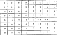
The display result of active matrix part 111 before Fig. 7 is illustrated in and proofreaies and correct.In Fig. 7, though the matrix size of active matrix part 111 is 8 * 8, it is optional.Symbol X represents non-homogeneous part (pixel).Brightness (gray shade scale) level is in 0 to 100 scope, and the brightness that show is 50 equably.
What Fig. 8 represented is resulting display message after the displaying contents that is obtained Fig. 7 by CCD gamma camera device 101 is then by A/D converter 103 digital conversion.Difference between the brightness value of the part that heterogeneity is handled and the brightness value of peripheral part is bigger.In whole display part, brightness value gradually changes from a last left side to bottom right.Yet as mentioned above, because variation is little, people's visual sense feeling does not have problem.
Fig. 9 represents is the brightness (50) that will show and the result of the difference between the display message shown in Figure 8.Obtain this result and this result is used as control information with signal processor 104.
Figure 10 is illustrated in formation (acquisition) control information afterwards by the new video signal displayed of wanting is carried out the result that digital conversion obtains.This result represents the output information of A/D converter 117.
Figure 11 is illustrated in the Correction Processor 116 result that the information addition with the information of Fig. 9 and Figure 10 is drawn.This result is the output information of Correction Processor 116.When this output information is inputed to active matrix part 111, the heterogeneity of active matrix part 111 display parts is proofreaied and correct, so that on active matrix part 111, show the information of Figure 10.
Figure 12 represents with the medial filter of signal processor 104 display message of Fig. 8 to be handled resulting result, does not carry out simple subtraction.
Figure 13 represents to deduct the resulting result of result of Figure 12 from the display message of Fig. 8.This result is a control information.Medial filter only allows the less variable quantity of vision signal (display message) by also therefore removing heterogeneity information.From the information that after removing heterogeneity information, obtains, deduct raw information, thereby can obtain heterogeneity information.
When using laplacian filter, can obtain the information of the big change point of expression.Figure 14 is illustrated in the Correction Processor 116 control information of Figure 13 and the resulting result of information addition among Figure 10.This result represents the output information of Correction Processor 116.
Figure 15 represents the display message of demonstration on the active matrix part 111.Display message comprises little variable quantity but does not comprise big variable quantity, consequently is difficult to aware the heterogeneity on the display part.
In this embodiment, use analog gray scale grade type driver, but also can use digital gray scale grade type driver.When using digital gray scale grade type driver, do not need D/A converter 120.Similarly, when flying-spot video generator 107 generation digital signals and when digital video signal is input to LCD device 110, do not need A/D converter 117 yet.
Can when forming the active matrix part, on glass substrate, be formed for driving the driving circuit of pixel TFT, perhaps can be provided with and the corresponding unijunction wafer of driving circuit from being dynamically connected by (COG) technology or magnetic with TFT, similar with patch memory 115.
[second embodiment 2]
Fig. 6 represents to have according to another embodiment of the present invention the corrective system of LCD device.Present embodiment is different with first embodiment, the display message that show obtain and correction is carried out repeatedly.
In Fig. 6, the corrective system of this embodiment is included in LCD device 620 and control information (correction data) generator 600 that forms on the glass substrate (not shown).LCD device 620 has an active matrix part 621, a gate driver 622, a Source drive 623,624, one memory devices of a Memory Controller (patch memory 625), a Correction Processor 626, an A/D converter 627,628, one clock generators 629 of a synchronous divider, and a D/A converter 630.
In control information generator 600, will input to A/D converter 627 by the vision signal of the video signal generator 607 output synchronous divider 628 by LCD device 620, so that vision signal is carried out digital conversion.The vision signal that digital conversion is crossed is input to Correction Processor 626.Since in initial step, in Correction Processor 626, do not proofread and correct, thus vision signal is input to D/A converter 630, so that vision signal is carried out analog-converted.After this, by Source drive 623 vision signal of analog-converted is inputed to active matrix part 621, so that show.Till this step, just carry out and conventional LCD device identical operations.
The formation of control information (correction data) is as follows.
CCD by control information generator 600 videotapes the light displaying contents that machine 601 obtains demonstration on the active matrix part 621 of LCD device 620.CCD gamma camera device 601 has a CCD gamma camera etc.Because from the vision signal of device 601 output generally all is a feeble signal, so it is amplified with amplifier 602.The vision signal of having amplified is carried out digital conversion and is input to signal processor 604 then by A/D converter 603.
In the first displaying contents process of acquisition, will be stored in the storer 608 by the control information that signal processor 604 obtains.Control information also is stored in the patch memory 625 by switch 612 and data write unit 605.After carrying out correction similar to Example 1, show again and then obtain second displaying contents.Will be by totalizer 610 by signal processor 604 control information (corresponding to second displaying contents) that obtains and control information (corresponding to the first displaying contents) addition that is stored in the storer 608, consequently the control information with the addition gained is stored in storer 609 and the patch memory 625.LCD device 620 is proofreaied and correct again.After this, show and then obtain the 3rd displaying contents.With totalizer 611 with the output information of signal processor 604 be stored in storer 609 in control information (corresponding to second displaying contents) mutually adduction deposit in the patch memory 625 by switch 612 and data write unit 605.
By repeating to obtain and proofread and correct displaying contents many times, can carry out more high-precision correction.In this embodiment, proofread and correct, also can carry out twice, four time or correction more frequently although carried out three times.
When driving patch memory and active matrix part, carry out 1 identical operations with embodiment.
The present invention is different from the bearing calibration that the use of routine has redundant pixel TFT. With of the present invention Bearing calibration and conventional bearing calibration are combined, can obtain further improvement effect.
As mentioned above, in the present invention, will be stored in the LCD device about defective and heteropical information In the memory of introducing in the part, with canned data to inputing to the vision signal place of LCD device Reason is proofreaied and correct the defective on the display part of LCD device and heterogeneity then, therefore, and energy Carry out high-quality demonstration.
Claims (18)
1. method of operating active matrix type display, wherein said active matrix type display comprises:
The active array type display part;
Source drive;
Be used to store the nonvolatile memory of control information; With
Correction Processor;
Described method comprises:
Incoming video signal is to described Correction Processor;
To be input to described Correction Processor from the control information of nonvolatile memory;
Proofread and correct described vision signal by described control information;
Vision signal after proofreading and correct is input to described Source drive; With
By the vision signal display image on described active array type display part after the described correction that is input to Source drive.
2. according to the method for the operation active matrix type display of claim 1, wherein said active matrix type display is a LCD.
3. according to the method for the operation active matrix type display of claim 1, wherein said active matrix type display also comprises gate driver and divider synchronously.
4. according to the method for the operation active matrix type display of claim 1, wherein said active array type display part comprises thin film transistor (TFT).
5. according to the method for the operation active matrix type display of claim 1, wherein said Source drive is included in the thin film transistor (TFT) that forms on the substrate identical with described active array type display part.
6. according to the method for the operation active matrix type display of claim 1, wherein said nonvolatile memory is a flash memories.
7. method of operating active matrix type display, wherein said active matrix type display comprises:
The active array type display part;
Source drive;
Be used to store the nonvolatile memory of control information;
Correction Processor; With
A/D converter;
Described method comprises:
Input analog video signal is to described A/D converter;
Described analog video signal is converted to digital video signal;
Digital video signal is input to described Correction Processor;
To be input to described Correction Processor from the control information of nonvolatile memory;
Proofread and correct described digital video signal by described control information;
Digital video signal after proofreading and correct is input to described Source drive; With
By the digital video signal display image on described active array type display part after the described correction that is input to Source drive.
8. according to the method for the operation active matrix type display of claim 7, wherein said active matrix type display is a LCD.
9. according to the method for the operation active matrix type display of claim 7, wherein said active matrix type display also comprises gate driver and divider synchronously.
10. according to the method for the operation active matrix type display of claim 7, wherein said active array type display part comprises thin film transistor (TFT).
11. according to the method for the operation active matrix type display of claim 7, wherein said Source drive is included in the thin film transistor (TFT) that forms on the substrate identical with described active array type display part.
12. according to the method for the operation active matrix type display of claim 7, wherein said nonvolatile memory is a flash memories.
13. a method of operating active matrix type display, wherein said active matrix type display comprises:
The active array type display part;
Source drive;
Be used to store the nonvolatile memory of control information;
Correction Processor;
A/D converter; With
D/A converter;
Described method comprises:
Input analog video signal is to described A/D converter;
Described analog video signal is converted to digital video signal;
Digital video signal is input to described Correction Processor;
To be input to described Correction Processor from the control information of nonvolatile memory;
Proofread and correct described digital video signal by described control information;
Digital video signal after proofreading and correct is input to described D/A converter;
Digital video signal after the described correction is converted to analog video signal after the correction; With
By the analog video signal display image on described active array type display part after the described correction that is input to Source drive.
14. according to the method for the operation active matrix type display of claim 13, wherein said active matrix type display is a LCD.
15. according to the method for the operation active matrix type display of claim 13, wherein said active matrix type display also comprises gate driver and divider synchronously.
16. according to the method for the operation active matrix type display of claim 13, wherein said active array type display part comprises thin film transistor (TFT).
17. according to the method for the operation active matrix type display of claim 13, wherein said Source drive is included in the thin film transistor (TFT) that forms on the substrate identical with described active array type display part.
18. according to the method for the operation active matrix type display of claim 13, wherein said nonvolatile memory is a flash memories.
Applications Claiming Priority (2)
| Application Number | Priority Date | Filing Date | Title |
|---|---|---|---|
| JP07953394A JP3672586B2 (en) | 1994-03-24 | 1994-03-24 | Correction system and operation method thereof |
| JP79533/1994 | 1994-03-24 |
Related Parent Applications (1)
| Application Number | Title | Priority Date | Filing Date |
|---|---|---|---|
| CNB2004100322069A Division CN100381921C (en) | 1994-03-24 | 1995-03-24 | Method for operating correction system |
Publications (2)
| Publication Number | Publication Date |
|---|---|
| CN1932954A CN1932954A (en) | 2007-03-21 |
| CN100520900C true CN100520900C (en) | 2009-07-29 |
Family
ID=13692637
Family Applications (4)
| Application Number | Title | Priority Date | Filing Date |
|---|---|---|---|
| CN95104532A Expired - Lifetime CN1089522C (en) | 1994-03-24 | 1995-03-24 | System for correcting display device and method for correction the same |
| CNB2004100322069A Expired - Lifetime CN100381921C (en) | 1994-03-24 | 1995-03-24 | Method for operating correction system |
| CNB2006101014098A Expired - Lifetime CN100520900C (en) | 1994-03-24 | 1995-03-24 | Method for operating active-matrix display |
| CNB011394374A Expired - Lifetime CN1149528C (en) | 1994-03-24 | 2001-11-20 | Method for operating correction system |
Family Applications Before (2)
| Application Number | Title | Priority Date | Filing Date |
|---|---|---|---|
| CN95104532A Expired - Lifetime CN1089522C (en) | 1994-03-24 | 1995-03-24 | System for correcting display device and method for correction the same |
| CNB2004100322069A Expired - Lifetime CN100381921C (en) | 1994-03-24 | 1995-03-24 | Method for operating correction system |
Family Applications After (1)
| Application Number | Title | Priority Date | Filing Date |
|---|---|---|---|
| CNB011394374A Expired - Lifetime CN1149528C (en) | 1994-03-24 | 2001-11-20 | Method for operating correction system |
Country Status (5)
| Country | Link |
|---|---|
| US (4) | US5793344A (en) |
| JP (1) | JP3672586B2 (en) |
| KR (2) | KR100272821B1 (en) |
| CN (4) | CN1089522C (en) |
| TW (1) | TW269033B (en) |
Families Citing this family (103)
| Publication number | Priority date | Publication date | Assignee | Title |
|---|---|---|---|---|
| JP3672586B2 (en) * | 1994-03-24 | 2005-07-20 | 株式会社半導体エネルギー研究所 | Correction system and operation method thereof |
| TW290678B (en) | 1994-12-22 | 1996-11-11 | Handotai Energy Kenkyusho Kk | |
| US6069600A (en) * | 1996-03-28 | 2000-05-30 | Kabushiki Kaisha Toshiba | Active matrix type liquid crystal display |
| US6697037B1 (en) * | 1996-04-29 | 2004-02-24 | International Business Machines Corporation | TFT LCD active data line repair |
| JPH09318929A (en) * | 1996-05-29 | 1997-12-12 | Toshiba Corp | Liquid crystal display device and method for correcting display unevenness |
| JP2937130B2 (en) * | 1996-08-30 | 1999-08-23 | 日本電気株式会社 | Active matrix type liquid crystal display |
| US6166782A (en) * | 1997-01-29 | 2000-12-26 | Apple Computer, Inc. | Method and apparatus for reducing visibility of damping wires in aperture grill display tubes |
| US6667494B1 (en) | 1997-08-19 | 2003-12-23 | Semiconductor Energy Laboratory Co., Ltd. | Semiconductor device and semiconductor display device |
| US6717179B1 (en) * | 1997-08-19 | 2004-04-06 | Semiconductor Energy Laboratory Co., Ltd. | Semiconductor device and semiconductor display device |
| JP3980178B2 (en) * | 1997-08-29 | 2007-09-26 | 株式会社半導体エネルギー研究所 | Nonvolatile memory and semiconductor device |
| JPH11143379A (en) * | 1997-09-03 | 1999-05-28 | Semiconductor Energy Lab Co Ltd | Semiconductor display device correcting system and its method |
| US6476779B1 (en) * | 1998-03-31 | 2002-11-05 | Sony Corporation | Video display device |
| JP3632505B2 (en) * | 1999-06-18 | 2005-03-23 | セイコーエプソン株式会社 | Image display device |
| US6909411B1 (en) * | 1999-07-23 | 2005-06-21 | Semiconductor Energy Laboratory Co., Ltd. | Display device and method for operating the same |
| US6618115B1 (en) * | 1999-11-19 | 2003-09-09 | Semiconductor Energy Laboratory Co., Ltd. | Defective pixel compensation system and display device using the system |
| JP4754682B2 (en) * | 1999-11-19 | 2011-08-24 | 株式会社半導体エネルギー研究所 | Display device |
| JP2001209358A (en) * | 2000-01-26 | 2001-08-03 | Seiko Epson Corp | Correction of irregularity in display image |
| US20020113268A1 (en) * | 2000-02-01 | 2002-08-22 | Jun Koyama | Nonvolatile memory, semiconductor device and method of manufacturing the same |
| US6414661B1 (en) | 2000-02-22 | 2002-07-02 | Sarnoff Corporation | Method and apparatus for calibrating display devices and automatically compensating for loss in their efficiency over time |
| US6577531B2 (en) * | 2000-04-27 | 2003-06-10 | Semiconductor Energy Laboratory Co., Ltd. | Nonvolatile memory and semiconductor device |
| US7088322B2 (en) * | 2000-05-12 | 2006-08-08 | Semiconductor Energy Laboratory Co., Ltd. | Semiconductor device |
| TW522374B (en) * | 2000-08-08 | 2003-03-01 | Semiconductor Energy Lab | Electro-optical device and driving method of the same |
| US6992652B2 (en) * | 2000-08-08 | 2006-01-31 | Semiconductor Energy Laboratory Co., Ltd. | Liquid crystal display device and driving method thereof |
| US7180496B2 (en) * | 2000-08-18 | 2007-02-20 | Semiconductor Energy Laboratory Co., Ltd. | Liquid crystal display device and method of driving the same |
| US6987496B2 (en) * | 2000-08-18 | 2006-01-17 | Semiconductor Energy Laboratory Co., Ltd. | Electronic device and method of driving the same |
| TW518552B (en) * | 2000-08-18 | 2003-01-21 | Semiconductor Energy Lab | Liquid crystal display device, method of driving the same, and method of driving a portable information device having the liquid crystal display device |
| TW514854B (en) * | 2000-08-23 | 2002-12-21 | Semiconductor Energy Lab | Portable information apparatus and method of driving the same |
| US7184014B2 (en) * | 2000-10-05 | 2007-02-27 | Semiconductor Energy Laboratory Co., Ltd. | Liquid crystal display device |
| US6950109B2 (en) * | 2000-10-23 | 2005-09-27 | Sun Microsystems, Inc. | Multi-spectral color correction |
| JP3899817B2 (en) * | 2000-12-28 | 2007-03-28 | セイコーエプソン株式会社 | Liquid crystal display device and electronic device |
| US6747623B2 (en) | 2001-02-09 | 2004-06-08 | Semiconductor Energy Laboratory Co., Ltd. | Liquid crystal display device and method of driving the same |
| JP3614792B2 (en) * | 2001-04-23 | 2005-01-26 | ウインテスト株式会社 | Pixel inspection apparatus and pixel inspection method for active matrix display |
| JP3606270B2 (en) * | 2001-07-09 | 2005-01-05 | セイコーエプソン株式会社 | Electro-optical device driving method, image processing circuit, electronic apparatus, and correction data generation method |
| US7088052B2 (en) * | 2001-09-07 | 2006-08-08 | Semiconductor Energy Laboratory Co., Ltd. | Light emitting device and method of driving the same |
| TWI273539B (en) | 2001-11-29 | 2007-02-11 | Semiconductor Energy Lab | Display device and display system using the same |
| JP3913534B2 (en) * | 2001-11-30 | 2007-05-09 | 株式会社半導体エネルギー研究所 | Display device and display system using the same |
| KR100462600B1 (en) * | 2002-04-02 | 2004-12-20 | 삼성전자주식회사 | Apparatus and method for controlling automatically adjustment of power supply in a plasma display panel drive system |
| US6911781B2 (en) * | 2002-04-23 | 2005-06-28 | Semiconductor Energy Laboratory Co., Ltd. | Light emitting device and production system of the same |
| KR100859514B1 (en) * | 2002-05-30 | 2008-09-22 | 삼성전자주식회사 | Liquid crystal display and driving apparatus thereof |
| JP4067878B2 (en) * | 2002-06-06 | 2008-03-26 | 株式会社半導体エネルギー研究所 | Light emitting device and electric appliance using the same |
| US6982727B2 (en) * | 2002-07-23 | 2006-01-03 | Broadcom Corporation | System and method for providing graphics using graphical engine |
| TW559756B (en) * | 2002-08-26 | 2003-11-01 | Chi Mei Optoelectronics Corp | Defective pixel remedy device and method of LCD panel |
| US6933967B2 (en) * | 2002-09-10 | 2005-08-23 | Sony Corporation | Color reference system for display monitor |
| US7298355B2 (en) * | 2002-12-27 | 2007-11-20 | Semiconductor Energy Laboratory Co., Ltd. | Display device |
| US20040246280A1 (en) * | 2003-06-06 | 2004-12-09 | Credelle Thomas Lloyd | Image degradation correction in novel liquid crystal displays |
| GB2410143A (en) * | 2004-01-13 | 2005-07-20 | Hassan Paddy Abdel Salam | Display calibration cradle for portable device |
| KR20050109223A (en) * | 2004-05-14 | 2005-11-17 | 삼성전자주식회사 | Apparatus and method for generating reference data for image signal modification |
| JP4549762B2 (en) * | 2004-07-13 | 2010-09-22 | シャープ株式会社 | Image signal processing apparatus and method |
| US20060044299A1 (en) * | 2004-08-31 | 2006-03-02 | Jian Wang | System and method for compensating for a fabrication artifact in an electronic device |
| DE602004024895D1 (en) | 2004-10-25 | 2010-02-11 | Barco Nv | Optical correction for light panels with high uniformity |
| US7639849B2 (en) | 2005-05-17 | 2009-12-29 | Barco N.V. | Methods, apparatus, and devices for noise reduction |
| JP2006345436A (en) * | 2005-06-10 | 2006-12-21 | Fuji Xerox Co Ltd | Image processor and image processing system |
| JP2007025635A (en) * | 2005-06-17 | 2007-02-01 | Fujitsu Hitachi Plasma Display Ltd | Plasma display device and method of treating the same |
| TWI424408B (en) * | 2005-08-12 | 2014-01-21 | Semiconductor Energy Lab | Semiconductor device, display device and electronic device equipped with the semiconductor device |
| GB2431276B (en) * | 2005-10-14 | 2008-11-12 | Cambridge Display Tech Ltd | Display monitoring systems |
| KR101136286B1 (en) * | 2005-10-17 | 2012-04-19 | 엘지디스플레이 주식회사 | Flat Display Apparatus And Picture Quality Controling Method Thereof |
| KR101127843B1 (en) | 2005-10-25 | 2012-03-21 | 엘지디스플레이 주식회사 | Flat Display Apparatus And Picture Quality Controling Method Thereof |
| KR101137856B1 (en) | 2005-10-25 | 2012-04-20 | 엘지디스플레이 주식회사 | Flat Display Apparatus And Picture Quality Controling Method Thereof |
| KR101201314B1 (en) * | 2005-11-16 | 2012-11-14 | 엘지디스플레이 주식회사 | Method of Fabricating Flat Display Panel |
| TWI273312B (en) * | 2005-11-30 | 2007-02-11 | Au Optronics Corp | Display device and panel module |
| US7911498B2 (en) | 2005-12-12 | 2011-03-22 | Novatek Microelectronics Corp. | Compensation device for non-uniform regions in flat panel display and method thereof |
| US20070132790A1 (en) * | 2005-12-14 | 2007-06-14 | Syntax Brillian Corp. | Method and apparatus for calibrating a color display panel and related manufacturing and service method |
| KR100769193B1 (en) * | 2006-02-06 | 2007-10-23 | 엘지.필립스 엘시디 주식회사 | Flat Display Apparatus, Picture Quality Controling Method And Apparatus Thereof |
| TW200732739A (en) * | 2006-02-21 | 2007-09-01 | Chi Mei Optoelectronics Corp | Liquid crystal display utilizing redundancy line as repair line and method of repairing the same |
| JP2007264088A (en) * | 2006-03-27 | 2007-10-11 | Funai Electric Co Ltd | Display device, image persistence correction system, and image persistence correction method |
| US7460133B2 (en) * | 2006-04-04 | 2008-12-02 | Sharp Laboratories Of America, Inc. | Optimal hiding for defective subpixels |
| US7596024B2 (en) * | 2006-07-14 | 2009-09-29 | Semiconductor Energy Laboratory Co., Ltd. | Nonvolatile memory |
| KR100866368B1 (en) * | 2006-08-29 | 2008-11-03 | 노바텍 마이크로일렉트로닉스 코포레이션 | Compensation hardware device for non-uniform regions in flat panel display |
| US20080117231A1 (en) * | 2006-11-19 | 2008-05-22 | Tom Kimpe | Display assemblies and computer programs and methods for defect compensation |
| CN101192362B (en) * | 2006-12-01 | 2010-09-22 | 康佳集团股份有限公司 | LEDLED display screen on site single-point calibration device and its method |
| KR101332134B1 (en) | 2006-12-29 | 2013-11-21 | 엘지디스플레이 주식회사 | Liquid crystal display device |
| TWI375198B (en) * | 2007-05-17 | 2012-10-21 | Tpo Displays Corp | A system for displaying images |
| CN101315745B (en) * | 2007-05-28 | 2012-11-28 | 统宝光电股份有限公司 | Image display system and its moire defect elimination method |
| US10810918B2 (en) * | 2007-06-14 | 2020-10-20 | Lg Display Co., Ltd. | Video display device capable of compensating for display defects |
| EP2048642A1 (en) | 2007-10-10 | 2009-04-15 | Barco NV | Reducing visibility of display errors |
| JP4681033B2 (en) * | 2008-07-31 | 2011-05-11 | 株式会社イクス | Image correction data generation system, image data generation method, and image correction circuit |
| JP5362753B2 (en) * | 2008-07-31 | 2013-12-11 | 株式会社イクス | Image quality adjustment apparatus and image correction data generation program |
| CN101377450B (en) * | 2008-09-19 | 2012-10-03 | 李鑫 | System and method for extracting lightness data of display screen dot matrix |
| CN101377918B (en) * | 2008-09-19 | 2013-02-27 | 李鑫 | Electronic display screen system, method and system for correcting electronic display screen brightness |
| WO2010146733A1 (en) * | 2009-06-18 | 2010-12-23 | シャープ株式会社 | Defect inspection method and defect inspection device for display panel |
| WO2012005284A1 (en) * | 2010-07-07 | 2012-01-12 | シャープ株式会社 | Liquid-crystal display device |
| KR101830679B1 (en) * | 2010-07-29 | 2018-02-22 | 삼성디스플레이 주식회사 | Apparatus for testing a display panel and method thereof |
| CN101916539B (en) * | 2010-08-20 | 2012-10-03 | 西安诺瓦电子科技有限公司 | System and method for correcting brightness and chromaticity of LED display screen point by point |
| JP4777472B1 (en) * | 2010-08-24 | 2011-09-21 | 株式会社イクス | Image correction data generation system, display correction data generation method, and image correction data generation program for display panel using non-polished glass |
| US9183811B2 (en) | 2011-04-01 | 2015-11-10 | Sharp Kabushiki Kaisha | Method of correcting unevenness of display panel and correction system |
| WO2013157627A1 (en) * | 2012-04-20 | 2013-10-24 | 株式会社ニコン | Electronic apparatus and correction method |
| CN103559863B (en) * | 2013-11-11 | 2015-06-17 | 西安诺瓦电子科技有限公司 | LED lamp panel and LED display screen |
| WO2015092952A1 (en) * | 2013-12-20 | 2015-06-25 | パナソニックIpマネジメント株式会社 | Display unevenness correction device, display device, display unevenness correction method, and method for manufacturing display device |
| CN105096815A (en) * | 2014-05-06 | 2015-11-25 | 西安诺瓦电子科技有限公司 | Method for correcting brightness and chrominance of LED display screen, and LED display screen system |
| WO2016083928A1 (en) | 2014-11-28 | 2016-06-02 | Semiconductor Energy Laboratory Co., Ltd. | Image processing device, display system, and electronic device |
| KR102287907B1 (en) * | 2015-06-22 | 2021-08-10 | 삼성디스플레이 주식회사 | Degradation compensator of organic light emitting diode display device |
| US10152812B2 (en) * | 2015-10-23 | 2018-12-11 | Sharp Kabushiki Kaisha | Odd-even veil view for FFS |
| US20190130811A1 (en) * | 2016-04-13 | 2019-05-02 | Sakai Display Products Corporation | Correction data generation device, computer program, and method for generating correction data |
| US20200043443A1 (en) * | 2016-10-26 | 2020-02-06 | Sakai Display Products Corporation | Correction system |
| WO2018116381A1 (en) * | 2016-12-20 | 2018-06-28 | 堺ディスプレイプロダクト株式会社 | Control circuit, display device, correction system, control method and correction method |
| US10909895B2 (en) * | 2016-12-20 | 2021-02-02 | Sakai Display Products Corporation | Correction system, display panel, display device, correction method, and storage medium |
| CN107179123B (en) * | 2017-04-21 | 2019-01-29 | 华南理工大学 | The brightness calibration and measurement method that camera is merged with LED light |
| CN108831374B (en) * | 2018-06-22 | 2020-06-30 | 京东方科技集团股份有限公司 | Pixel luminance compensation method and device |
| JP2020086419A (en) * | 2018-11-28 | 2020-06-04 | 雄二 橋本 | Adjustment method and adjustment system for obtaining uniformity of plural control objects and conveyer device and adjusted equipment |
| US11210772B2 (en) * | 2019-01-11 | 2021-12-28 | Universal City Studios Llc | Wearable visualization device systems and methods |
| US11030944B1 (en) * | 2019-12-04 | 2021-06-08 | Capital One Services, Llc | Systems and methods for correcting ambient-light illuminance differences of ambient light directed onto regions of a display |
| US11776503B2 (en) * | 2020-05-28 | 2023-10-03 | Apple Inc. | Generating display data based on modified ambient light luminance values |
| US11763758B2 (en) | 2021-05-27 | 2023-09-19 | Sharp Kabushiki Kaisha | Luminance unevenness correction system and luminance unevenness correction method |
Family Cites Families (43)
| Publication number | Priority date | Publication date | Assignee | Title |
|---|---|---|---|---|
| US4224615A (en) * | 1978-09-14 | 1980-09-23 | Texas Instruments Incorporated | Method of using a liquid crystal display device as a data input device |
| JPS61137194A (en) | 1984-12-10 | 1986-06-24 | キヤノン株式会社 | Correction/driving of liquid crystal display panel |
| JPS61243495A (en) | 1985-04-20 | 1986-10-29 | 三洋電機株式会社 | Compensation of uneven display for liquid crystal display unit |
| JPH0766251B2 (en) | 1985-05-10 | 1995-07-19 | ソニー株式会社 | Liquid crystal display |
| JPS6337785A (en) | 1986-07-31 | 1988-02-18 | Toshiba Electric Equip Corp | Video display device |
| JPS63148781A (en) | 1986-12-12 | 1988-06-21 | Nec Corp | Liquid crystal display device |
| JPS63199323A (en) | 1987-02-16 | 1988-08-17 | Matsushita Electric Ind Co Ltd | Video signal correcting circuit |
| JP2653099B2 (en) * | 1988-05-17 | 1997-09-10 | セイコーエプソン株式会社 | Active matrix panel, projection display and viewfinder |
| JPH02131287A (en) | 1988-11-11 | 1990-05-21 | Nec Corp | Display device |
| JPH0311390A (en) * | 1989-06-08 | 1991-01-18 | Matsushita Electric Ind Co Ltd | Projection type picture display device |
| DE69022891T2 (en) * | 1989-06-15 | 1996-05-15 | Matsushita Electric Ind Co Ltd | Device for compensating video signals. |
| IL91303A0 (en) | 1989-08-14 | 1990-03-19 | Ibm Israel | System for displaying images on a cathode ray tube |
| JPH03164793A (en) | 1989-11-24 | 1991-07-16 | Sharp Corp | Liquid crystal display device |
| JP2566044B2 (en) | 1990-05-25 | 1996-12-25 | 日産自動車株式会社 | Heater unit structure of vehicle air conditioner |
| JPH04142591A (en) | 1990-10-04 | 1992-05-15 | Seiko Epson Corp | Liquid crystal display device |
| JPH04165395A (en) | 1990-10-29 | 1992-06-11 | Nec Corp | Correcting method of distortion in image magnification |
| JPH04184485A (en) | 1990-11-20 | 1992-07-01 | Seiko Epson Corp | Driving circuit for liquid crystal display device |
| JPH04233514A (en) * | 1990-12-28 | 1992-08-21 | Sharp Corp | Active matrix substrate |
| JP3033912B2 (en) | 1990-12-28 | 2000-04-17 | 日本電気ホームエレクトロニクス株式会社 | Video signal correction circuit for liquid crystal display |
| US5751261A (en) * | 1990-12-31 | 1998-05-12 | Kopin Corporation | Control system for display panels |
| US5150238A (en) * | 1991-03-04 | 1992-09-22 | Nview Corporation | Active matrix lcd projection system with anti-reflective characteristics |
| JP3123095B2 (en) * | 1991-03-29 | 2001-01-09 | 株式会社日立製作所 | Screen defect detection method for display |
| KR970001735B1 (en) * | 1991-04-05 | 1997-02-14 | Sharp Kk | A liquid crystal display device and a liquid crystal display system using the liquid crystal display device |
| JPH0511725A (en) | 1991-07-04 | 1993-01-22 | Fujitsu Ltd | Gradation control deivce for display |
| JPH0667620A (en) * | 1991-07-27 | 1994-03-11 | Semiconductor Energy Lab Co Ltd | Image display device |
| US5245326A (en) * | 1991-08-19 | 1993-09-14 | International Business Machines Corp. | Calibration apparatus for brightness controls of digitally operated liquid crystal display system |
| JP3116457B2 (en) * | 1991-09-13 | 2000-12-11 | 株式会社村田製作所 | Convergence measurement device |
| JPH0583659A (en) | 1991-09-24 | 1993-04-02 | Toshiba Corp | Automatic adjusting device for electronic circuit |
| US5216504A (en) * | 1991-09-25 | 1993-06-01 | Display Laboratories, Inc. | Automatic precision video monitor alignment system |
| JPH05154728A (en) | 1991-12-06 | 1993-06-22 | Hitachi Ltd | Product with memory device and mixed-flow manufacturing device thereof |
| JPH05169356A (en) | 1991-12-17 | 1993-07-09 | Hitachi Ltd | Adjustment and inspection method to each subject in production line and location mounting base plate thereof |
| JPH0618839A (en) | 1992-06-29 | 1994-01-28 | Victor Co Of Japan Ltd | Liquid crystal projector device |
| JPH0624182A (en) * | 1992-07-07 | 1994-02-01 | Japan Servo Co Ltd | Greeting card |
| JPH06138849A (en) * | 1992-10-30 | 1994-05-20 | Sharp Corp | Liquid crystal video display device |
| US5608422A (en) * | 1992-11-27 | 1997-03-04 | Sanyo Electric Co., Ltd. | Automatic contrast adjusting device |
| US5477359A (en) * | 1993-01-21 | 1995-12-19 | Sharp Kabushiki Kaisha | Liquid crystal projector having a vertical orientating polyimide film |
| JP2988815B2 (en) | 1993-11-12 | 1999-12-13 | シャープ株式会社 | Liquid crystal drive |
| CA2138363C (en) * | 1993-12-22 | 1999-06-22 | Yasuyuki Todokoro | Electron beam generating apparatus, image display apparatus, and method of driving the apparatuses |
| JP3672586B2 (en) | 1994-03-24 | 2005-07-20 | 株式会社半導体エネルギー研究所 | Correction system and operation method thereof |
| KR970010101B1 (en) * | 1994-06-30 | 1997-06-21 | Daewoo Electronics Co Ltd | Post-processing method of digital transmission pictures |
| US5874988A (en) * | 1996-07-08 | 1999-02-23 | Da Vinci Systems, Inc. | System and methods for automated color correction |
| JP2001075542A (en) | 2000-07-10 | 2001-03-23 | Semiconductor Energy Lab Co Ltd | Correction system and its operating method |
| JP2001075523A (en) | 2000-07-10 | 2001-03-23 | Semiconductor Energy Lab Co Ltd | Correction system and its operating method |
-
1994
- 1994-03-24 JP JP07953394A patent/JP3672586B2/en not_active Expired - Fee Related
-
1995
- 1995-03-21 US US08/407,685 patent/US5793344A/en not_active Expired - Lifetime
- 1995-03-22 TW TW084102783A patent/TW269033B/zh not_active IP Right Cessation
- 1995-03-24 CN CN95104532A patent/CN1089522C/en not_active Expired - Lifetime
- 1995-03-24 CN CNB2004100322069A patent/CN100381921C/en not_active Expired - Lifetime
- 1995-03-24 CN CNB2006101014098A patent/CN100520900C/en not_active Expired - Lifetime
- 1995-03-24 KR KR1019950006290A patent/KR100272821B1/en not_active IP Right Cessation
-
1998
- 1998-06-26 US US09/104,978 patent/US6549183B1/en not_active Expired - Fee Related
-
2000
- 2000-06-09 KR KR1020000031595A patent/KR100305276B1/en not_active IP Right Cessation
-
2001
- 2001-11-20 CN CNB011394374A patent/CN1149528C/en not_active Expired - Lifetime
-
2003
- 2003-04-04 US US10/406,318 patent/US6987497B2/en not_active Expired - Fee Related
-
2006
- 2006-01-03 US US11/322,342 patent/US20060109231A1/en not_active Abandoned
Also Published As
| Publication number | Publication date |
|---|---|
| KR100272821B1 (en) | 2000-11-15 |
| US6549183B1 (en) | 2003-04-15 |
| CN100381921C (en) | 2008-04-16 |
| TW269033B (en) | 1996-01-21 |
| CN1538374A (en) | 2004-10-20 |
| JP3672586B2 (en) | 2005-07-20 |
| CN1149528C (en) | 2004-05-12 |
| US20060109231A1 (en) | 2006-05-25 |
| US6987497B2 (en) | 2006-01-17 |
| KR950034027A (en) | 1995-12-26 |
| KR100305276B1 (en) | 2001-11-07 |
| US20030193489A1 (en) | 2003-10-16 |
| CN1352447A (en) | 2002-06-05 |
| US5793344A (en) | 1998-08-11 |
| CN1089522C (en) | 2002-08-21 |
| CN1126919A (en) | 1996-07-17 |
| JPH07261719A (en) | 1995-10-13 |
| CN1932954A (en) | 2007-03-21 |
Similar Documents
| Publication | Publication Date | Title |
|---|---|---|
| CN100520900C (en) | Method for operating active-matrix display | |
| CN102231016B (en) | Method, device and system for compensating brightness of liquid crystal module | |
| CN100510907C (en) | Liquid crystal display and driving method thereof | |
| US6429841B1 (en) | Active matrix liquid crystal display apparatus and method for flicker compensation | |
| US5235448A (en) | Liquid crystal display having proportional tft channel width | |
| CN101246675A (en) | Driving method and driving apparatus of liquid crystal display | |
| US7978163B2 (en) | Apparatus and method for driving a liquid crystal display | |
| CN107481686B (en) | Method for improving display state of liquid crystal panel, liquid crystal panel and liquid crystal display | |
| US8085278B2 (en) | Method for setting compensation region for irregular defect region in manage display device | |
| KR20080042446A (en) | Liquid crystal display device and manufacturing method thereof | |
| US11320923B2 (en) | Control circuit for a display apparatus | |
| CN1975850B (en) | Method and apparatus for driving data in liquid crystal display screen | |
| CN100594412C (en) | Liquid crystal display apparatus and drive method thereof | |
| CN101490737B (en) | Liquid crystal driving circuit, driving method, and liquid crystal display apparatus | |
| US6392631B1 (en) | Process for displaying data on a matrix display | |
| US20120038597A1 (en) | Pre-programming of in-pixel non-volatile memory | |
| KR20070093540A (en) | Display device | |
| CN112447134A (en) | Gray scale correction method and system for display panel | |
| TW559756B (en) | Defective pixel remedy device and method of LCD panel | |
| JP2001075523A (en) | Correction system and its operating method | |
| CN201203738Y (en) | Liquid crystal display device | |
| CN101371290A (en) | Liquid crystal panel driver, liquid crystal panel driving method, liquid crystal display | |
| US20080062210A1 (en) | Driving device, display apparatus having the same and method of driving the display apparatus | |
| US6518947B1 (en) | LCD column driving apparatus and method | |
| CN110111753A (en) | The driving method and device of display panel |
Legal Events
| Date | Code | Title | Description |
|---|---|---|---|
| C06 | Publication | ||
| PB01 | Publication | ||
| C10 | Entry into substantive examination | ||
| SE01 | Entry into force of request for substantive examination | ||
| C14 | Grant of patent or utility model | ||
| GR01 | Patent grant | ||
| C17 | Cessation of patent right | ||
| CX01 | Expiry of patent term |
Expiration termination date: 20150324 Granted publication date: 20090729 |