Summary of the invention
The present invention puts in view of the above-mentioned problems and makes, its purpose, and being to provide can slimming, water proofing property or dust tightness is good and resistance to impact etc. is good, and visual good electro-optical device and protection member, and manufacture method.
And purpose of the present invention has adopted so electronic equipment of electro-optical device for providing.
In order to address the above problem, electro-optical device of the present invention, possess: the electrooptic panel that between a pair of substrate, has electrooptic layer, protection member that at least one side for aforesaid base plate installs, be made of the light-transmitting substrate that the aforementioned electric optic panel is protected and the retaining member that the aforementioned electric optic panel is kept; It is characterized in that: at aforementioned protection member, the thick part of the thickness of aforementioned light-transmitting substrate is set and is arranged at the thin part of the outer rim of aforementioned light-transmitting substrate, between thick part of the thickness of aforementioned light-transmitting substrate and thin part, have stage portion; Aforementioned retaining member has the junction surface that the aforementioned stage portion corresponding to aforementioned protection member engages; Aforementioned light-transmitting substrate and aforementioned electric optic panel are fitted by adhesive linkage.
According to electro-optical device so; can make it to possess resistance to impact, water proofing property, dust tightness for the electrooptic panel in this electro-optical device by the protection member; and because be provided with stage portion at the light-transmitting substrate that constitutes the protection member; so can make retaining member be engaged in (being embedded in) this stage portion, make the electrooptic panel and the retaining member of band protection member integrated.Under this situation,,, can help the slimming of this electro-optical device so can prevent to follow in maximization to the device of the installation of retaining member because needn't prepare to be used for electrooptic panel is installed to the special member of retaining member in addition.And,,, become very good from the visuality of the demonstration of electrooptic panel so between this protection member and electrooptic panel, can not form air layer because protection member and electrooptic panel are bonded.
And in order to address the above problem, electro-optical device of the present invention is characterized in that: the aforementioned light-transmitting substrate of aforementioned protection member and aforementioned electric optic panel, fitted by gel-type resin.
According to electro-optical device so, can directly fit aforementioned protection member and aforementioned electric optic panel.By protection member and electrooptic panel are fitted, between protection member and electrooptic panel, can not form air layer, become very good from the visuality of the demonstration of electrooptic panel.And,, then be difficult to produce the substrate uneven homogenize of (cell gap) at interval of electrooptic panel if applying is undertaken by gel-type resin.
And, in order to address the above problem, electro-optical device of the present invention is characterized in that: the junction surface of aforementioned retaining member, between the aforementioned thin part of aforementioned electric optic panel and aforementioned light-transmitting substrate, be held, and be engaged in the stage portion of aforementioned light-transmitting substrate and be embedded into; The aforementioned electric optic panel is adhesively fixed by adhesive linkage at the interarea of the side with aforementioned stage portion of aforementioned light-transmitting substrate.
And, in above-mentioned, it is characterized in that: between the aforementioned junction surface of aforementioned retaining member and aforementioned electric optic panel, adhesive linkage is set also, fixes the aforementioned junction surface and the aforementioned electric optic panel of aforementioned retaining member.By so constituting, also can realize integrated with the electrooptic panel of protection member and retaining member suitably, its bed knife becomes more reliable.
And, in order to address the above problem, electro-optical device of the present invention, it is characterized in that: the aforementioned thin part of aforementioned light-transmitting substrate, between the junction surface of aforementioned electric optic panel and aforementioned retaining member, be held, and the aforementioned stage portion of aforementioned light-transmitting substrate is engaged in the junction surface of aforementioned retaining member and is embedded into; The aforementioned electric optic panel is adhesively fixed by adhesive linkage at the interarea with the side opposition side with aforementioned stage portion of aforementioned light-transmitting substrate.By so being adhesively fixed, can realize integrated with protection electrooptic panel of member and retaining member suitably, its bed knife becomes more reliable.
And; in order to address the above problem; electro-optical device of the present invention; it is characterized in that: aforementioned protection member; the 2nd light-transmitting substrate that overlapping the 1st light-transmitting substrate and major-surface-area are littler than the 1st light-transmitting substrate constitutes; the part of stretching from the outer rim of aforementioned the 2nd light-transmitting substrate at aforementioned the 1st light-transmitting substrate forms aforementioned thin part; and form aforementioned stage portion between the outer rim of aforementioned part of stretching and aforementioned the 2nd light-transmitting substrate, the junction surface of aforementioned retaining member is configured corresponding to this stage portion.
According to electro-optical device so, can make it to possess resistance to impact, water proofing property, dust tightness for the electrooptic panel in this electro-optical device by the protection member.And; so protect member to constitute because make by the 1st light-transmitting substrate and the 2nd light-transmitting substrate; and the 2nd less comparatively speaking light-transmitting substrate of major-surface-area (area of plate face) is set in the plane domain that is included in the 1st light-transmitting substrate; outer rim at this protection member forms aforementioned thin part; and between the part of stretching (aforementioned thin part) of the outer rim of the 2nd light-transmitting substrate and the 1st light-transmitting substrate, form aforementioned stage portion; so can make the end (junction surface) of retaining member be engaged in the stage portion of this protection member, can make the electrooptic panel and the retaining member of band protection member integrated.Under this situation,,, can help the slimming of this electro-optical device so can prevent to follow in maximization to the device of the installation of retaining member because needn't prepare to be used for electrooptic panel is installed to the special member of retaining member in addition.
And; in order to address the above problem; electro-optical device of the present invention; it is characterized in that: aforementioned retaining member is the housing that places the aforementioned electric optic panel; this housing is provided with the peristome corresponding to the viewing area of aforementioned electric optic panel; the end of the aforementioned peristome of aforementioned retaining member is aforementioned junction surface; the part that the thickness of the aforementioned light-transmitting substrate of aforementioned protection member is thick is embedded into corresponding to the aforementioned peristome of aforementioned retaining member, and the aforementioned stage portion of aforementioned protection member is engaged in the aforementioned junction surface of aforementioned retaining member.By so constituting, can realize integrated with the electrooptic panel of protection member and retaining member suitably.
In electro-optical device of the present invention; can: aforementioned retaining member is formed with the cylindrical body of hollow form; inside in this cylindrical body keeps the aforementioned electric optic panel; on the other hand; form the junction surface of retaining member in the inboard of this cylindrical body; the junction surface of this retaining member is meshed with the stage portion of aforementioned protection member.According to so constituting, can realize integrated with the electrooptic panel of protection member and retaining member suitably.Also have, the junction surface of retaining member for example can constitute as the jut of the inboard that protrudes in cylindrical body, and this jut can be meshed with the stage portion of aforementioned protection member.
And in electro-optical device of the present invention, the aforementioned electric optic panel can be suspended state (only by being supported with being adhesively fixed of the light-transmitting substrate that is disposed at upside and fixing state) in the hollow form inside of aforementioned retaining member.By so making electrooptic panel is suspended state, and vibration resistance is improved.Also have, the so-called suspended state under this situation is meant that electrooptic panel is not supported from its vertical direction downside.
And in order to address the above problem, electro-optical device of the present invention is characterized in that: make adhesive linkage between the aforementioned thin part of the aforementioned junction surface of aforementioned retaining member and aforementioned protection member, fixing aforementioned protection member and aforementioned retaining member.
And in order to address the above problem, electro-optical device of the present invention is characterized in that: fit aforementioned the 1st light-transmitting substrate and aforementioned the 2nd light-transmitting substrate, and aforementioned the 1st light-transmitting substrate fits in the aforementioned electric optic panel; Aforementioned the 2nd light-transmitting substrate is disposed at and aforementioned electric optic panel opposition side with respect to aforementioned the 1st light-transmitting substrate.
Aforementioned protection member; can be following structure: have the 1st light-transmitting substrate that fits in the aforementioned electric optic panel; with the 2nd light-transmitting substrate that fits in the 1st light-transmitting substrate; outer rim at aforementioned the 1st light-transmitting substrate has aforementioned stage portion and forms aforementioned thin part; aforementioned the 2nd light-transmitting substrate; be disposed at and aforementioned electric optic panel opposition side with respect to aforementioned the 1st light-transmitting substrate; and the junction surface of aforementioned retaining member (end of aforementioned peristome) is by the aforementioned stage portion and aforementioned the 2nd light-transmitting substrate clamping of aforementioned the 1st light-transmitting substrate.By so constituting, can realize suitably that also its bed knife becomes more reliable with protecting the integrated of member electrooptic panel and retaining member.
And in order to address the above problem, electro-optical device of the present invention is characterized in that: fit aforementioned the 1st light-transmitting substrate and aforementioned the 2nd light-transmitting substrate, and aforementioned the 2nd light-transmitting substrate fits in the aforementioned electric optic panel; Aforementioned the 1st light-transmitting substrate is disposed at and aforementioned electric optic panel opposition side with respect to aforementioned the 2nd light-transmitting substrate.
And; in electro-optical device of the present invention; can for: make adhesive linkage between the aforementioned thin part of the protection member that the junction surface (end of aforementioned peristome) and aforementioned the 1st light-transmitting substrate of aforementioned retaining member are stretched from the outer rim of aforementioned the 2nd light-transmitting substrate of aforementioned protection member; fixing aforementioned protection member and aforementioned housing, the aforementioned electric optic panel is adhesively fixed by adhesive linkage and aforementioned protection member on the surface of the upside of this electrooptic panel.
By so electrooptic panel being adhesively fixed, can realize integrated with protection electrooptic panel of member and retaining member suitably.And then; stretch thin part from the outer rim of aforementioned the 2nd light-transmitting substrate by the 1st light-transmitting substrate aforementioned protection member, aforementioned with stage portion; with the aforementioned electric optic panel; the junction surface of the aforementioned retaining member of clamping (end of aforementioned peristome); between aforementioned the 2nd light-transmitting substrate and aforementioned electric optic panel, and insert and put adhesive linkage between the end of the aforementioned peristome of aforementioned retaining member and the aforementioned electric optic panel and fix.By so constituting, also can realize integrated with the electrooptic panel of protection member and retaining member suitably.
And in order to address the above problem, electro-optical device of the present invention is characterized in that: among aforementioned the 1st light-transmitting substrate and aforementioned the 2nd light-transmitting substrate, the substrate that is equipped on aforementioned electric optic panel side is made of tempered glass.By so adopting the substrate of tempered glass, the transmitance of protection member is improved, the degree of freedom of designability uprises, and can help the raising of the visuality of electrooptic panel.
And in order to address the above problem, electro-optical device of the present invention is characterized in that: among aforementioned the 1st light-transmitting substrate and aforementioned the 2nd light-transmitting substrate, the substrate that is equipped on a side of aforementioned electric optic panel side opposition side is made of resin.By so making the substrate that is disposed at aforementioned electric optic panel side opposition side (display surface side) is resin substrate, can prevent the breakage of this protection member etc. than glass substrate.
And in order to address the above problem, electro-optical device of the present invention is characterized in that: at least one side of aforementioned the 1st light-transmitting substrate and aforementioned the 2nd light-transmitting substrate is to make light after being polarized incide the polarization plates of aforementioned electric optic panel.Make the inscape of polarization plates if so as the protection member, then needn't be to the subsidiary polarization plates of electrooptic panel, and be resin system by for example making polarization plates, can prevent the breakage of this protection member etc. than glass substrate.
And in order to address the above problem, electro-optical device of the present invention is characterized in that: zone at the aforementioned junction surface of the aforementioned retaining member of the aforementioned thin part that embeds aforementioned light-transmitting substrate sets the shading member that has comprised predetermined pattern that should the zone.According to so constituting, can produce light-proofness or ornamental (decoration that is undertaken by the shading graph of being scheduled to) in the presumptive area of this electro-optical device by the shading member.Especially if the shading member carries out shading to the non-display part of electrooptic panel, the visuality that then also helps to show improves.
Especially, can for: see that with the plane shape that covers aforementioned stage portion forms aforementioned shading member, aim at aforementioned electric optic panel and aforementioned light-transmitting substrate on the other hand, make aforementioned shading member plane see the non-display part that is positioned at electrooptic panel.If so the stage portion of light-transmitting substrate is carried out shading, and the non-display part of electrooptic panel is carried out shading, then the visuality of Xian Shiing is improved.
And; at least one side at aforementioned the 1st light-transmitting substrate and aforementioned the 2nd light-transmitting substrate; set under the situation of shading member of predetermined pattern; can for: see that with the plane shape that covers aforementioned stage portion forms aforementioned shading member; aim at aforementioned electric optic panel and aforementioned protection member on the other hand, make that aforementioned shading member planarity ground is overlapping and be positioned at the non-display part of electrooptic panel.If so the thin part of protection member is carried out shading, and the non-display part of electrooptic panel is carried out shading, then the visuality of Xian Shiing is improved.
Also have, said in the present invention shading member except the light (demonstration) from electrooptic panel is fully carried out the shading, also comprises the half light-proofness member that a part is carried out shading.And, except the shading member of black, also comprised the painted member that is colored as predetermined colour (for example red, blue, green etc.).
And in order to address the above problem, electronic equipment of the present invention is characterized in that: possess and be recorded in above-mentioned electro-optical device in any.So band is protected the electro-optical device of member, for example can constitute the display part of electronic equipment.And, possessing the electronic equipment of this electro-optical device, the resistance to impact height is suitable as the information communication device of portable usefulness such as portable telephone, pager, PDA, notebook-sized personal computer.Moreover, in electronic equipment of the present invention,, formation is simplified more if the housing of this electronic equipment is kept electrooptic panel as retaining member.
And; in order to address the above problem; protection member of the present invention constitutes by the light-transmitting substrate that the surface of electrooptic panel is protected, and it is characterized in that: the outer rim setting of this light-transmitting substrate have stage portion, optionally make the thickness attenuation part.
According to so protecting member, can protect electrooptic panel from avoiding aspects such as impact, and because constitute, so this stage portion can be fixed at housing etc. by the translucent glass substrate that has stage portion in outer rim.Thereby; to be fixed in the electrooptic panel of this protection member in housing etc.; can improve water proofing property, dust tightness for electrooptic panel; and because needn't prepare in addition to be used for will band protection member electrooptic panel be installed to the special member of housing etc.; so can prevent to follow in maximization, can help the slimming of device as a whole to the device of the installation of housing etc.And this protection member is because be made of glass substrate, so light transmission is good, and the degree of freedom of designability uprises, and can help the visuality of electrooptic panel to improve.
And in order to address the above problem, protection member of the present invention is characterized in that: at aforementioned light-transmitting substrate, form the shading member that the presumptive area of aforementioned electric optic panel is carried out shading.By so formation of shading member, the visuality of electrooptic panel is improved more.And, if make aforementioned shading member, form with the shape of the aforementioned stage portion of the overlapping covering in ground of planarity at least, then can be suitably the housing that is fixed in stage portion etc. be carried out shading, and then the visuality of electrooptic panel is improved more.
And; in order to address the above problem; the manufacture method of protection member of the present invention; it is manufacture method by the protection member that light-transmitting substrate constituted that the surface of electrooptic panel is protected; it is characterized in that: comprise that stage portion forms operation; this stage portion forms operation, by implementing mask etching for light-transmitting substrate, form in the outer rim of this light-transmitting substrate have stage portion, make the thickness attenuation part.
According to manufacture method so, can make above-mentioned protection member of the present invention suitably.Especially, in the present invention, because constitute the protection member, so the etching by utilizing mask to carry out can be easily forms stage portion in the outer rim of this glass substrate by the glass substrate of light transmission.
And, in order to address the above problem, the manufacture method of protection member of the present invention, it is manufacture method by the protection member that light-transmitting substrate constituted that the surface of electrooptic panel is protected, it is characterized in that, comprising: stage portion forms operation, and this stage portion forms operation, implement mask etching for the large-scale light transmission mother metal that can make a plurality of these protection members, form in position corresponding to the outer rim of each protection member that will form have stage portion, make the thickness attenuation part; With cut off operation, this cuts off operation, aforementioned make the thickness attenuation part cut off aforementioned light transmission mother metal (partly) by the outer rim configuration thin thickness of each protection member of disjunction, be divided into each and protect member.
According to manufacture method so, can make above-mentioned protection member of the present invention suitably.Especially, in the present invention, making the light-transmitting substrate of protection member is glass substrate, by the etch processes of implementing to be undertaken by mask, can be easily forms stage portion in the outer rim of this glass substrate.And; because as above-mentionedly to large-scale light transmission mother metal employing base glass material, each forms the thin part with stage portion in the lump to each protection member by mask etching, becomes high in the extreme so make efficient; its result can provide cheap protection member.
Also have, in above-mentioned manufacture method, after aforementioned stage portion forms operation, can comprise that the shading member of the shading member that forms predetermined pattern forms operation.And, in the manufacture method that has adopted large-scale light transmission mother metal, can comprise that after aforementioned cut-out operation the shading member of the shading member that forms predetermined pattern forms operation.And then the method as forming the shading member for example can adopt print process, and the position as forming the shading member can be the substrate inboard of stage portion, to cover the shape of stage portion at least, is formed at and this stage portion plane read fortune position overlapped.And then, also can implement the operation that substrate is ground or carry out chemical enhanced operation and handle as finishing.
Embodiment
Below, about suitable embodiment of the present invention,, and then describe particularly with reference to accompanying drawing.Also have, in each figure,, make engineer's scale different because of each layer, each member in order to make each layer, each member size on accompanying drawing for the degree that can discern.
The 1st embodiment
Fig. 1, be model utility be expressed as the stereographic map that the integral body of portable telephone 10 of an embodiment of electronic equipment of the present invention constitutes; Fig. 2 is that the sectional view that near the section of display part of portable telephone 10 constitutes is represented on model utility ground; Fig. 3 is that model utility ground expression possesses the sectional view that constitutes in the section of the display device (electro-optical device) of this portable telephone 10.
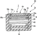
As be shown among Fig. 1 ground, and the portable telephone 10 of present embodiment, the display part 1, operating portion (operation push-button) 2, the antenna 3 that possess plastic housing 14, expose from this housing 14 constitute.Display part 1, the section that has as being shown among Fig. 2 constitutes, and is exposed to outside display device (electro-optical device) 1a and the backlight 40 that is assembled in the housing 14 is constituted as main body with display window (peristome) 14e (with reference to Fig. 1) from housing 14.Also have, backlight 40 is held in housing 14 by predetermined circuit substrate 44.
Display device 1a is made of liquid-crystal apparatus in the present embodiment, has: liquid crystal panel (electrooptic panel) 28, and protect member 19 and will protect member 19 to be installed to the adhesive linkage 22 of liquid crystal panel 28.At this, display device 1a is fixed in the inboard of the housing (retaining member) 14 of the portable telephone 10 that tubular ground constituted, and is to sandwich the structure of the end of this housing 14 between protection member 19 and adhesive linkage 22, integrated with this housing 14.
Liquid crystal panel 28, as be shown among Fig. 3 ground, and comprise 2 transparent substrates 30,30, be attached at the polarization plates 31,31 of substrate 30,30 separately, to around the encapsulant 32 that seals and enclose 34 formations of liquid crystal (electrooptic layer) by their formed spaces.2 plate bases 30 form respectively with any of glass or plastics.
Also have, liquid crystal panel 28, if with type of drive, can adopt at simple matrix liquid crystal display panel, the static drive display panels of panel self, or adopt with three terminal on-off elements of TFT (thin film transistor (TFT)) representative or with the active matrix liquid crystal display panel of the two-terminal on-off element of MIM (metal-insulator-metal type) representative without on-off element; If with electro-optical characteristic, can adopt TN type, STN type, guest-host type, inversion of phases, strong dielectric type etc., various types of liquid crystal panels.
On the other hand; be installed on the protection member 19 of liquid crystal panel 28 by adhesive linkage 22, by being formed with acryl resin, abundant visible light transmissive; and for example have that the light-transmitting substrate 18 of the thickness of 1mm~2mm degree constitutes, the intensity of drop impact when having ability and carrying etc.And, light-transmitting substrate 18, the state that has had stage portion (slot part) D with the outer rim that cuts the one interarea forms the part 18a of thin thickness, with the state of the thick part of thickness with adhesive linkage 22 (being liquid crystal panel 28) subtend, fit this light-transmitting substrate 18 and liquid crystal panel 28.Thereby the part that stretches out in the outside of light-transmitting substrate 18 than unfertile land is used as the part 18a of thin thickness.Promptly, light-transmitting substrate 18 becomes and has the thicker part of thickness comparatively speaking that is arranged at the substrate center side, part 18a with the thin thickness comparatively speaking of the outer edge side that is arranged at this light-transmitting substrate 18, and between the part of thicker part of thickness and thin thickness, be provided with the formation of stage portion D, embed end (junction surface) 14a of housing 14 at this stage portion D.
And, follow in setting of stage portion D so, at the applying interface of light-transmitting substrate 18 and adhesive linkage 22 (being liquid crystal panel 28), be formed on the space that this stage portion D is opened on the outside, embed the part of the housing 14 of portable telephone 10 in this space.At this, end (junction surface) 14a that is equipped on the peristome of housing 14 is embedded in aforesaid space, and housing 14 and display device 1a are by integrated.Also have, the end 14a of the peristome of housing, the jut that highlights as the main part 14b from the housing 14 of tubular constitutes.
On the other hand, the degree of depth of stage portion D (and the height between the bonding plane of liquid crystal panel 28 and the thick stage portion 18a surface that approaches of substrate), corresponding to the size of the end 14a of peristome and design, be designed to the identical degree of depth of thickness with the end 14a of peristome at this.Its result, the surface of the inner face (faces of adhesive linkage 22 sides of the thick part of light-transmitting substrate) of the inner face of the end 14a of the peristome of housing (retaining member) 14 (with the thin opposite face of a side that part disposed of light-transmitting substrate) and light-transmitting substrate 18 is as one man smooth, becomes the formation that is contacted with adhesive linkage 22 respectively.Also have, light-transmitting substrate 18 can also pass through urethane resin, epoxy resin except acryl resin, and perhaps glass substrate etc. constitutes.
Liquid crystal panel 28 and protection member 19 are carried out bonding adhesive linkage 22; transparent elastic resin for the scope of the whole display surface that is formed at liquid crystal panel 28; Thermocurable with silicones, acryl resin, urethane resin etc. of silica gel etc. for example; and after heat curing, can also keep elasticity; be the material of abundant visible light transmissive, about 30 μ m are formed with thickness.
Constitute the transparent elastic resin of adhesive linkage 22, have cementability, can be attached at polarization plates 31, and the light-transmitting substrate 18 of protection member 19 of liquid crystal panel 28 by its bonding force.And the transparent elastic resin is being favourable without bonding agent, the point that just can be adhered to liquid crystal panel 28 and light-transmitting substrate 18 securely by heat curing.Moreover the transparent elastic resin also keeps predetermined elasticity after this heat curing.So, the transparent elastic resin, because have cementability, so without bonding agent etc., just can keep the state that protection member 19 and liquid crystal panel 28 are closely bonded.
According to portable telephone 10 as above-mentioned present embodiment; because constitute the display device 1a of display part 1; constituted by liquid-crystal apparatus with the surface of protection member 19 covering liquid crystal panel 28; so resistance to impact is good, be difficult to produce the unfavorable condition of liquid crystal panel 28 impact damage when falling etc. etc.And, except resistance to impact, can also make liquid crystal panel 28 have water proofing property or dust tightness.
And then; because be provided with stage portion D at the light-transmitting substrate 18 that constitutes protection member 19; so, protecting the space that forms between member 19 (light-transmitting substrate 18) and the adhesive linkage 22 corresponding to the thin part 18a of light-transmitting substrate 18 at the applying interface by protection member 19 and liquid crystal panel 28 are fitted by adhesive linkage 22.Then, by at end (junction surface) 14a of formed space embedding, can make the liquid crystal panel 28 and the housing 14 of band protection member integrated as the peristome of the housing 14 of retaining member.Under this situation,,, can help the slimming of this liquid-crystal apparatus 1a so can prevent to follow in maximization to the device of the installation of housing 14 because needn't prepare to be used for housing 14 is installed to the special member of liquid crystal panel 28 in addition.And,,, become high in the extreme from the visuality of the demonstration of liquid crystal panel 28 so between this protection member 19 and liquid crystal panel 28, can not form air layer because protection member 19 and liquid crystal panel 28 are directly fitted.
And, in the present embodiment, cylindrical body with hollow form forms housing 14, inside in this cylindrical body keeps liquid crystal panel 28, on the other hand, be formed at the end 14a of peristome of overshooting shape of the inboard of this cylindrical body, the state with the stage portion D that is embedded in light-transmitting substrate 18 is sandwiched between thin the part 18a and adhesive linkage 22 of light-transmitting substrate 18.By so constituting, can realize integrated with the liquid crystal panel 28 of protection member and housing 14 suitably, because housing 14 becomes the shape that covers with protection member 19, so that the intensity of display device 1a becomes is high in the extreme.
Also have, in the present embodiment, protection member 19 and liquid crystal panel 28 are aligned, and make that the thin part 18a of light-transmitting substrate 18 is overlapping with the outer shroud of liquid crystal panel 28, and promptly the part 18a and the encapsulant 32 that approach of light-transmitting substrate 18 are overlapping.Aim at, particularly, as be shown among Figure 21 ground, undertaken by alignment mark 41 that forms in the position that is overlapped in thin part 18a of protection member 19 and the alignment mark 42 that forms in the position that is overlapped in encapsulant 32 of liquid crystal panel 28 are coincided.Also have, behind aligning, have the circuit substrate 12 of the external connection terminals of liquid crystal panel 28, becoming is exposed to the outside from protection member 19.
The 2nd embodiment
Below, describe about the 2nd embodiment of the display device of the display part 1 that constitutes portable telephone 10.
Fig. 4 is the figure that the section of the display device 1b of model utility ground expression the 2nd embodiment constitutes, and is the accompanying drawing corresponding to Fig. 2 of the display device 1a of the 1st embodiment.At this; about display device 1b; the engagement of the formation of protection member 19 and housing 14 and these protection members 19 and housing 14; inequality with the display device 1a of Fig. 2 and Fig. 3; about adhesive linkage 22 and liquid crystal panel 28; so, only describe about protection member 19 and housing 14 because be that the formation identical with the display device 1a of Fig. 2 and Fig. 3 omitted explanation.
In the present embodiment, also the light-transmitting substrate 18 at retaining member 19 forms stage portion D and thin part 18a, and the thick part of protection member 19 fits to liquid crystal panel 28 by adhesive linkage 22.And, also form the stage portion that is engaged in the light-transmitting substrate 18 of retaining member 19 corresponding to stage portion D at housing 14, these stage portion 18a and stage portion (junction surface) 14a subtend and meshing.Thereby in the 2nd embodiment, the junction surface 14a of housing (retaining member) 14 is used as stage portion, and is not the formation that protrudes in the inboard that places liquid crystal panel 28 for the junction surface of housing (retaining member) 14.
And, and then, in the present embodiment, form shading member 17 at protection member 19.It is patterned that this shading member 17 sees that with the plane thin part 18a with stage portion D and light-transmitting substrate 18 carries out overlapping shape, and then carry out overlapping form with the encapsulant 32 (with reference to Fig. 3) with liquid crystal panel 28 and be aligned.
Aim at; particularly; as being shown among Figure 21 ground, alignment mark 41 that the position by the thin part 18a that is overlapped in stage portion D and light-transmitting substrate 18 that makes at protection member 19 forms and the alignment mark 42 that forms in the position that is overlapped in encapsulant 32 of liquid crystal panel 28 coincide and carry out.Also have, as among Figure 21 also shown in, shading member 17 planes see that the thin part 18a with stage portion D and light-transmitting substrate 18 carries out overlapping formation, this shading member 17 is aligned to the viewing area of encirclement liquid crystal panel 28.
By the display device 1b of the 2nd above embodiment, also can by protection member 19 for the liquid crystal panel 28 in this display device 1b make it to possess resistance to impact, water proofing property, dust tightness.And because protection member 19 so to constitute light transmission by light-transmitting substrate 18 good, and the degree of freedom of designability uprises, and can help the visuality of liquid crystal panel 28 to improve.And then, because the shape with the viewing area that surrounds liquid crystal panel 28 forms shading member 17, so can produce light-proofness or ornamental (decoration that is undertaken by predetermined shading graph) in the presumptive area of display device by shading member 17, and the visuality of demonstration is improved.
Also have, shading member 17 except the light (demonstration) from liquid crystal panel 28 is fully carried out the shading, also comprises the half light-proofness member that a part is carried out shading.Perhaps, except the shading member of black, can also comprise the painted member that is colored as predetermined colour (for example red, blue, green etc.).Also have, constitute by crome metal, in addition, also can adopt the metal material that carbon, titanium is scattered in resin black in the photoresists, nickel etc. though shading member 17 adopts.Perhaps, as low reflection usefulness, can also adopt 2 layers of structure of crome metal and chromium oxide.
The 3rd embodiment
Below, describe about the 3rd embodiment of the display device of the display part 1 that constitutes portable telephone 10.Fig. 5 is, the figure that the section of the display device 1c of model utility ground expression the 3rd embodiment constitutes is the accompanying drawing corresponding to Fig. 2 of the display device 1a of the 1st embodiment.
In the present embodiment, also the light-transmitting substrate 18 at retaining member 19 forms stage portion D and thin part 18a, and protection member 19 fits in liquid crystal panel 28.And, at housing 14, formation is from outstanding jut (junction surface) 14a of its inner face, between the thin part 18a of light-transmitting substrate 18 and adhesive linkage 22 clamping under the state of jut (junction surface) 14a, jut (junction surface) 14a embeds the stage portion D of light-transmitting substrate 18.In the present embodiment, by so embedding, can realize the integrated of housing 14 and the liquid crystal panel 28 of being with the protection member.
And then in the present embodiment, display surface side (promptly different with adhesive linkage 22 face sides) the configuration polarization plates 31 at protection member 19 places in the opening of housing 14.This polarization plates 31 is used to make rectilinearly polarized light to incide liquid crystal panel 28, does not form polarization plates in the display surface side (being adhesive linkage 22 sides) of liquid crystal panel 28 in the present embodiment.
By the display device 1c of the 3rd above embodiment, also can by protection member 19 for the liquid crystal panel 28 in this display device 1c make it to possess resistance to impact, water proofing property, dust tightness.And because protection member 19 so to constitute light transmission by light-transmitting substrate 18 good, and the degree of freedom of designability uprises, and can help the visuality of liquid crystal panel 28 to improve.And then, in the present embodiment, because polarization plates 31 is formed at the outside of protecting member 19, so can produce the effect that prevents that glass from splashing.
The 4th embodiment
Fig. 6 is that the sectional view that near the section of display part of portable telephone 10 constitutes is represented on model utility ground; Fig. 7, be model utility be illustrated in the sectional view that the section of the display device (electro-optical device) that is possessed in this portable telephone 10 constitutes.
Display device 1a is made of liquid-crystal apparatus in the present embodiment, has: liquid crystal panel (electrooptic panel) 28, and protect member 19 and will protect member 19 to be installed on the adhesive linkage 22 of liquid crystal panel 28.At this, display device 1a is fixed in the inboard of the housing (retaining member) 14 of the portable telephone 10 that tubular ground constitutes, and is integrated with this housing 14.
Liquid crystal panel 28, as be shown among Fig. 7 ground, and comprise 2 transparent substrates 30,30, be attached at the polarization plates 31,31 of substrate 30,30 separately, to around the encapsulant 32 that seals and enclosing in 34 formations of liquid crystal (electrooptic layer) by their formed spaces.2 plate bases 30 are with any institute formation respectively of glass or plastics.
And, be installed on the protection member 19 of liquid crystal panel 28 by adhesive linkage 22, formed abundant visible light transmissive, and have the thickness of 1mm~2mm degree for example and constitute, the intensity of the drop impact when having ability and carrying etc. with the glass substrate of light transmission.And, light-transmitting substrate 18, outer rim by etching excision one interarea has stage portion (slot part) D and thin part 18a, with with the face of the thin part 18a that has formed this stage portion D and the light-transmitting substrate 18 not face of homonymy and the state of adhesive linkage 22 (being liquid crystal panel 28) subtend, fit this light-transmitting substrate 18 and liquid crystal panel 28.
And,, also form junction surface 14a at the housing 14 of portable telephone 10 corresponding to the thin part 18a of so stage portion D and light-transmitting substrate 18.At this junction surface 14a, as constituting from the outstanding jut 14a of the main part 14b of the housing 14 of tubular.Then, this jut 14a is engaged in the stage portion D of light-transmitting substrate 18, and housing 14 and display device 1a are by integrated.Also have; housing 14; cylindrical body with hollow form is formed; be held with suspended state (only with the face of the thin part 18a of stage portion D that has formed protection member 19 and light-transmitting substrate 18 state that is adhesively fixed of the face of homonymy not) at the inside of this cylindrical body liquid crystal panel 28; from outstanding jut (junction surface) 14a of the inner face of this cylindrical body, be meshed with the stage portion D of light-transmitting substrate 18.
The degree of depth of stage portion D designs corresponding to the size of jut (junction surface) 14a, is designed to the degree of depth identical with the thickness of jut 14a at this.Particularly, the thickness of jut 14a is 0.2mm~0.8mm (for example 0.4mm), and the degree of depth of stage portion D is to be constituted with the identical size of thickness of this jut 14a.Its result, the surface of the surface of jut 14a (with the thin part 18a of light-transmitting substrate 18 surface of a side of subtend not) and light-transmitting substrate 18 (with the surface of the thick part of the light-transmitting substrate 18 of configuration liquid crystal panel 28 side opposition sides) consistently become smooth (becoming a plane) makes the aesthetic feeling raising of portable telephone 10.At light-transmitting substrate 18, also can be provided with stage portion D, thin part 18a, and the non-display area of the liquid crystal panel 28 shading member that carries out shading.
Liquid crystal panel 28 and protection member 19 are carried out bonding adhesive linkage 22; transparent elastic resin for the scope of the whole display surface that is formed at liquid crystal panel 28; Thermocurable with silicones, acryl resin, urethane resin etc. of silica gel etc. for example; and after heat curing, can also keep elasticity; be the material of abundant visible light transmissive, about 30 μ m are formed with thickness.
Constitute the transparent elastic resin of adhesive linkage 22, have cementability, can be attached at polarization plates 31, and the light-transmitting substrate 18 of protection member 19 of liquid crystal panel 28 by its bonding force.And the transparent elastic resin is being favourable without bonding agent, the point that just can be adhered to liquid crystal panel 28 and light-transmitting substrate 18 securely by heat curing.Moreover the transparent elastic resin also keeps predetermined elasticity after this heat curing.So, the transparent elastic resin, because have cementability, so without bonding agent etc., just can keep the state that protection member 19 and liquid crystal panel 28 are closely bonded.
According to portable telephone 10 as above-mentioned present embodiment; because constitute the display device 1a of display part 1; constituted by liquid-crystal apparatus with the surface of protection member 19 covering liquid crystal panel 28; so resistance to impact is good, be difficult to produce the unfavorable condition of liquid crystal panel 28 impact damage when falling etc. etc.And, except resistance to impact, can also make liquid crystal panel 28 have water proofing property or dust tightness.And because protection member 19 is made of light-transmitting substrate 18, so light transmission is good, and the degree of freedom of designability uprises, and can help the visuality of liquid crystal panel 28 to improve.
Also have, in the present embodiment, protection member 19 and liquid crystal panel 28 are aligned, and make that the thin part 18a of light-transmitting substrate 18 is overlapping with the outer shroud of liquid crystal panel 28, and promptly the part 18a and the encapsulant 32 that approach of light-transmitting substrate 18 are overlapping.Aim at; particularly; as being shown among Figure 21 ground, alignment mark 41 that the position by the thin part 18a that is overlapped in light-transmitting substrate 18 that makes at protection member 19 forms and the alignment mark 42 that forms in the position that is overlapped in encapsulant 32 of liquid crystal panel 28 coincide and carry out.Also have, behind aligning, have the circuit substrate 12 of the external connection terminals of liquid crystal panel 28, becoming is exposed to the outside from protection member 19.
The 5th embodiment
Below, describe about the 5th embodiment of the display device of the display part 1 that constitutes portable telephone 10.
Fig. 8 is the figure that the section of the display device 1b of model utility ground expression the 5th embodiment constitutes, and is the accompanying drawing corresponding to Fig. 2 of the display device 1a of the 1st embodiment.At this; about display device 1b, the formation of the formation of protection member 19 and the display device 1a of Fig. 3 is inequality, about adhesive linkage 22 and liquid crystal panel 28; so, only describe about protection member 19 because be that the formation identical with the display device 1a of Fig. 3 omitted explanation.
In display device 1b, the protection member 19 that liquid crystal panel 28 is protected comprises: film (the 2nd light-transmitting substrate) 18d of the 1st light-transmitting substrate 18c of the thickness 0.2mm~0.8mm degree that is made of acryl resin and thickness 0.1mm~0.25mm degree of being made of polyethylene terephthalate.That is, protection member 19 constitutes by the 1st light-transmitting substrate 18c and the 2nd light-transmitting substrate 18d, and the junction surface 14a that becomes retaining member 14 is sandwiched in the structure of the 1st light-transmitting substrate 18c and the 2nd light-transmitting substrate 18d.Also has protection member 19 under this situation, the intensity of the drop impact when also having ability and carrying etc.
Among the protection member 19, the 1st light-transmitting substrate 18c fits at face and liquid crystal panel 28 with the side opposition side with stage portion D and thin part 18a by adhesive linkage 22, and is equipped on the inside of housing 14.And, the interarea that stage portion D reaches the side of thin part 18a that has at the 1st light-transmitting substrate 18c, make that the surface (with the thin part 18a of the 1st light-transmitting substrate 18c surface of a side of subtend not) of end (junction surface) 14a of the surface of thick part of the 1st light-transmitting substrate and the peristome of housing 14 is consistent and become smooth (becoming a plane), design the thickness of end (junction surface) 14a of the peristome of the thickness of the 1st light-transmitting substrate 18c and housing 14.Particularly, the 1st light-transmitting substrate 18c has stage portion D, make the thickness of end (junction surface) 14a of the degree of depth of this stage portion D and above-mentioned peristome become in the same manner, design the end 14a of the 1st light-transmitting substrate 18c and peristome respectively, by embedded the structure of the end 14a of peristome for stage portion D, assemble the 1st light-transmitting substrate 18c and housing 14 and install.
On the other hand, the 2nd light-transmitting substrate 18d is attached on the end 14a of the 1st light-transmitting substrate 18c that becomes above-mentioned smooth (becoming a plane) and peristome.As above-mentioned ground, have stage portion D and thin part 18a at the 1st light-transmitting substrate 18c, under the state of this stage portion D and part 18a that approaches and the 2nd light-transmitting substrate 18d subtend, these the 1st light-transmitting substrate 18c and the 2nd light-transmitting substrate 18d fit.And; become: in the space that the stage portion D that passes through thin part 18a owing to the applying of these the 1st light-transmitting substrate 18c and the 2nd light-transmitting substrate 18d produces; embedded the structure of end (junction surface) 14a of aforementioned peristome, made the liquid crystal panel 28 of band protection member and housing 14 by integrated.
Also have, at binding face side (inner face side) the formation shading member 17 of the 2nd light-transmitting substrate 18d.This shading member 17 carries out shading to end (junction surface) 14a of the peristome of housing 14, the encapsulant 32 of liquid crystal panel 28 at least.Promptly, setting shading member 17 than the end 14a of these peristomes and the position of encapsulant 32 past inboard (viewing area sides), and then aligning comprises the 2nd light-transmitting substrate 18d and the housing 14 and the liquid crystal panel 28 of shading member 17, it is overlapping to make the plane see that end 14a with peristome carries out, and the plane sees that the encapsulant 32 with liquid crystal panel 28 carries out overlapping.
By the display device 1b of the 5th above embodiment, also can by protection member 19 for the liquid crystal panel 28 in this display device 1b make it to possess resistance to impact, water proofing property, dust tightness.
And because constitute protection member 19 by the 1st light-transmitting substrate 18c and the 2nd light-transmitting substrate 18d; and stage portion D and thin part 18a are set at the 1st light-transmitting substrate 18c; so by each light-transmitting substrate 18c, 18d being fitted with making this stage portion D and part 18a that approaches and the 2nd light-transmitting substrate 18d subtend; can between the 1st light-transmitting substrate 18c and the 2nd light-transmitting substrate 18d, form the space at this stage portion D and thin part 18a; the end 14a of the peristome of housing 14 is embedded, make the liquid crystal panel 28 and the housing 14 of band protection member integrated.
Under this situation,,, can help the slimming of this display device 1b so can prevent to follow in the maximization of liquid crystal panel 28 to the device of the installation of housing 14 because needn't prepare to be used for housing 14 is installed on the special member of liquid crystal panel 28 in addition.And; because the 1st light-transmitting substrate 18c and the liquid crystal panel 28 of protection member 19 are fitted by adhesive linkage 22; so between this protection member 19 and liquid crystal panel 28, can not form air layer, become high in the extreme from the visuality of the demonstration of liquid crystal panel 28.
Also have, under this situation, also form the thin part 18a of the 1st light-transmitting substrate 18c along the outer rim of the interarea of the 1st light-transmitting substrate 18c.If fit with the state of the 2nd light-transmitting substrate 18d subtend, then by the formation of thin part 18a stage portion D is produced, the formation space at the applying interface with stage portion D so and thin part 18a.Then, embed the end 14a of the peristome of housing 14 for this space.
In addition, shading member 17 except the light (demonstration) from liquid crystal panel 28 is fully carried out the shading, also comprises the half light-proofness member that a part is carried out shading.Perhaps, except the shading member of black, can also comprise the painted member that is colored as predetermined colour (for example red, blue, green etc.).Also have, constitute by crome metal, in addition, also can adopt the metal material that carbon, titanium is scattered in the resin black, nickel etc. of photoresists though shading member 17 adopts.Perhaps, as low reflection usefulness, can also adopt 2 layers of structure of crome metal and chromium oxide.And the 1st light-transmitting substrate 18c also can pass through formations such as urethane resin, epoxy resin except acryl resin.
The 6th embodiment
Secondly, describe with reference to Fig. 9 and Figure 10 about manufacture method at the protection member of from above-mentioned the 1st embodiment to the 5 embodiments, being put down in writing 19.
At first, prepare as being shown in the large-scale substrate mother metal 190 among Fig. 9 (a) and Figure 11.Large-scale substrate mother metal 190 is used for forming in the lump protection member 19, is made of glass substrate, can obtain several~tens a protection member 19 from a substrate mother metal 190.
For ready substrate mother metal 190, shelter (masking) (Figure 10: S1).At this, form stage portion is formed the position as the resist 90 of peristome.Resist 90 is formed by photoresist, and is made through exposure process.
Secondly, with the resist 90 that formed as mask, for substrate mother metal 190 carry out wet etching (Figure 10: S2), through resist peel off, matting (Figure 10: S3), form as be shown in the stage portion 18a among Fig. 9 (b).
After the part 18a that has formed stage portion D and approached, form as be shown in the shading member 17 among Fig. 9 (c).(Figure 10: S4), figure forms the shading member 17 that is made of crome metal and makes it the plane and see thin part 18a overlaid with substrate mother metal 190 to adopt print process at this.Form by serigraphy specifically, can form shading member 17 very easily according to this method.
Then; as be shown in Fig. 9 (c) middlely; carry out cut-out operation (Figure 10: S5) of substrate mother metal 190 as line L1 (with reference to Figure 11) with the central portion of the thin part 18a of substrate mother metal 190; and then as aftertreatment; (Figure 10: S6), the outer rim of finishing as being shown among Fig. 9 (d) at translucent glass substrate 18 has had the thin part 18a of this substrate and the protection member 19 of shading member 17 to carry out surface grinding, surface Hardening Treatment.Also have, as be shown among Figure 12 ground, also can carry out cut-out operation (S4) and postprocessing working procedures (S5) afterwards, form the printing process (S6) of shading member 17 for each substrate.
In addition, though in above-mentioned example by having adopted a plurality of manufacturing efficient that improve of cutting of large-scale substrate mother metal 190, can certainly make protection member 19 by each ground of a substrate as for example being shown among Figure 13.Under this situation, can omit the cut-out operation.
According to as above manufacture method, can make the protection member 19 that display device 1a, 1b possessed of present embodiment suitably.Especially, in above-mentioned manufacture method, because constitute protection member 19, so the etching by utilizing mask to carry out can form stage portion D and thin part 18a easily in the outer rim of this glass substrate by the glass substrate of light transmission.
The 7th embodiment
Figure 14 is that the sectional view that near the section of display part of portable telephone 10 constitutes is represented on model utility ground; Figure 15, be model utility be illustrated in the sectional view that the section of the display device (electro-optical device) that is possessed in this portable telephone 10 constitutes.Also have, about omitting, and describe following about the additional same-sign of identical inscape with the explanation that above-mentioned the 1st embodiment repeats mutually.Display device 1a is made of liquid-crystal apparatus in the present embodiment, has: liquid crystal panel (electrooptic panel) 28, and protect member 19 and will protect member 19 to be installed on the adhesive linkage 22 of liquid crystal panel 28.At this, display device 1a is fixed in the inboard of the housing (retaining member) 14 of the portable telephone 10 that constitutes tubular, be meshed by making the stage portion D, the 14a that are formed at protection member 19 and housing 14 respectively, and integrated with this housing 14.
On the other hand; be installed on the protection member 19 of liquid crystal panel 28 by adhesive linkage 22; constituted the 1st light-transmitting substrate 18c that this laminated body is overlapping is made of tempered glass and the 2nd light-transmitting substrate 18d that constitutes by PMMA (polymethylmethacrylate) or glass by laminated body.At this, these the 1st light-transmitting substrate 18c and the 2nd light-transmitting substrate 18d fit by curable resin mutually, and the area of the interarea of the 2nd light-transmitting substrate 18d (substrate area) constitutes than the area (substrate area) of the interarea of the 1st light-transmitting substrate 18c littlely.
And the 2nd light-transmitting substrate 18d is equipped on the plane of the 1st light-transmitting substrate 18c and sees the inboard, and its result protects the outer rim of member 19 to form the thin part 18a and the stage portion D of protection member 19 at this.Also have, the 1st light-transmitting substrate 18c thickness is 0.2mm~0.8mm (for example 0.4mm), and the thickness of the 2nd light-transmitting substrate 18d is 0.2mm~0.8mm (for example 0.4mm).By protection member 19 that applying constituted of the 1st light-transmitting substrate 18c and the 2nd light-transmitting substrate 18d so, has the intensity of the drop impact etc. of this portable telephone 10 of ability.
And, in formed stage portion D of outer rim and the thin part 18a along protection member 19, the part of the housing 14 of engagement portable telephone 10.At this; be equipped on housing 14 by the thin part 18a of the end 14a of the retaining member of opening for aforementioned protection member 19; dispose under the state that overlaps mutually of step surface; the stage portion D of splice protection member 19 and the end of retaining member (junction surface) 14a, housing 14 and protection member 19 (being liquid crystal panel 28) are by integrated thus.
By the end of the retaining member of opening (junction surface) 14a, the jut that the end surface ground that covers picture as the main part 14b from the housing 14 of tubular protrudes in the inboard constitutes.Promptly, housing 14 is constituted with the cylindrical body of hollow form, place liquid crystal panel 28 in the inside of this cylindrical body, on the other hand, embed the end 14a of the retaining member of the inboard be opened on this cylindrical body at stage portion D, and (for example making not shown adhesive linkage between the 1st light-transmitting substrate 18c with between by the end 14a of the retaining member of opening) is bonding mutually.Thereby, because liquid crystal panel 28 as between itself and the 1st light-transmitting substrate 18c, fix with its upper surface by adhesive linkage 22 followingly, so as a result of, liquid crystal panel 28 is a suspended state in the hollow form inside of housing 14, and in the vertical direction does not have the support from downside.
On the other hand, the height of stage portion D (height between the surface of the surface of the 2nd light-transmitting substrate 18d and the extension of the 1st light-transmitting substrate 18c), corresponding to being designed by the thickness of the end 14a of the retaining member of opening, the height of stage portion D is to constitute with this identical size of thickness by the end 14a of the retaining member of opening.Its result, the surface of the surface of the end 14a of retaining member (with the 1st light-transmitting substrate 18c surface of subtend not) and the 2nd light-transmitting substrate 18d (with the 1st light-transmitting substrate 18c surface of subtend not) is roughly consistent and become smooth (becoming a plane), constitutes the top layer face of portable telephone 10 respectively.Also have, the 2nd light-transmitting substrate 18d also can pass through formations such as urethane resin, epoxy resin except acryl resin.
Liquid crystal panel 28 and protection member 19 (the 1st light-transmitting substrate 18c) are carried out bonding adhesive linkage 22; transparent elastic resin for the scope of the whole display surface that is formed at liquid crystal panel 28; Thermocurable with silicones, acryl resin, urethane resin etc. of silica gel etc. for example; and after heat curing, can also keep elasticity; be the material of abundant visible light transmissive, about 30 μ m are formed with thickness.
Constitute the transparent elastic resin of adhesive linkage 22, have cementability, can be attached at polarization plates 31, and the 1st light-transmitting substrate 18c of protection member 19 of liquid crystal panel 28 by its bonding force.And the transparent elastic resin is being favourable without bonding agent, the point that just can be adhered to liquid crystal panel 28 and the 1st light-transmitting substrate 18c securely by heat curing.Also have, the transparent elastic resin also keeps predetermined elasticity after this heat curing.So, the transparent elastic resin, because have cementability, so without bonding agent etc., just can keep the state that protection member 19 and liquid crystal panel 28 are closely bonded.
According to portable telephone 10 as above-mentioned present embodiment; because constitute the display device 1a of display part 1; constituted by liquid-crystal apparatus with the surface of protection member 19 covering liquid crystal panel 28; so resistance to impact is good, be difficult to produce the unfavorable condition of liquid crystal panel 28 impact damage when falling etc. etc.And, except resistance to impact, can also make liquid crystal panel 28 have water proofing property or dust tightness.
And then, by stage portion D and thin part 18a being set, be engaged in this stage portion D by making end (junction surface) 14a as the housing 14 of retaining member at protection member 19, can make the liquid crystal panel 28 and the housing 14 of band protection member integrated.Under this situation,,, can help the slimming of this liquid-crystal apparatus 1a so can prevent to follow in maximization to the device of the installation of housing 14 because needn't prepare to be used for housing 14 is installed to the special member of liquid crystal panel 28 in addition.
And,,, become high in the extreme from the visuality of the demonstration of liquid crystal panel 28 so between this protection member 19 and liquid crystal panel 28, can not form air layer because protection member 19 and liquid crystal panel 28 are fitted by adhesive linkage 22.
And, in the present embodiment, the cylindrical body formation housing 14 with hollow form keeps liquid crystal panel 28 in the inside of this cylindrical body, on the other hand, be formed at end (junction surface) 14a of overshooting shape of inboard of this cylindrical body by with stage portion D engagement and by integrated.By so constituting, can realize integrated with the liquid crystal panel 28 of protection member and housing 14 suitably.And in the present embodiment, liquid crystal panel 28 is a suspended state in the hollow form inside of housing 14, and in the vertical direction does not have the support from downside.By so making liquid crystal panel 28 be suspended state, vibration resistance is improved.
Also have; in the present embodiment; protection member 19 and liquid crystal panel 28; be aligned; make that thin part (stretching out in the part of the 1st light-transmitting substrate 18c in the outside of the 2nd light-transmitting substrate 18d) 18a of protection member 19 is overlapping with the outer shroud of liquid crystal panel 28, promptly protect the part that approaches (stretching out in the part of the 1st light-transmitting substrate 18c in the outside of the 2nd light-transmitting substrate 18d) 18a and the encapsulant 32 of member 19 overlapping.Aim at; particularly; as be shown among Figure 21 ground, by being coincided, alignment mark 41 that forms in the position that is overlapped in stage portion D and thin part 18a of protection member 19 and the alignment mark 42 that forms in the position that is overlapped in encapsulant 32 of liquid crystal panel 28 undertaken.Also have, behind aligning, have the circuit substrate 12 of the external connection terminals of liquid crystal panel 28, becoming is exposed to the outside from protection member 19.
The 8th embodiment
Below, describe about the 8th embodiment of the display device of the display part 1 that constitutes portable telephone 10.
Figure 16 is the figure that the section of the display device 1b of model utility ground expression the 2nd embodiment constitutes, and is the accompanying drawing corresponding to Fig. 2 of the display device 1a of the 1st embodiment.At this; about display device 1b, the formation of the formation of protection member 19 and the display device 1a of Figure 15 is inequality, about adhesive linkage 22 and liquid crystal panel 28; so, only describe about protection member 19 because be that the formation identical with the display device 1a of Figure 15 omitted explanation.
In display device 1b, the protection member 19 that liquid crystal panel 28 is protected comprises: the outside substrate 18f of the inboard substrate 18e of the thickness 0.2mm~0.8mm degree that is made of tempered glass and thickness 0.2mm~0.8mm degree of being made of PMMA or glass.Also has protection member 19 under this situation, the intensity of the drop impact when also having ability and carrying etc.
Among the protection member 19, inboard substrate (the 2nd light-transmitting substrate) 18e fits in liquid crystal panel 28 by adhesive linkage 22, and face and outside substrate (the 1st light-transmitting substrate) 18f at its opposition side fits on the other hand.And in the present embodiment, inboard substrate (the 2nd light-transmitting substrate) 18e forms forr a short time than outside substrate (the 1st light-transmitting substrate) 18f major-surface-area, and inboard (by wrapping in the planarity ground) is seen on the plane that inboard substrate 18e is equipped on outside substrate 18f.Its result, the part of outside substrate (the 1st light-transmitting substrate) 18f outside the outer rim of this protection member 19 stretches out in from inboard substrate (the 2nd light-transmitting substrate) 18e forms the thin part 18a of protection member 19.
On the other hand, end (junction surface) 14a of overshooting shape is set, meshes this end 14a, the liquid crystal panel 28 of integrated these housings 14 and band protection member for the stage portion D of protection member 19 at the housing 14 that is used as retaining member.Thereby; be arranged at end (junction surface) 14a of the overshooting shape of housing 14, part (the thin part of protection member 19) 18a and the adhesive linkage 22 (liquid crystal panel 28 that has adhesive linkage 22 on the surface) of outside substrate (the 1st light-transmitting substrate) 18f by stretching out in the outside from inboard substrate (the 2nd light-transmitting substrate) 18e are held.
Also have, binding face side side group plate 18f outside and inboard substrate 18e forms shading member 17.This shading member 17 carries out shading to part (the thin part of the protection member 19) 18a of outside substrate (the 1st light-transmitting substrate) 18f that stretches out in the outside from inboard substrate (the 2nd light-transmitting substrate) 18e and end (junction surface) 14a of housing 14, the encapsulant 32 of liquid crystal panel 28 at least.Promptly; shading member 17; with the 14a plane, end (junction surface) of part (the thin part of the protection member 19) 18a of outside substrate (the 1st light-transmitting substrate) 18f that stretches out in the outside from inboard substrate (the 2nd light-transmitting substrate) 18e and housing 14 see carry out overlapping; with encapsulant 32 planes of liquid crystal panel 28 see carry out overlapping; until comprised part (the thin part of the protection member 19) 18a that stretches out in outside substrate (the 1st light-transmitting substrate) 18f in the outside from inboard substrate (the 2nd light-transmitting substrate) 18e; the figure of the position configuration shading member 17 of the inboard of the position of the end of housing 14 (junction surface) 14a and encapsulant 32 (viewing area side), and then aim at outside substrate 18f and housing 14 and the liquid crystal panel 28 that comprises shading member 17.
Shading member 17 except the light (demonstration) from liquid crystal panel 28 is fully carried out the shading, also comprises the half light-proofness member that a part is carried out shading.Perhaps, except the shading member of black, can also comprise the painted member that is colored as predetermined colour (for example red, blue, green etc.).Also have,, in addition, also can adopt the metal material that carbon, titanium is scattered in resin black in the photoresists, nickel etc. though shading member 17 adopts the member that is made of crome metal.Perhaps, as low reflection usefulness, can also adopt the member of 2 layers of structure of crome metal and chromium oxide.
According to the display device 1b of the 8th above embodiment, also can by protection member 19 for the liquid crystal panel 28 in this display device 1b make it to possess resistance to impact, water proofing property, dust tightness.
And inboard substrate 18e and the major-surface-area relatively large outside substrate 18f less relatively by major-surface-area constitute protection member 19, inboard substrate 18e is positioned at medially than outside substrate 18f overlaps, so form stage portion 18a at this protection member 19.Then, can make end (junction surface) 14a of housing 14 be engaged in this stage portion D, and make the liquid crystal panel 28 and the housing 14 of band protection member integrated.Under this situation,,, can help the slimming of this display device 1b so can prevent to follow in the maximization of liquid crystal panel 28 to the device of the installation of housing 14 because needn't prepare to be used for housing 14 is installed on the special member of liquid crystal panel 28 in addition.
And,,, become high in the extreme from the visuality of the demonstration of liquid crystal panel 28 so between this protection member 19 and liquid crystal panel 28, can not form air layer because the inboard substrate 18e and the liquid crystal panel 28 of protection member 19 are fitted by adhesive linkage 22.
The 9th embodiment
Below, describe about the 9th embodiment of the display device of the display part 1 that constitutes portable telephone 10.Figure 17 is the figure that the section of the display device 1c of model utility ground expression the 9th embodiment constitutes, and is the accompanying drawing corresponding to Fig. 2 of the display device 1a of the 1st embodiment.
In the present embodiment; same with the 8th embodiment; also constitute protection member 19, and make inboard substrate 18g be positioned at coincidence medially than outside substrate 31 by the less relatively inboard substrate of major-surface-area (the 2nd light-transmitting substrate) 18g and the relatively large outside substrate (the 1st light-transmitting substrate) 31 of major-surface-area.By so constituting, form stage portion D and thin part 18a at this protection member 19, make end (junction surface) 14a of housing 14 be engaged in this stage portion D, can make the liquid crystal panel 28 and the housing 14 of band protection member integrated.
And then, in the present embodiment, as polarization plates, rectilinearly polarized light can be incided liquid crystal panel 28 ground and constitute with the outside substrate 31 of the display surface side (promptly different face sides) that is equipped on protection member 19 with adhesive linkage 22.Its result, as be shown among Figure 18 ground does not form polarization plates in adhesive linkage 22 sides of liquid crystal panel 28.
By the display device 1c of the 9th above embodiment, also can by protection member 19 for the liquid crystal panel 28 in this display device 1c make it to possess resistance to impact, water proofing property, dust tightness.And, in the present embodiment, because polarization plates 31 is formed at the outside surface of protecting member 19, so can produce the effect that prevents that glass from splashing.
In addition, in the respective embodiments described above, though make liquid crystal panel 28 carry out integrated for the housing 14 of portable telephone 10, but for example be shown among Figure 19 ground, also can make after liquid crystal panel 28 fixes for metal frame 140, above the metal frame 140, fix the housing 14 of portable telephone 10 at this by adhesive linkage 14f.Also have; under this situation; also, make end (junction surface) the 140a engagement of the overshooting shape of metal frame (retaining member) 140, make the liquid crystal panel 28 and the metal frame 140 of band protection member integrated for the stage portion D that is formed at the protection member 19 that adheres to liquid crystal panel 28.At this; the end 140a of overshooting shape protrudes in inner face side from the housing body unit 140b of tubular; stage portion D and the 1st light-transmitting substrate 18c stretch out in part (the thin part of the protection member 19) 18a in the outside from the 2nd light-transmitting substrate 18d; same with the 7th embodiment, by make major-surface-area the 1st light-transmitting substrate 18c inequality and the 2nd light-transmitting substrate 18d fit form.
Perhaps, as be shown among Figure 20 ground, also can in the side of this metal frame 140, fix the housing 14 of portable telephone 10 by adhesive linkage 14f making after liquid crystal panel 28 fixes for metal frame 140.Also have, under this situation,, make end (junction surface) the 140a engagement of the overshooting shape of metal frame (retaining member) 140, make the liquid crystal panel 28 and the metal frame 140 of band protection member integrated also for the stage portion D that is formed at protection member 19.At this; the end of overshooting shape (junction surface) 140a protrudes in inner face side from the housing body unit 140b of tubular; stage portion D and the 1st light-transmitting substrate 18c are same from part (the thin part of protection member 19) 18a and the 7th embodiment that the 2nd light-transmitting substrate 18d stretches out in the outside, by make major-surface-area the 1st light-transmitting substrate 18c inequality and the 2nd light-transmitting substrate 18d fit form.
More than, though several embodiments of the present invention is illustrated, the present invention is not defined to each embodiment, can carry out various distortion in the scope of main idea of the present invention or in the equivalency range of the scope of technical scheme and implement.
For example, in the embodiments of the present invention, though illustration adopted liquid crystal panel to be used as constituting the example of the electro-optical device (display panel) of display device 1a, 1b, 1c, for example also can adopt organic El device, plasma display system, electrophoretic apparatus, adopt the device of electronic emission element etc.In addition, though illustration the housing of portable telephone is used as constituting the retaining member of electro-optical device, the present invention is not defined to this, metal frame of also can illustration the display panel of liquid crystal panel etc. being fixed etc. is used as retaining member.
In addition; in above-mentioned the 8th embodiment; though form shading member 17 at protection member 19; part or all of the outer ring of liquid crystal panel 28 carried out shading; but for example if adopt predetermined colored members as shading member 17; it is set be predetermined pattern, then can realize decoration based on the graphics shape of shading member 17 at the display part of looking far into the distance by protection member 19 1.
And; in the respective embodiments described above; though illustration the example of portable telephone be used as electronic equipment; but the electronic equipment that has possessed the electro-optical device of protection member of the present invention can be applied to clock and watch, pager, PDA, electronic notebook, notebook-sized personal computer, electronic calculator, POS terminal, IC-card, comprise in the various electronic equipments of minidisk player etc.