CN100446080C - Integrated circuit device and electronic instrument - Google Patents
Integrated circuit device and electronic instrument Download PDFInfo
- Publication number
- CN100446080C CN100446080C CNB200610090330XA CN200610090330A CN100446080C CN 100446080 C CN100446080 C CN 100446080C CN B200610090330X A CNB200610090330X A CN B200610090330XA CN 200610090330 A CN200610090330 A CN 200610090330A CN 100446080 C CN100446080 C CN 100446080C
- Authority
- CN
- China
- Prior art keywords
- circuit
- block
- circuit block
- limit
- piece
- Prior art date
- Legal status (The legal status is an assumption and is not a legal conclusion. Google has not performed a legal analysis and makes no representation as to the accuracy of the status listed.)
- Expired - Fee Related
Links
Images


Abstract
The invention provides an integrated circuit device and an electronic device capable of reducing the circuit area. The integrated circuit device includes first to Nth circuit blocks CB 1 to CBN, a first interface region disposed on the D2 side of the first to Nth circuit blocks CB 1 to CBN along the fourth side, and a second interface region disposed on the D4 side of the first to Nth circuit blocks along a second side. A local line LLG formed on the wiring layer lower than the Ith layer is provided between the adjacent circuit blocks as at least one of a signal line and a power supply line. The global lines GLG and GLD formed on the Ith or higher wiring layer are provided along the direction D1 over the circuit block disposed between the nonadjacent circuit blocks as at least one of a signal line and a power supply line.
Description
Technical field
The present invention relates to integrated circuit (IC) apparatus and electronic equipment.
Background technology
As the integrated circuit (IC) apparatus that drives display panels such as liquid crystal panel, existing a kind of display driver (lcd driver).In this display driver,, require the size of dwindling chip in order to reduce cost.
But the size that is assembled in the display panel in pocket telephone etc. is roughly constant.Therefore, if the only simple integrated circuit (IC) apparatus that adopts the reduction operation to dwindle display driver reaches the purpose of dwindling chip size, will bring a series of problems such as difficulty is installed.
Patent documentation 1: the spy opens the 2001-222249 communique
Summary of the invention
The present invention is devoted to solve the problems of the technologies described above, and purpose is to provide a kind of can realize the integrated circuit (IC) apparatus of circuit area downsizing and the electronic equipment that comprises it.
The present invention relates to following integrated circuit (IC) apparatus, this integrated circuit (IC) apparatus comprises the first~the N circuit block (N is the integer more than or equal to 2), when will be from first limit towards the direction on the 3rd relative limit as first direction, from second limit towards the direction on the 4th relative limit during as second direction, described the first~the N circuit block disposes along described first direction, wherein said first limit is the minor face of integrated circuit (IC) apparatus, and described second limit is the long limit of integrated circuit (IC) apparatus; First interface area is arranged on the described second direction side of described the first~the N circuit block along described the 4th limit; And second interface area, when with the opposite direction of described second direction as the four directions to the time, described second interface area is arranged on the described four directions of described the first~the N circuit block to side along described second limit, wherein, between the adjacent circuit block in described the first~the N circuit block, in local line that the wiring layer of I (I is the integer more than or equal to 3) layer lower floor forms as at least a among both of signal wire and power lead by distribution, between the circuit block of the not adjacency in described the first~the N circuit block, the global lines that wiring layer more than described I layer forms is as at least a among both of signal wire and power lead, and distribution is on the circuit block between the circuit block of adjacency not.
In the present invention,, thereby can dwindle the width of integrated circuit (IC) apparatus on second direction, miniature elongated integrated circuit (IC) apparatus can be provided owing to the first~the N circuit block disposes along first direction.And, among the present invention, between the circuit block of adjacency, in local line that the wiring layer of lower floor forms as signal wire or power lead by distribution.By adopting this design, connect with the shortest path between the circuit block of these adjacency, can prevent because of the former of distribution area thereby cause the increase of chip area.On the other hand, among the present invention, between the circuit block of adjacency not, the global lines that the wiring layer on the upper strata forms is as signal wire or power lead, along the first direction distribution on other circuit block.Therefore, even distribution under a lot of situation of the distribution strip number of the local line between the circuit block of adjacency, also can be in these local lines with the global lines distribution, thus can improve wiring efficiency.
And in the present invention, described the first~the N circuit block can also comprise: at least one data driving block that is used for driving data lines; And the logic circuit block of controlling described data driving block, wherein, the driver that is used for the driver control signal from described logic circuit block is offered described data driving block with global lines along described first direction distribution at circuit block between described logic circuit block and described data-driven interblock.
So, there are the occasion of other circuit block, logic circuit block also can use the driver on this other circuit block of process to come the control data drive block even between logic circuit block and data driving block, be situated between with global lines.
And, in the present invention, described the first~the N circuit block comprises: the gray scale voltage generative circuit piece that generates gray scale voltage, wherein, the GTG that is used for the gray scale voltage from described gray scale voltage generative circuit piece is offered described data driving block with global lines along described first direction distribution at circuit block between described gray scale voltage generative circuit piece and described data-driven interblock.
So, the occasion of other circuit block is arranged, also can use, gray scale voltage is offered data driving block through the GTG global lines on this other circuit block even between gray scale voltage generative circuit piece and data driving block, be situated between.
And in the present invention, described gray scale voltage generative circuit piece and logic circuit block also can be along described first direction in abutting connection with configurations.
So, owing to can will be input to from the adjustment data of the GTG of logic circuit block in the middle of the gray scale voltage generative circuit piece, thereby can prevent the increase of the circuit area that causes because of the distribution area with the shortest path.
And, in the present invention, described the first~the N circuit block comprises: at least one storage block of storing image data, wherein, the storer that is used for the write data signal at least from described logic circuit block is offered described storage block with global lines along described first direction distribution at the circuit block between between described logic circuit block and described storage block.
So, the occasion of other circuit block is arranged, also can use, write data signal is offered storage block through the storer global lines on this other circuit block even between logic circuit block and storage block, be situated between.
And in the present invention, described data driving block and described storage block also can be along described first direction in abutting connection with configurations.
So, and compare, can dwindle the width of integrated circuit (IC) apparatus on second direction, thereby a kind of miniature elongated integrated circuit (IC) apparatus is provided along the method for second direction configuration store piece and data driving block.And, when structure of storage block, data driving block etc. changes, can will reduce to minimum to the influence of other circuit block.
And, in the present invention, can also comprise the forwarding piece that comprises impact damper, described impact damper will the buffer memory of write data signal at least from described logic circuit block after, export to described storage block, and described forwarding piece and described storage block can be along described first direction in abutting connection with configurations.
So, can reduce the rising waveform of write data signal or dying down of falling waveform, can realize the correct data of storage block are write storage block output.
And, in the present invention, described the first~the N circuit block also can comprise: the power circuit piece that generates supply voltage, wherein, the power supply that is used for the supply voltage that described power circuit piece generates is offered described data driving block with global lines along described first direction distribution at circuit block between described power circuit piece and described data-driven interblock.
So, because power lead can be with the global lines distribution, so the power supply that provides by this global lines can make the internal circuit of data driving block start working.And, the rising of source impedance can be suppressed for minimum, stable power is supplied with becomes possibility.
And in the present invention, described data driving block also can be configured between described power circuit piece and the described logic circuit block.
So, can effectively utilize the second direction side of logic circuit block and power circuit piece or its reciprocal four directions, thereby improve distribution, allocative efficiency to the zone of vacating of side.
And, in the present invention, on the circuit block between the circuit block of adjacency not, shielding line can distribution in the lower floor of described global lines.
So, can prevent the interior circuit maloperation of circuit block of global lines lower floor by the noise of shielding line removing from global lines.
And in the present invention, described the first~the N circuit block can comprise the storage block of storing image data, and described shielding line also can distribution between the bit line and described global lines of described storage block.
So, can prevent that the voltage level of bit line is according to the change of coupling capacity mistake.
And, the present invention relates to following integrated circuit (IC) apparatus, this integrated circuit (IC) apparatus comprises: the first~the N circuit block (N is the integer more than or equal to 2), when will be from first limit towards the direction on the 3rd relative limit as first direction, from second limit towards the direction on the 4th relative limit during as second direction, described the first~the N circuit block disposes along described first direction, and wherein said first limit is the minor face of integrated circuit (IC) apparatus, and described second limit is the long limit of integrated circuit (IC) apparatus; First interface area is arranged on the described second direction side of described the first~the N circuit block along described the 4th limit; And second interface area, when with the opposite direction of described second direction as the four directions to the time, described second interface area is arranged on the described four directions of described the first~the N circuit block to side along described second limit, wherein, described the first~the N circuit block comprises: the turntable driving piece that is used for the driven sweep line; Logic circuit block with the described turntable driving piece of control, as the scanner driver of the output line of described turntable driving piece with global lines through on the described logic circuit block, from described turntable driving piece to the scanner driver that is configured in described first interface area pad distribution, on described logic circuit block, the shielding line distribution is in the lower floor of described scanner driver with global lines.
According to the present invention, in logic circuit block, shielding line (shielding wire) is at the lower floor distribution of scanner driver with global lines, so can be by the noise of shielding line removal from global lines.Thus, can prevent circuit maloperation etc. in the logic circuit block of global lines lower floor.
And, the present invention is relevant with a kind of following integrated circuit (IC) apparatus, this integrated circuit (IC) apparatus comprises: the first~the N circuit block (N is the integer more than or equal to 2), when will be from first limit towards the direction on the 3rd relative limit as first direction, from second limit towards the direction on the 4th relative limit during as second direction, described the first~the N circuit block disposes along described first direction, and wherein said first limit is the minor face of integrated circuit (IC) apparatus, and described second limit is the long limit of integrated circuit (IC) apparatus; First interface area is arranged on the described second direction side of described the first~the N circuit block along described the 4th limit; And second interface area, when with the opposite direction of described second direction as the four directions to the time, described second interface area is arranged on the described four directions of described the first~the N circuit block to side along described second limit, wherein, described the first~the N circuit block comprises: the turntable driving piece that is used for the driven sweep line; With the power circuit piece that generates supply voltage, as the scanner driver of the output line of described turntable driving piece with global lines through on the described power circuit piece, from described turntable driving piece to the scanner driver that is configured in described first interface area pad distribution, on described power circuit piece, the shielding line distribution is in the lower floor of described scanner driver with global lines.
According to the present invention, in the power circuit piece, shielding line is at the lower floor distribution of scanner driver with global lines, so can be by the noise of shielding line removal from global lines.Thus, can prevent circuit maloperation etc. in the power circuit piece of global lines lower floor.
And, the present invention is relevant with a kind of following integrated circuit (IC) apparatus, this integrated circuit (IC) apparatus comprises: the first~the N circuit block (N is the integer more than or equal to 2), when will be from first limit towards the direction on the 3rd relative limit as first direction, from second limit towards the direction on the 4th relative limit during as second direction, described the first~the N circuit block disposes along described first direction, and wherein said first limit is the minor face of integrated circuit (IC) apparatus, and described second limit is the long limit of integrated circuit (IC) apparatus; First interface area is arranged on the described second direction side of described the first~the N circuit block along described the 4th limit; And second interface area, when with the opposite direction of described second direction as the four directions to the time, described second interface area is arranged on the described four directions of described the first~the N circuit block to side along described second limit, wherein, described the first~the N circuit block comprises: the gray scale voltage generative circuit piece that generates gray scale voltage; At least one data driving block that is used for driving data lines; Logic circuit block with the described data driving block of control, wherein, described logic circuit block and described gray scale voltage generative circuit piece be the adjacency configuration on described first direction, the buffer circuit configuration that comprises impact damper in the described four directions of described logic circuit block and described gray scale voltage generative circuit piece to side, wherein, described impact damper is used for carrying out buffer memory from the logic that is configured in described second interface area with the signal of pad, from described logic with pad to the global lines of described buffer circuit distribution along described first direction distribution on described second interface area.
According to the present invention, the zone that is produced in the time of can utilizing logic circuit block and gray scale voltage generative circuit piece in abutting connection with configuration disposes buffer circuit.And distribution that need not be too many zone just can will be input in the middle of the buffer circuit with most of signals of pad from logic, thereby can improve wiring efficiency.
And, in the present invention, described logic circuit block also can be worked under the power supply of first voltage level, and described buffer circuit also can comprise being the level shifter of described first voltage level with the voltage of signals level conversion of pad from described logic.
So, can be input in the middle of the logic circuit block again after changing with the voltage level of the input signal of pad from logic.
And the present invention is also relevant with a kind of following electronic equipment, and this electronic equipment comprises above-mentioned integrated circuit (IC) apparatus, reaches the display panel that is driven by described integrated circuit (IC) apparatus.
Description of drawings
Fig. 1 (A), (B), (C) are the key diagrams of the comparative example of present embodiment.
Fig. 2 (A), (B) are the key diagrams that integrated circuit (IC) apparatus is installed.
Fig. 3 is the configuration example of the integrated circuit (IC) apparatus of present embodiment.
Fig. 4 is the example of various types of display drivers and built-in circuit block thereof.
Fig. 5 (A), (B) are the plane figure examples of the integrated circuit (IC) apparatus of present embodiment.
Fig. 6 (A), (B) are the examples of the cut-open view of integrated circuit (IC) apparatus.
Fig. 7 is the circuit configuration example of integrated circuit (IC) apparatus.
Fig. 8 (A), (B), (C) are the configuration examples of data driver, scanner driver.
Fig. 9 (A), (B) are the configuration examples of power circuit, gray scale voltage generative circuit.
Figure 10 (A), (B), (C) are the configuration examples of D/A change-over circuit, output circuit.
Figure 11 is the key diagram of the overall wiring method of present embodiment.
Figure 12 (A), (B) also are the key diagrams of the overall wiring method of present embodiment.
Figure 13 is the distribution example of global lines.
Figure 14 is a configuration example of transmitting piece.
Figure 15 is the key diagram of power supply with the wiring method of global lines.
Figure 16 is the layout example of logic circuit block, turntable driving piece.
Figure 17 is the layout example of power circuit piece, turntable driving piece.
Figure 18 is the key diagram of the screen method of global lines.
Figure 19 (A), (B) are the key diagrams of the maloperation of sensor amplifier.
Figure 20 (A), (B) are the key diagrams of the wiring method of shielding line.
Figure 21 is the key diagram of the wiring method of the global lines that begins with pad from logic.
Figure 22 is the variation of the sectional view of integrated circuit (IC) apparatus.
Figure 23 (A), (B) are the key diagrams of the Writing/Reading dividing method of storer, data driver.
Figure 24 is a key diagram of repeatedly reading the method for view data in 1 horizontal scan period.
Figure 25 is the configuration example of data driver, driver element.
Figure 26 is the configuration example of sub-pixel driver element.
Figure 27 is the configuration example of sensor amplifier, storage unit.
Figure 28 is the configuration example of sub-pixel driver element.
Figure 29 (A), (B) are the configuration examples of electronic equipment.
Embodiment
Below, describe the preferred embodiment of the invention in detail.And below Shuo Ming present embodiment is not limited to described year content of the present invention of claimed scope, and also not limiting the illustrated formation of present embodiment is necessary solution of the present invention all.
1. comparative example
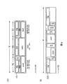
Fig. 1 (A) expression is as the integrated circuit (IC) apparatus 500 of the comparative example of present embodiment.The integrated circuit (IC) apparatus 500 of Fig. 1 (A) comprises storage block MB (video data RAM) and data driving block DB.And storage block MB and data driving block DB dispose along the D2 direction.In addition, storage block MB, data driving block DB's is in a ratio of long super flat piece along the length of D1 direction and width in the D2 direction.
View data from host computer side is written into storage block MB.Then, data driving block DB is transformed to the data voltage of simulation to the Digital Image Data of writing into storage block MB, drives the data line of display panel then.Like this, picture signal stream is the D2 direction in Fig. 1 (A).Therefore, in Fig. 1 (A) comparative example, according to this signal flow, storage block MB and data driving block DB dispose along the D2 direction.So, between the input and output short path, can optimize the delay of signal, can the good signal of transfer efficiency.
Yet,, have following technological deficiency for the comparative example of Fig. 1 (A).
The first, with regard to integrated circuit (IC) apparatus such as driver,, require the size of dwindling chip for cost degradation., if adopt microfabrication, and, be not only short side direction, and company commander's edge direction is also reduced by dwindling integrated circuit (IC) apparatus 500 merely to dwindle chip size.So, cause the installation difficult technologies defective shown in Fig. 2 (A).That is to say that even preferably export spacing for example more than or equal to 22 μ m,, because the spacing after the dwindling merely as Fig. 2 (A) shown in for example has only 17 μ m, spacing is too narrow, becomes difficult so install.Moreover the instrument bezel of display panel broadens, and the peek of glass reduces, and causes cost to increase.
The second, in display driver, according to technical specification of kind (amorphism TFT, low temperature polycrystalline silicon TFT), pixel count (QCIF, QVGA, VGA) and the product of display panel etc., the formation of storer and data driver changes to some extent.So, with regard to the comparative example of Fig. 1 (A), even the product that has is shown in Fig. 1 (B), the unit interval of its solder pad space length, storer is consistent with the unit interval of data driver, as long as the formation of storer and data driver changes, shown in Fig. 1 (C), their spacing is also just inconsistent.And, shown in Fig. 1 (C),, between circuit block,, have to form unnecessary distribution zone in order to absorb the inconsistent of spacing if spacing is inconsistent.Particularly, for the comparative example that at D1 direction piece is flat Fig. 1 (A), it is bigger to be used to absorb the inconsistent unnecessary distribution of spacing zone.Consequently, the width W of the D2 direction of integrated circuit (IC) apparatus 500 increases, and chip area increases, and causes the increase of cost.
On the other hand, for fear of this class state of affairs, for solder pad space length and unit interval being evened up change the layout of storer and data driver, this causes the construction cycle to prolong again, and the result causes cost to increase.That is to say that for the comparative example of Fig. 1 (A), the circuit of each circuit block constitutes and layout all designs separately, adjust the operation of spacing again, thereby generate unnecessary dummy section, and cause designing problem such as poor efficiencyization.
2. the formation of integrated circuit (IC) apparatus
Fig. 3 illustrates the formation of the integrated circuit (IC) apparatus 10 of the present embodiment that can solve above-mentioned technological deficiency.With regard to present embodiment, from the minor face of integrated circuit (IC) apparatus 10 promptly the first limit SD1 towards the direction of the 3rd limit SD3 on opposite as first direction D1, the opposite direction of D1 as third direction D3.From the long limit of integrated circuit (IC) apparatus 10 promptly the second limit SD2 towards the direction of the 4th limit SD4 on opposite as second direction D2, the opposite direction of D2 as the four directions to D4.In addition, in Fig. 3, though the left side of integrated circuit (IC) apparatus 10 is the first limit SD1, the right is the 3rd limit SD3,, also can be that the left side is that the 3rd limit SD3, the right are the first limit SD1.
As shown in Figure 3, the integrated circuit (IC) apparatus 10 of present embodiment comprises along the first~the N the circuit block CB1~CBN (N is the integer more than or equal to 2) of D1 direction configuration.That is in the comparative example of Fig. 1 (A), circuit block is arranged along the D2 direction, and in the present embodiment, circuit block CB1~CBN arranges along the D1 direction.And each circuit block is super flat piece unlike the comparative example of Fig. 1 (A), but relatively near square piece.
In addition, integrated circuit (IC) apparatus 10 is included in the D2 direction side of circuit block CB1~CBN of the first~the N along outgoing side I/F zone 12 (broad sense is first interface area) that limit SD4 is provided with.And comprise the input side I/F zone 14 (broad sense is second interface area) that is provided with along limit SD2 in the D4 direction side of the first~the N circuit block CB1~CBN.More particularly, outgoing side I/F zone 12 (first I/O district) is configured in D2 direction one side of circuit block CB1~CBN, and not by for example other circuit block.And input side I/F zone 14 (second I/O district) also directly is not configured in D4 direction one side of circuit block CB1~CBN by for example other circuit block.That is only there is a circuit block (data driving block) in the part that exists in data driving block in the D2 direction at least.In addition, in that (Intellectual Property: intellecture property) core is used, and when being assembled in other integrated circuit (IC) apparatus, also can form the formation that is not provided with in the I/F zone 12,14 at least one as IP integrated circuit (IC) apparatus 10.
Outgoing side (display panel side) I/F zone 12 is and display panel forms the zone of interface, and the output that comprise pad, is connected in pad is with various elements such as transistor and protecting components.Specifically, comprise to the data line outputting data signals, to the output of sweep trace output scanning signal with transistor etc.In addition, when display panel is touch panel etc., also can comprise the input transistor.
Input side (host computer side) I/F zone 14 is and main frame (MPU, image process controller, baseband engine) forms the zone of interface, and input (I/O with) transistor, output that can comprise pad, is connected in pad is with various elements such as transistor and protecting components.Specifically, the input that comprises the signal (digital signal) that is used to import from main frame with transistor, be used for to the output of main frame output signal with transistor etc.
In addition, also can be provided with along minor face is outgoing side or the input side I/F zone of limit SD1, SD3.In addition, also can be arranged on I/F (interface) district 12,14, also can be arranged on zone beyond it (the first~the N circuit block CB1~CBN) as the projection of external connection terminals etc.During regional beyond being located at I/ F zone 12,14, can adopt the small-sized protruding technology (is the protruding technology of core with the resin) beyond the metal bump to realize.
The first~the N circuit block CB1~CBN can comprise the circuit block (circuit block that possesses difference in functionality) that two (perhaps three) are different at least.With integrated circuit (IC) apparatus 10 is that the situation of display driver is an example, and circuit block CB1~CBN can comprise as two circuit blocks in data driver, storer, scanner driver, logical circuit, grayscale voltage generation circuit and the power circuit at least.More particularly, circuit block CB1~CBN can comprise data driving block and logic circuit block at least, and, can comprise the grayscale voltage generation circuit piece.In addition, under the situation of internal memory, can also comprise storage block.
For example, Fig. 4 represents the example of the circuit block of various types of display drivers and built-in display driver.(Thin FilmTransistor: thin film transistor (TFT)) panel is with regard to display driver, and circuit block CB1~CBN comprises storer, data driver (source electrode driver), scanner driver (gate drivers), logical circuit (gate-array circuit), grayscale voltage generation circuit (checking gamma circuit) and these circuit blocks of power circuit with regard to the amorphism TFT of internal memory (RAM).On the other hand, with regard to low temperature polycrystalline silicon (LTPS) the TFT panel of memory built-in is used display driver,, can omit the scan drive circuit piece because can on glass substrate, form scanner driver.And, can omit storage block for the non-built-in amorphism TFT panel of storer, for the non-built-in low temperature polycrystalline silicon TFT panel of storer, can omit the circuit block of storer and scanner driver.In addition, with regard to CSTN (Color Super Twisted Nematic) panel, TFD (Thin Film Diode: thin film diode) with regard to the panel, then can omit the grayscale voltage generation circuit piece.
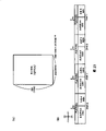
The example of the plane figure of the display-driver Ics device 10 of Fig. 5 (A), Fig. 5 (B) expression present embodiment.Fig. 5 (A), Fig. 5 (B) are the examples that the amorphism TFT panel of memory built-in is used, and for example Fig. 5 (A) is target with QCIF, 32 rank with display driver, and Fig. 5 (B) is target with QVGA, 64 rank with display driver then.
With regard to Fig. 5 (A), (B), its first~the N circuit block CB1~CBN comprises first~the 4th storage block MB1~MB4 (broad sense is the first~the I storage block, and I is the integer more than or equal to 2).Corresponding with each first~the 4th storage block MB1~MB4, comprise along the D1 direction its separately in abutting connection with the configuration first~the 4th data driving block DB1~DB4 (broad sense is the data driving block of the first~the I).Specifically, storage block MB1 and data driving block DB1 be along D1 direction disposed adjacent, storage block MB2 then with data driving block DB2 along D1 direction disposed adjacent.And data driving block DB1 is used for the storage block MB1 storage of the view data (video data) of driving data lines by adjacency, and data driving block DB2 is used for the view data of driving data lines and is then stored by the storage block MB2 of adjacency.
In Fig. 5 (A), (broad sense is the J storage block to the MB1 in storage block MB1~MB4, the DB1 (broad sense be J data driving block) of D3 direction one side of 1≤J<I) in configuration data drive block DB1~DB4.In addition, in the D1 of storage block MB1 direction one side in abutting connection with configuration store piece MB2 (broadly being the storage block of J+1).Then, in the D1 of storage block MB2 direction one side in abutting connection with configuration data drive block DB2 (broadly being the data driving block of J+1).The configuration of storage block MB3, MB4, data driving block DB3, DB4 also is the same.Like this, in Fig. 5 (A), with respect to the boundary line of MB1, MB2, MB1, DB1 and MB2, DB2 dispose symmetrically, and with respect to the boundary line of MB3, MB4, MB3, DB3 and MB4, DB4 dispose symmetrically.In addition, in Fig. 5 (A), though DB2 and DB3 in abutting connection with configuration,, not in abutting connection with and to dispose other circuit block betwixt also passable.
On the other hand, among Fig. 5 (B), for D3 direction one side of the MB1 among storage block MB1~MB4 (broadly the being the J storage block) DB1 (J data driving block) in configuration data drive block DB1~DB4.In addition, the D1 of storage block MB1 direction one side in abutting connection with the configuration DB2 (data driving block of J+1).The D1 of DB2 direction one side in abutting connection with the configuration MB2 (storage block of J+1).DB3, MB3, DB4, MB4 dispose too.In addition, though MB1 and DB2, MB2 and DB3, MB3 and DB4 are respectively in abutting connection with configuration in Fig. 5 (B),, not in abutting connection with and to dispose other circuit block betwixt also passable.
According to the configuration of Fig. 5 (A), has the advantage of (between the storage block of J, J+1) common column address decoder between storage block MB1 and MB2 and MB3 and MB4.On the other hand, according to the configuration of Fig. 5 (B), the wiring closet that can make the data-signal output line from data driving block DB1~DB4 to outgoing side I/F zone 12 has the advantage that can improve wiring efficiency apart from homogenising.
The layout of the integrated circuit (IC) apparatus 10 of present embodiment is not to be defined in Fig. 5 (A), (B).For example, the number of blocks of storage block and data driving block also can be 2,3 or more than or equal to 5, also can storage block and data driving block not carried out cutting apart of piece and is constituted.And, also can implement the non-conterminous embodiment of storage block and data driving block.And, be not fine even do not establish such formations such as storage block, scanner driver piece, power circuit piece or grayscale voltage generation circuit piece yet.Between circuit block CB1~CBN and outgoing side I/F zone 12 or input side I/F zone 14, also can be arranged on the extremely narrow circuit block (smaller or equal to the elongated circuit block of WB) of width on the D2 direction.In addition, circuit block CB1~CBN can also comprise the circuit block of different circuit blocks in the multistage arrangement of D2 direction.For example, also can be scan drive circuit and power circuit as a circuit block.
The integrated circuit (IC) apparatus 10 of Fig. 6 (A) expression present embodiment is along the example of the sectional view of D2 direction.W1, WB, W2 are respectively outgoing side I/F zone 12, circuit block CB1~CBN, input side I/F zone 14 width in the D2 direction among the figure.In addition, W is the width of integrated circuit (IC) apparatus 10 in the D2 direction.
For present embodiment, shown in Fig. 6 (A), on the D2 direction, can be not between circuit block CB1~CBN (data driving block DB) and outgoing side, input side I/ F zone 12,14, do not sandwich other circuit block and constitute.So, just can make W1+WB+W2≤W<W1+2 * WB+W2, can realize elongated integrated circuit (IC) apparatus.Specifically, the width W<2mm of D2 direction can be made, more specifically, W<1.5mm can be made.And consider the inspection and the assembling of chip, preferred W>0.9mm.In addition, the length L D of long side direction then can accomplish 15mm<LD<27mm.The shape of chip can be accomplished SP>10 than SP=LD/W, more particularly, and SP>12.
Width W 1, WB, the W2 of Fig. 6 (A) is respectively the width of the transistor formation region (body region, active region) in outgoing side I/F zone 12, circuit block CB1~CBN, input side I/F zone 14.That is the transistor of transistor and electrostatic protection element etc. is used in 12,14 formation outputs with transistor, I/O with transistor, input in the I/F zone.In addition, form the transistor of forming circuit in circuit block CB1~CBN zone.And, determine W1, WB, W2 with well region and the diffusion region that forms this transistorlike as benchmark.For example, in order to realize more elongated integrated circuit (IC) apparatus, hope is also to form projection (active face projection) on the transistor of circuit block CB1~CBN.Concrete, (active region) forms with resin and forms its core, forms the resin core projection of metal level etc. on the surface of resin on transistor.And this projection (external connection terminals) is connected on the pad that is configured in I/F zone 12,14 by metal wiring.The W1 of present embodiment, WB, W2 are not the width in the formation zone of such projection, but the width in the transistor formation region territory that below projection, forms.
The width of each comfortable D2 direction of circuit block CB1~CBN for example can be unified for wide.At this moment, as long as the width of each circuit block is identical in fact just passable, the difference that several μ m~20 μ m (tens of μ m) degree is for example arranged is in permissible range.And when having the different circuit block of width in circuit block CB1~CBN, width W B can be a maximum width in the width of circuit block CB1~CBN.The breadth extreme of this moment can be the width in the D2 direction of data driving block for example.Perhaps, under the situation of the integrated circuit (IC) apparatus of memory built-in, can be the width in the D2 direction of storage block.The dummy section of for example wide 20~30 μ m degree can be set between circuit block CB1~CBN and I/ F zone 12,14 in addition.
With regard to present embodiment, on outgoing side I/F zone 12, can be configured in the pad of the progression of D2 direction for one or more levels.So if consider pad width (for example 0.1 μ m) and solder pad space length, the width W 1 in the D2 direction in outgoing side I/F zone 12 can be accomplished 0.13mm≤W1≤0.4mm.In addition, because can be configured in the pad of the progression of D2 direction in input side I/F zone 14, so the width W 2 in input side I/F zone 14 just can be accomplished 0.1mm≤W2≤0.2mm for one or more levels.In order to realize elongated integrated circuit (IC) apparatus, need to form from the logical signal of logic circuit block, from the gray scale voltage signal of grayscale voltage generation circuit piece and the distribution of power supply by global lines on circuit block CB1~CBN, the total width of this class distribution is for example in the degree of 0.8~0.9mm.Thereby, considering these situations, the width W B of circuit block CB1~CBN can accomplish 0.65≤WB≤1.2mm.
And even W1=0.4mm, W2=0.2mm is because of 0.65≤WB≤1.2mm, so WB>W1+W2 sets up.In addition, all be under the situation of minimum value at W1, WB, W2, i.e. W1=0.13mm, WB=0.65mm, W2=0.1mm, the width of integrated circuit (IC) apparatus is W=0.88mm.So W=0.88mm<2 * WB=1.3mm sets up.At W1, WB, W2 all is under the peaked situation, W1=0.4mm, WB=1.2mm, W2=0.2mm, and then the width of integrated circuit (IC) apparatus is the degree of W=1.8mm.So W=1.8mm<2 * WB=2.4mm sets up.Therefore, relational expression W<2 * WB sets up, and can realize elongated integrated circuit (IC) apparatus.
For the comparative example of Fig. 1 (A), shown in Fig. 6 (B), dispose plural a plurality of circuit block along the D2 direction.In addition, in the D2 direction, be formed with the distribution zone between the circuit block and between circuit block and I/F zone.So integrated circuit (IC) apparatus 500 just broadens in the width W of D2 direction (short side direction), can not realize tall and thin elongated chips.Thereby even utilize microfabrication that chip is shunk, still, shown in Fig. 2 (A), because the length L D of D1 direction (long side direction) shortens, the output spacing becomes thin space, so, cause installing difficulty.
At this technological deficiency, shown in Fig. 3, Fig. 5 (A), Fig. 5 (B), in the present embodiment, dispose a plurality of circuit block CB1~CBN along the D1 direction.In addition, shown in Fig. 6 (A), can be configured in following (the active face projection) of pad (projection) to transistor (circuit component).By the global lines that the upper strata (lower floor of pad) in the local line of the inner distribution of circuit block forms, also can form between the circuit block or the signal wire between circuit block and the I/F zone etc.So, shown in Fig. 2 (B), can the width W of D2 direction be narrowed down in integrated circuit (IC) apparatus 10, realize super tall and thin elongated chips.The result is, the output spacing is for example maintained more than or equal to 22 μ m, can easily install.。
And, in the present embodiment, owing to dispose a plurality of circuit block CB1~CBN along the D1 direction, so can easily tackle the change of product specification.That is, because can be with the product of public platform design all size, so can improve design efficiency.For example in Fig. 5 (A), (B), having to increase at the pixel count of display panel or grey exponent number has under the situation about subtracting, and only needs the piece number of increase and decrease storage block and data driving block, the reading times etc. of view data just can correspondence in a horizontal scan period.In addition, though Fig. 5 (A), (B) are the amorphism TFT panel examples of memory built-in,, at the low temperature polycrystalline silicon TFT panel of exploitation memory built-in with under the situation of product, as long as from circuit block CB1~CBN, remove the scanner driver piece.And for example, under the situation of the non-built-in product of exploitation storer, as long as remove storage block.And, as mentioned above, even remove circuit block according to specification, in the present embodiment, because the influence that other circuit block is produced can be suppressed to minimum, so can improve design efficiency.
In the present embodiment, can be unified in for example width (highly) of data driving block and storage block to each circuit block CB1~CBN at the width (highly) of D2 direction.And, have under the situation of increase and decrease at the transistor of each circuit block, owing to can adjust in the length of D1 direction, design further high efficiency so can make by increasing and decreasing each circuit block.For example, in Fig. 5 (A), (B), under the situation that formation changes, number of transistors increases and decreases of grayscale voltage generation circuit piece and power circuit piece, also can come corresponding in the length of D1 direction by increase and decrease grayscale voltage generation circuit piece and power circuit piece.
In addition,, it is also conceivable that following collocation method: for example, on the D1 direction, data driving block is slenderly disposed, in the D4 of data driving block direction one side, along other a plurality of circuit blocks such as D1 direction configuration store pieces as second comparative example.But,,,, be difficult to realize tall and thin elongated chips so integrated circuit (IC) apparatus broadens in the width W of D2 direction because the data driving block of amplitude broad sandwiches between other circuit block such as storage block and the outgoing side I/F zone for this second comparative example.And, between data driving block and memory drives piece, produced unnecessary distribution zone, just enlarged width W more.Under the situation that the formation of data driving block or storage block changes, appear at inconsistent problem of spacing of explanation among Fig. 1 (B), (C), can't improve design efficiency.
As the 3rd comparative example of present embodiment, only it is also conceivable that circuit block (for example data driving block) to same function carries out cutting apart of piece and along the method for D1 direction alignment arrangements.But,,, can not realize the expansion of multiple product owing to can only make integrated circuit (IC) apparatus have same function (for example data driver function) for the 3rd comparative example.At this problem, in the present embodiment, circuit block CB1~CBN comprises the circuit block that has two difference in functionalitys at least.So, shown in Fig. 4, Fig. 5 (A), Fig. 5 (B), have the advantage that can provide corresponding to the multimachine kind integrated circuit (IC) apparatus of all kinds display panel.
3. circuit constitutes
Fig. 7 represents that the circuit of integrated circuit (IC) apparatus 10 constitutes.And the circuit of integrated circuit (IC) apparatus 10 constitutes the example that is not limited to Fig. 7, can implement various distortion.Storer 20 (video data RAM) is used for storing image data.Memory cell array 22 comprises a plurality of storage unit, stores the view data of a frame (width of cloth picture) at least.At this moment, a pixel is made of three sub-pixels (3 points) such as for example R, G, B, and each sub-pixel is for example being stored the view data of six (k positions).Row address decoder 24 (MPU/LCD row address decoder) is carried out the decoding of relevant row address and is handled the selection processing of the word line of the line storage unit of going forward side by side array 22.Column address decoder 26 (MPU column address decoder) is then carried out the decoding of relevant column address and is handled the selection processing of the bit line of the line storage unit of going forward side by side array 22.Writing/Reading circuit 28 (MPU Writing/Reading circuit) carries out the processing of view data write storage unit array 22 and reads the processing of view data from memory cell array 22.With for example with start address and end address for the rectangle on summit being come the accessing zone of define storage units array 22.That is, define accessing zone, the access of the line storage of going forward side by side with the column address of start address and the column address and the row address of row address and end address.
Logical circuit 40 (for example disposing wiring circuit automatically) generates to be used to control and shows control signal constantly and be used for control data processing control signal constantly etc.This logical circuit 40 can be formed by automatic configuration distributions such as for example gate arrays (G/A).Control circuit 42 generates various control signals, carries out the control of device integral body.Specifically, to the adjustment data (γ correction data) of grayscale voltage generation circuit 110 output gray-level characteristics (γ characteristic), and the voltage of control power circuit 90 generates.In addition, the storer that has used row address decoder 24, column address decoder 26, Writing/Reading circuit 28 is carried out the control that Writing/Reading is handled.Showing constantly that control circuit 44 generates to be used to control shows various control signals constantly, the reading of the view data of control from the storer to the display panel side.46 pairs of each visits from main frame of main frame (MPU) interface circuit generate internal pulses, realize the main interface that storer is conducted interviews.Rgb interface circuit 48 is by the rgb interface of Dot Clock realization with the RGB writing data into memory of animation.And, also can be any one the formation that only is provided with in master interface circuit 46, the rgb interface circuit 48.
In Fig. 7, conduct interviews to storer 20 with a pixel unit from master interface circuit 46, rgb interface circuit 48.On the other hand, according to showing constantly with master interface circuit 46, rgb interface circuit 48 are independently inner, each line period with the specified capable unit of row address to data driver 50 transport picture data.
Power circuit 90 is the circuit that are used to generate various supply voltages, and its formation is shown in Fig. 9 (A).Booster circuit 92 be to use boost with electric capacity, boosting boosts input supply voltage and internal power source voltage in the mode of charge pump and generates the circuit of booster voltage with transistor, can comprise 1 time~No. 4 booster circuits etc.Can generate the high voltage of scanner driver 70 and grayscale voltage generation circuit 110 uses by this booster circuit 92.Regulating circuit 94 carries out the level adjustment by the booster voltage of booster circuit 92 generations.VCOM generative circuit 96 generates the VCOM voltage and the output of the counter electrode of supplying with display panel.Control circuit 98 is used to carry out the control of power circuit 90, and it comprises various control registers etc.
Grayscale voltage generation circuit (checking gamma circuit) the 110th is used to generate the circuit of gray scale voltage, and its formation is shown in Fig. 9 (B).Select to select with voltage VS0~VS255 (broad sense is R and selects to use voltage) according to high-tension supply voltage VDDH, the VSSH output that generates by power circuit 90 with voltage generation circuit 112 (bleeder circuit).Specifically, select to comprise the ladder resistor circuit of a plurality of resistive elements with series connection with voltage generation circuit 112.And, will VDDH, VSSH voltage after partial be exported with voltage VSO~VS255 as selecting by this ladder resistor circuit.Gray scale voltage selects circuit 114 according to the adjustment data that are set in the gray-level characteristic of adjusting register 116 by logical circuit 40, from selecting, for example under the situation on 64 rank, select 64 (broadly to be S with voltage VS0~VS255, the voltage of R>S) is as gray scale voltage V0~V63 output.Like this, can generate the gray scale voltage of the preferred gray-level characteristic (γ correcting feature) that is adapted to display panel.And under the situation that reversal of poles drives, also the ladder resistor circuit used of the ladder resistor circuit that can use positive polarity and negative polarity is arranged on and selects with in the voltage generation circuit 112.In addition, the resistance of each resistive element of ladder resistor circuit also can be according to adjusting the adjustment data change that register 116 is set.It also can be the formation that impedance inverter circuit (operational amplifier that connects voltage follower) is set in selecting with voltage generation circuit 112 or gray scale voltage selection circuit 114.
Figure 10 (A) expression comprises the configuration example of each DAC (Digital Analog Converter, digital to analog converter) of the D/A change-over circuit 54 of Fig. 8 (A).Each DAC of Figure 10 (A) can be provided with by each sub-pixel (perhaps each pixel), and is made of ROM code translator etc.And, according to six bit digital view data D0~D5 and reversal data XD0~XD5 thereof from storer 20, select among the gray scale voltage V0~V63 of grayscale voltage generation circuit 110 any, thus, D0~D5 converts aanalogvoltage to view data.And, the analog voltage signal DAQ of gained (DAQR, DAQG, DAQB) is outputed to output circuit 56.
Display driver of using for low temperature polycrystalline silicon TFT etc., R is carried out being delivered to after the multipath conversion with data-signal with, B with, G under the situation of display driver (under the situation of Figure 10 (C)), can carry out D/A conversion with, G with the pictorial data that, B uses to R with a public DAC.In this case, each DAC of Figure 10 (A) is provided with by each pixel.
Figure 10 (B) illustrates the formation of each contained output SQ of the output circuit 56 of Fig. 8 (A).Each output SQ of Figure 10 (B) can be provided with by each pixel.Each output SQ comprises R (red) usefulness, G (green) usefulness, B (indigo plant) impedance inverter circuit OPR, OPG, OPB (operational amplifier that connects voltage follower), carry out signal DAQR, the DAQG from DAC, the impedance conversion of DAQB, and data-signal DATAR, DATAG, DATAB are outputed to R, G, B data-signal output line.For example under the situation of low temperature polycrystalline silicon TFT panel, on-off element (switch transistor) SWR, SWG, SWB shown in Figure 10 (C) also can be set, and the data-signal DATA behind the data-signal that multiplexing R uses, G uses, B uses is exported by impedance inverter circuit OP.In addition, also can be in a plurality of pixels the multiplex data signal.And, can also be the impedance inverter circuit shown in Figure 10 (B), (C) not to be set and the formation of only establishing on-off element etc. at output SQ.
4. overall distribution
4.1 overall wiring method
For the miniature elongated integrated circuit (IC) apparatus that realizes that Fig. 2 (B) is such, need dwindle the width W of integrated circuit (IC) apparatus on the D2 direction.For reduced width W, need again efficiently to signal wire, power lead distribution between the circuit block that disposes along the D1 direction.Therefore, in the present embodiment,, the signal wire between these circuit blocks, power lead are carried out distribution by overall wiring method.
For example, in Figure 11, the first~the N circuit block CB1~CBN is provided with outgoing side I/F zone 12 (first interface area) along the configuration of D1 direction in D2 direction side, is provided with input side I/F zone 14 in its D4 direction side.And, circuit block CBM, the CBM+1 among circuit block CB1~CBN, CBM+2 (1≤M≤N-2) in abutting connection with configuration.In the present embodiment, like this in abutting connection with between circuit block CBM, the CBM+1 of configuration and/or between CBM+1, the CBM+2, at the LL1 of local line, LL2 that the wiring layer (for example first~the 4th aluminum wiring layer ALA, ALB, ALC, ALD) of I (I be the integer more than or equal to 3) layer lower floor is gone up formation as at least a among both of signal wire and power lead by distribution.
On the other hand, between the circuit block of the not adjacency in circuit block CB1~CBN, wiring layer more than the I layer (for example, the 5th aluminum wiring layer ALE) global lines of Xing Chenging is as at least a among both of signal wire and power lead, along D1 direction distribution on the circuit block between the circuit block of adjacency not.For example, among Figure 11, logic circuit block LB not with circuit block CBM, CBM+1, CBM+2 adjacency.Therefore, between logic circuit block LB and circuit block CBM, CBM+1, CBM+2, the global lines GLL that distribution for example forms at aluminum wiring layer ALE etc. is to provide the signal from LB.And, in Figure 11, power circuit piece PB not with circuit block CBM, CBM+1, CBM+2 adjacency.Therefore, between power circuit piece PB and circuit block CBM, CBM+1, CBM+2, the global lines GLP that distribution for example forms at aluminum wiring layer ALE etc. is to provide the power supply from PB.
The concrete distribution example of global lines shown in Figure 12 (A), (B).In Figure 12 (A), circuit block CB1~CBN comprises: be used for data driving block DB1, the DB2 of driving data lines and the logic circuit block LB of control DB1, DB2.And, also comprise the gray scale voltage generative circuit piece GB that generates gray scale voltage.The driver that is used for offering data driving block DB1, DB2 from the driver control signal of logic circuit block LB with global lines GLD along D1 direction distribution at the circuit block between logic circuit block LB and data driving block DB1, DB2.The GTG that is used for offering data driving block DB1, DB2 from the gray scale voltage of gray scale voltage generative circuit piece GB with global lines GLG along D1 direction distribution at the circuit block between gray scale voltage generative circuit piece GB and data driving block DB1, DB2.And in abutting connection with configuration, distribution is used for the LLG of local line that LB offers the adjustment data of GTG GB between logic circuit block LB and gray scale voltage generative circuit piece GB along the D1 direction for gray scale voltage generative circuit piece GB and logic circuit block LB.
In Figure 12 (B), circuit block CB1~CBN comprises that data driving block DB1, DB2 and storage offer storage block MB1, the MB2 of the view data of DB1, DB2.The storer that is used for offering storage block MB1, MB2 from the write data signal at least (perhaps address signal, storer control signal) of logic circuit block LB with global lines GLM along D1 direction distribution at the circuit block between logic circuit block LB and storage block MB1, MB2.But also distribution is used for the driver control signal from logic circuit block LB is offered the driver global lines GLD of data driving block DB1, DB2.In abutting connection with configuration, distribution is used for MB1 between storage block MB1 and data driving block DB1 provides the local line LLM1 of view data to DB1 along the D1 direction for data driving block DB1, DB2 and storage block MB1, MB2.Distribution is used for MB2 between storage block MB2 and data driving block DB2 provides the local line LLM2 of view data to DB2.
Shown in Fig. 9 (B), gray scale voltage generative circuit 110 comprises adjusts register 116.40 pairs of these adjustment registers 116 of the logical circuit of Fig. 7 are provided for the adjustment data of the amplitude adjustment of gray scale voltage and the fine setting of gray-level characteristic (slope adjustment etc.).If carry out this adjustment, can obtain and the corresponding only gray-level characteristic of the kind of display panel, thereby improve display quality.
But the figure place of adjustment data that is used to carry out this adjustment is very many.Therefore, the bar number of the signal wire of distribution is also very many between the logic circuit block LB of Figure 12 (B) and gray scale voltage generative circuit piece GB.
Therefore, in Figure 12 (B), along the D1 direction in abutting connection with configuration logic piece LB with gray scale voltage generative circuit piece GB.And then distribution is used for LB between logic circuit block LB and gray scale voltage generative circuit piece GB provides the local line LLG of the adjustment data of GTG to GB.
And in Figure 12 (B), for example data driving block DB1 receives the view data that is stored among the storage block MB1, carries out the D/A conversion of this view data etc., and drives the data line of display panel.So the figure place of the view data that provides from storage block MB1 is very many.Therefore, the bar number of the signal wire of distribution is also very many between data driving block DB1 and storage block MB1.
Therefore, in Figure 12 (B), along the D1 direction in abutting connection with configuration data drive block DB1, DB2 and storage block MB1, MB2.And then distribution is used for MB1, MB2 provide view data to DB1, DB2 the LLM1 of local line, LLM2 between data driving block DB1, DB2 and storage block MB1, MB2.
Like this, in the present embodiment, as logic circuit block LB and gray scale voltage generative circuit piece GB and data driving block DB1, DB2 and storage block MB1, MB2, the circuit blocks that the bar number of the signal wire of distribution between circuit block is a lot of are in abutting connection with configuration.And, between the circuit block of these adjacency, distribution at the wiring layer of wiring layer (ALE) lower floor of global lines (LLG of local line, LLM1, the LLM2 of ALA~ALD) form.So, connect with shortest path between the circuit block of these adjacency, thereby can prevent the increase of the chip area that causes because of the distribution zone.
On the other hand, distribution between logic circuit block LB and data driving block DB1, the DB2 or the bar number of the signal wire between logic circuit block LB and storage block MB1, the MB2 than the bar number of local line LLG, LLM1, LLM2 still less.And the circuit block that also has other is between logic circuit block LB and DSB data store block DB1, DB2, storage block MB1, MB2.
Therefore, in the present embodiment, will (the global lines GLD that the wiring layer on upper strata of ALA~ALD) forms, GLM distribution be between logic circuit block LB and data driving block DB1, DB2, storage block MB1, MB2 at the LLG of local line, LLM1, LLM2.So, even distribution under the very many situations of the distribution strip number of the LLM1 of local line, LLM2 between the circuit block of adjacency, also can be at the upper strata of the LLM1 of these local lines, LLM2 distribution global lines GLD, GLM.Therefore, can be on circuit block CB1~CBN the global lines of many of distribution, thereby improve wiring efficiency.That is, because can pass through a lot of signal wire of global lines distribution, so can reduce around the bar number of circuit block distribution at the signal wire in outgoing side I/F zone 12 or input side I/F zone 14.Finally, can dwindle the width W of integrated circuit (IC) apparatus on the D2 direction, realize the so miniature elongated chips of Fig. 2 (B).
4.2 the distribution of the global lines on buffer circuit, the row address decoder
Global lines shown in Figure 13 is the distribution example more specifically.In Figure 13, be used for the driver control signal from logic circuit block LB is offered driver global lines GLD distribution on buffer circuit BF1~BF3, row address decoder RD1~RD3 of data driving block DB1~DB3.That is, begin roughly in line distribution from logic circuit block LB with global lines GLD on buffer circuit BF1~BF3 and row address decoder RD1~RD3 along the D1 direction at the driver that forms as the 5th aluminum wiring layer ALE of top metal.The driver control signal that is provided with global lines GLD by these drivers outputs to the data driver DR1~DR3 of the D2 direction side that is configured in buffer circuit BF1~BF3 by behind buffer circuit BF1~BF3 buffer memory.
And, in Figure 13, be used for the write data signal at least (perhaps address signal, storer control signal) from logic circuit block LB is offered the storer usefulness global lines GLM of storage block MB1~MB3 along D1 direction distribution.That is, the storer that forms at the 5th aluminum wiring layer ALE begins distribution along the D1 direction from logic circuit block LB with global lines GLM.
More specifically, in Figure 13, dispose forwarding piece RP1~RP3 corresponding to storage block MB1~MB3.These transmit piece RP1~RP3 comprise with behind write data signal at least (perhaps address signal, the storer control signal) buffer memory from logic circuit block LB, export to the impact damper of storage block MB1~MB3.As shown in figure 13, storage block MB1~MB3 with transmit piece RP1~RP3 along the D1 direction in abutting connection with configuration.
For example, when using storer will offer storage block MB1~MB3 from write data signal, address signal, the storer control signal of logic circuit block LB with global lines GLM, if not with these signal buffer memorys, the rising waveform of signal or falling waveform can die down so.As a result, cause that easily data write the time lengthening of storage block MB1~MB3, and write error perhaps takes place.
About this point, if image pattern 13 like this, to transmit piece RP1~RP3 in abutting connection with for example D1 direction side that is configured in each storage block MB1~MB3, then these write data signals, address signal, storer control signal just by after transmitting piece RP1~RP3 buffer memory, are exported to each storage block MB1~MB3.Therefore, can alleviate the rising waveform of signal or dying down of falling waveform, realize the correct data of storage block MB1~MB3 are write.
In Figure 13, integrated circuit (IC) apparatus comprises the gray scale voltage generative circuit piece GB that generates gray scale voltage.Be used for to offer from the gray scale voltage of gray scale voltage generative circuit piece GB the GTG usefulness global lines GLG of data driving block DB1~DB3 along D1 direction distribution.That is, the GTG that forms at the 5th aluminum wiring layer ALE begins distribution along the D1 direction from logic circuit block LB with global lines GLG.The gray scale voltage supply line GSL1~GSL3 that is used for offering data driver DR1~DR3 with the gray scale voltage of global lines GLG from GTG at each data driver DR1~DR3 along D2 direction distribution.Particularly, gray scale voltage supply line GSL1~GSL3 strides across a plurality of sub-pixel driver element described later, along D2 direction distribution on the D/A converter of each sub-pixel driver element.
And then in the present embodiment, as shown in figure 13, storer usefulness global lines GLM is along D1 direction distribution between GTG is with global lines GLG and driver usefulness global lines GLD.
That is, as shown in figure 13, in the present embodiment, buffer circuit BF1~BF3 and row address decoder RD1~RD3 dispose along the D1 direction.By with driver with global lines GLD from logic circuit block LB along D1 direction distribution on these buffer circuits BF1~BF3, row address decoder RD1~RD3, can significantly improve wiring efficiency.
And, need provide gray scale voltage to data driver DR1~DR3 from gray scale voltage generative circuit piece GB, therefore GTG is carried out distribution with global lines GLG along the D1 direction.
On the other hand, provide address signal, storer control signal etc. with global lines GLM to row address decoder RD1~RD3 by storer.Therefore, near preferred storer global lines GLM distribution row address decoder RD1~RD3.
About this point, in Figure 13, storer uses global lines GLM at GTG global lines GLG and driver distribution between the global lines GLD.Therefore, can will offer row address decoder RD1~RD3 with the address signal of global lines GLM, storer control signal etc. from storer with the shortest path.And, GTG with global lines GLG along the D1 direction roughly in line distribution at the upside of this storer with global lines GLM.Therefore, use layer of aluminum wiring layer ALE just can not make global lines GLG, GLM, GLD carry out distribution across, thereby can improve wiring efficiency.
4.3 forwarding piece
Transmit the configuration example of piece shown in Figure 14.In Figure 14, behind impact damper BFA1 by constituting of the write data signal (WD0, WD1...) of logic circuit block LB, BFA2... buffer memory, output to the forwarding piece of next stage by 2 phase inverters.Particularly, in Figure 13, the signal behind buffer memory is transmitted piece RP2 output from the forwarding piece RP1 of the D1 direction side that is configured in storage block MB1 to the next stage of the D1 direction side that is configured in storage block MB2.From the write data signal of logic circuit block LB by impact damper BFB1, BFB2... buffer memory after, output to storage block.Particularly, in Figure 13, the signal behind buffer memory is exported to storage block MB1 from the forwarding piece RP1 of the D1 direction side that is configured in storage block MB1.Like this, in the present embodiment,, not only be provided with the impact damper BFA1, the BFA2... that are used for to the storage block output of next stage, but also be provided with impact damper BFB1, the BFB2... that each storage block is used for write data signal.By this design, can prevent effectively since the parasitic capacity of the storage unit of storage block former thus cause write data signal waveform die down and the write time prolongs and write error etc. takes place.
And, behind impact damper BFC1... buffer memory, output to the forwarding piece of storage block and next stage from the address signal (CPU column address, CPU row address, LCD row address etc.) of logic circuit block LB.And behind impact damper BFD1... buffer memory, output to the forwarding piece of storage block and next stage from the storer control signal (read/write switching signal, CPU enable signal, bank selection signal etc.) of logic circuit block LB.
And, in the forwarding piece of Figure 14, also be provided with the impact damper of using from the reading data signal of storage block.Particularly,, and select this storage block if activate bank selection signal BANKM (H level), then from the reading data signal of this storage block behind impact damper BFE1, BFE2... buffer memory, export to read data line RD0L, RD1L....On the other hand, if do not activate bank selection signal BANKM (L level), the output state of impact damper BFE1, BFE2... is a high impedance status so.Thus, can be suitably the reading data signal of other storage block of having activated from bank selection signal be exported to logic circuit block LB.
4.4 the configuration of power circuit, logical circuit, scanner driver
Among Figure 15, the circuit block CB1~CBN that disposes on the D1 direction comprises: the power circuit piece PB, data driving block DB1, DB2 and the logic circuit block LB that generate supply voltage.Comprise turntable driving piece SB1, SB2 in addition.
In Figure 15, the power supply that is used for the supply voltage that power circuit piece PB generates is offered data driving block DB1, DB2 and logic circuit block LB with global lines GPD, GPL along D1 direction distribution between between PB and DB1, the DB2 or the circuit block between PB and the LB.
Promptly, the circuit of display driver in the LV zone (broadly, first circuit region) or MV zone (broadly, the second circuit district) etc. go up and form, wherein, the LV area configurations has (the Low Voltage with LV, low-voltage) voltage level (circuit of) power work broadly, first voltage level, the MV area configurations has to be higher than the MV (MiddleVoltage of LV, the middle pressure) circuit of the power work of voltage level (broadly, second voltage level).For example, the circuit of logic circuit block and storage block forms in the LV zone.And the circuit of D/A converter that data driving block had and operational amplifier forms in the MV zone.Therefore, be assembled in the supply voltage that power circuit piece in the display driver need generate these LV or MV, offer each circuit block again.
In this case, if only use the 14 pairs of power leads in outgoing side I/F zone 12 or input side I/F zone to carry out distribution, just be difficult in these zones 12,14 other signal wire of distribution more so, thereby cause wiring efficiency to reduce.And, if carry out distribution, there is the possibility that source impedance rises, the power supply supply capacity descends so again around power lead.
Therefore, in the present embodiment, signal wire and power lead all carry out distribution with global lines.For example, in Figure 15, use power supply to provide the MV of power circuit piece PB generation or the power supply of LV to data driving block DB1, DB2 with global lines GPD.The power work of the MV that bases such as the D/A converter in data driving block DB1, the DB2, operational amplifier provide.And the power work of the LV that the bases such as latch cicuit in data driving block DB1, the DB2 provide.And, in Figure 15, use power supply that the power supply of the LV of power circuit piece PB generation is provided to logic circuit block LB with global lines GPL.So, even the outside does not provide digital power, the power supply of the LV that logic circuit block LB also can provide with power circuit piece PB carries out work.
In Figure 15, because the global lines GPD, the GPL that begin from power circuit piece PB roughly in line distribution on data driving block DB1, DB2, logic circuit block LB, so the rising of source impedance can be suppressed for minimum, stable power is supplied with becomes possibility.
And in Figure 15, data driving block DB1, DB2 are configured between power circuit piece PB and the logic circuit block LB.In addition, in Figure 15, the two ends of integrated circuit (IC) apparatus dispose turntable driving piece SB1, SB2.That is, turntable driving piece SB1 is configured in the D1 direction side of logic circuit block LB, and turntable driving piece SB2 is configured in the D3 direction side of power circuit piece PB.
Like this turntable driving piece SB1, SB2 are being configured under the situation at integrated circuit (IC) apparatus two ends, will considering wiring efficiency when the scanner driver of wishing output is had a sweep signal also is configured in the two ends of integrated circuit (IC) apparatus with pad.On the other hand, data driving block DB1, DB2 are configured near the central portion of integrated circuit (IC) apparatus.Therefore, the data driver of wishing output is had a data-signal will be considered wiring efficiency with pad configuration near the central portion of integrated circuit (IC) apparatus the time.
Therefore, in Figure 15, scanner driver is arranged on the two ends in outgoing side I/F zone 12 with the configuring area of pad, data driver is arranged on these scanner drivers with between the pad configuration district with the configuring area of pad.By adopting this design, can be efficiently the output line of the output line of turntable driving piece SB1, SB2 and data driving block DB1, DB2 be connected to scanner driver with the pad in pad configuration district and the data driver pad with the pad configuration district.
Especially, in Figure 15, the both sides that power circuit piece PB that circuit area is big and logic circuit block LB are configured in data driving block DB1, DB2.So, the zone (zone shown in B1, the B2) of vacating that can effectively apply flexibly the D2 direction side of big power circuit piece PB of these circuit areas and logic circuit block LB forms scanner driver pad configuration district.Therefore, can improve the wiring efficiency on the outgoing side I/F zone 12, and dwindle the width W of integrated circuit (IC) apparatus on the D2 direction, realize miniature elongated integrated circuit (IC) apparatus.
4.5 shielding line
Near piece SB1 of turntable driving shown in Figure 16 and the logic circuit block LB detailed placement.In Figure 16, on logic circuit block LB, begin to be wired to the scanner driver pad in outgoing side I/F zone 12 with global lines GLS1 as the scanner driver of the output line of turntable driving piece SB1 from turntable driving piece SB1.In addition, near the detailed placement piece SB2 of turntable driving shown in Figure 17 and the power circuit piece PB.In Figure 17, on power circuit piece PB, begin to be wired to the scanner driver pad in outgoing side I/F zone 12 with global lines GLS2 as the scanner driver of the output line of turntable driving piece SB2 from turntable driving piece SB2.
In Figure 16, Figure 17, scanner driver is a lot of with the number of pad, and the bar number of the output line of turntable driving piece SB1, SB2 is also a lot.Therefore, scanner driver is also very big with the shared area in the distribution zone of global lines GLS1, GLS2.As a result, in Figure 16, Figure 17, scanner driver is forming with very wide scope on the logic circuit block LB and on the power circuit piece PB with the distribution zone of global lines GLS1, GLS2.
And the output transistor of turntable driving piece SB1, SB2 is in the such high power supply voltage of for example 30V (HV) work down.Therefore, as Figure 16, shown in Figure 17, if with scanner driver with global lines GLS1, GLS2 distribution on logic circuit block LB and/or power circuit piece PB the time, scanner driver passes through parasitic coupling capacitance with the caused noise of variation of the voltage level of global lines GLS1, GLS2, is sent on the circuit or signal wire in logic circuit block LB and/or the power circuit piece PB.As a result, may cause problems such as circuit maloperation.
Therefore, in the present embodiment, on logic circuit block LB and/or power circuit piece PB, with the lower floor of shielding line distribution at scanner driver global lines GLS1, GLS2.Particularly, as scanner driver global lines GLS1, when GLS2 forms at the 5th aluminum wiring layer ALE, distribution is at the shielding line of the formation such as the 4th aluminum wiring layer ALD of its lower floor.
The layout example of shielding line shown in Figure 18.In Figure 18, the scanner driver that begins from turntable driving piece SB1 passes through logic circuit block LB with global lines GLS1, is wired to scanner driver pad Pn, Pn+1, Pn+2....At logic circuit block LB, shielding line SDL1, SDL2, SDL3 distribution are in the lower floor of these scanner drivers with global lines GLS1.If carry out the distribution of shielding line like this, can prevent that noise that scanner driver causes with the variation of the voltage level of global lines GLS1 is sent on the circuit and/or signal wire in the logic circuit block LB by coupling capacitance.Therefore, can prevent the circuit maloperation.
In addition, in the present embodiment, shown in Figure 11, Figure 12 (A), Figure 12 (B), in the time of between with the circuit block of global lines distribution, on the circuit block between the circuit block of adjacency not, with the lower floor of shielding line distribution in global lines in adjacency not.For example, in Figure 12 (B), distribution GTG global lines GLG between the gray scale voltage generative circuit piece GB of adjacency not and data driving block DB1.At this moment, between the gray scale voltage generative circuit piece GB and the circuit block between the data driving block DB1 of adjacency not, be on the storage block MB1, with the lower floor of shielding line distribution at global lines GLG.Particularly, with the shielding line distribution between the bit line and global lines GLG of storage block MB1.
If promptly distribution GTG global lines GLG on storage block MB1 may produce following problem so.For example, in Figure 19 (A), word line WL activates, and the voltage level of bit line BL is higher than the voltage level of bit line XBL, thereby the output SAQ of sensor amplifier exports normal logical one.
To this, in Figure 19 (B), because the voltage level of global lines GLG changes, so the voltage level of XBL according to the coupling capacitance between the bit line XBL of GLG and its lower floor variation has taken place.Therefore, the logical zero that the output SAQ of sensor amplifier may output abnormality.
Therefore, in the present embodiment, on storage block, at lower floor's distribution shielding line of bit line, in the GTG global lines of the upper strata of shielding line distribution from gray scale voltage generative circuit BOB(beginning of block).
For example, shown in Figure 20 (A) under the situation of lateral type unit, the distribution example of shielding line SDL.In Figure 20 (A), the undermost first aluminum wiring layer ALA is used for node and connects, and the second aluminum wiring layer ALB on its upper strata is used for the power lead of bit line BL, XBL and VDD.The 3rd aluminum wiring layer ALC is used for the power lead of word line WL and VSS, and the 4th aluminum wiring layer ALD is used to be connected to the shielding line SDL of VSS.The 5th aluminum wiring layer ALE of the superiors is used for global lines GLG (gray scale voltage output line).
Shown in Figure 20 (B) under the situation of longitudinal type unit, the distribution example of shielding line SDL.In Figure 20 (B), ALA is used for node and connects, and ALB is used for word line WL and VDD power lead.ALC is used for the power lead of bit line BL, XBL and VSS, and ALD is used for shielding line SDL.ALE is used for global lines GLG.
In Figure 20 (A), (B), bit line BL, XBL are together along D1 direction (long side direction of integrated circuit (IC) apparatus) distribution, and shielding line SDL and bit line BL, XBL are overlapping like this along D1 direction distribution.That is, shielding line SDL forms on the upper strata of bit line BL, XBL, and covers BL, XBL.
So, can the variation of the voltage level of global lines GLG be shielded by the situation that coupling capacitance is sent to bit line BL, XBL.Therefore, the voltage level that can prevent bit line BL, XBL changes and makes the output of sensor amplifier mistake.
In addition, shown in Figure 20 (A), (B), if at each storage unit distribution shielding line SDL, then shielding line SDL is not the β distribution, but is formed with the gap between shielding line.By forming such gap, can breathe freely between metal level and dielectric film, be expected to improve reliability and yield rate.
In Figure 20 (B), the power lead of the gap location distribution VSS between adjacent shielding line SDL.So, to shielding realizes by shielding line SDL upward, and horizontal shielding realizes by the power lead of VSS, thereby can shield effectively.
4.6 the configuration of logical circuit, gray scale voltage generative circuit
The detailed placement example of the LB of logic circuit block shown in Figure 21, gray scale voltage generative circuit piece GB.In Figure 21, logic circuit block LB and gray scale voltage generative circuit piece GB be the adjacency configuration on the D1 direction.In Figure 21, also be provided with buffer circuit BFL.This buffer circuit BFL comprises impact damper, is used for carrying out buffer memory from logic with the signal (logical signal) of pad, and wherein, logic uses pad configuration in input side I/F zone 14 (second interface area).In Figure 21, this buffer circuit BFL is configured in the D4 direction side of logic circuit block LB and gray scale voltage generative circuit piece GB.From logic with pad to the global lines GLBF of buffer circuit BFL along D1 direction distribution on input side I/F zone 14.
Logic circuit block LB operates under the power supply of LV voltage level (first voltage level).Buffer circuit BFL comprises being the level shifter of LV voltage level with the voltage of signals level conversion of pad from logic.If design this level shifter,, can be the voltage level of LV also with this I/O power source voltage level conversion even under the LV of the logic circuit block LB power source voltage level situation different with the I/O power source voltage level in input side I/F zone 14.Thus, can offer logic circuit block LB again with after being the voltage level of LV from logic with the voltage level conversion of the input signal of pad.
As mentioned above, it is very many to be used for the figure place of the adjustment data that GTG adjusts.Therefore, in Figure 21, in abutting connection with configuration the time, also distribution is used to provide the LLG of local line that adjusts data between LB and GB with logic circuit block LB and gray scale voltage generative circuit piece GB.
On the other hand, display driver comprises interfaces such as MPU interface, rgb interface, and also very many with the input signal of pad from logic.Therefore, need and to be connected to logic circuit block LB from logic with most of input signals of pad.
Therefore, in Figure 21, the D4 direction side that is produced in the time of can effectively applying flexibly in abutting connection with configuration logic piece LB and gray scale voltage generative circuit piece GB vacate the zone, in this vacates the zone, dispose buffer circuit BFL.That is, buffer circuit BFL is configured in the D4 direction side of logic circuit block LB and gray scale voltage generative circuit piece GB.
If adopt this configuration, so respectively with buffer circuit BFL, logic circuit block LB, when the width of gray scale voltage generative circuit piece GB on the D1 direction is made as WBF, WLB, WGB, the relation of WBF=WLB+WGB is set up.That is, can make buffer circuit BFL be wider than the width W LB of logic circuit block LB on the D2 direction at the width W BF on the D2 direction.Thus, do not take too many distribution zone and just can will be input among the buffer circuit BFL, thereby can improve wiring efficiency from most of signals of logic with pad.
That is,, then be difficult to and be connected to buffer circuit BFL from logic with most of input signals of pad if the width W LB of the width W BF of buffer circuit BFL and logic circuit block LB is roughly suitable.About this point, in Figure 21, owing to widened the width W BF of buffer circuit BFL, thereby, just most input signal can be connected to buffer circuit with the little simple layout in distribution zone, improved positioning efficiency.
In addition, integrated circuit (IC) apparatus shown in Figure 22 is along the variation of the sectional view of D2 direction.In Figure 22, at the pad lower floor configuration ESD element (electrostatic protection element) in outgoing side I/F zone 12, the output transistor of scanner driver etc.Pad lower floor in input side I/F zone 14 disposes the boost transistor of ESD element, power circuit etc.In Figure 22, the periphery of pad also is provided with the distribution zone.Particularly, the periphery of pad is used the power lead that distribution forms at the aluminum wiring layer as overall distribution area.So, even, also can utilize the overall distribution area distribution power lead of pad periphery, can improve wiring efficiency with this wiring layer of pad lower floor not being used under the situation of power lead owing to the existence of for example ESD element.
5.1 piece is cut apart
Shown in Figure 23 (A), display panel is the QVGA panel of pixel count HPN=240 of pixel count VPN=320, the horizontal scan direction (scan-line direction) of vertical scanning direction (data line direction).In addition, R, G, the B of the figure place PDB of the image of a pixel part (demonstration) data respectively are 6, and the PDB=18 position.In the case, a frame of display panel shows figure place VPN * HPN * PDB=320 * 240 * 18 of needed view data.So the storer of integrated circuit (IC) apparatus needs to store 320 * 240 * 18 view data at least.And data driver is exported each horizontal scan period (time of a sweep trace scanning) HPN=240 single data signal (corresponding to the data-signal of 240 * 18 view data) to display panel.
And in Figure 23 (B), data driver is divided into DBN=4 data drive block DB1~DB4.And storer also is divided into MBN=DBN=4 storage block MB1~MB4.That is for example four driver macroelement DMC1, DMC2, DMC3, the DMC4 that data driving block, storage block, pad piece are carried out macroelementization disposes along the D1 direction.So each driver piece DB1~DB4 exports HPN/DBN=240/4=60 single data signal in each horizontal scan period to display panel.In addition, each storage block MB1~MB4 storage (view data of VPN * HPN * PDB)/MBN=(320 * 240 * 18)/4.
5.2 repeatedly reading of a horizontal scan period
In Figure 23 (B), each data driving block DB1~DB4 is at the data-signal of 60 of horizontal scan period outputs (if R, G, B is 3, then 60 * 3=180 root).So each horizontal scan period must read 240 view data corresponding to data-signal from the storage block MB1~MB4 corresponding to DB1~DB4.
Yet, if the figure place of the view data that each horizontal scan period reads increases, storage unit (sensor amplifier) number of arranging on the D2 direction will take place to need to increase.Consequently, the width W of integrated circuit (IC) apparatus D2 direction increases, and overslaugh makes chip tall and thin.In addition, bring that word line WL is elongated, the problem of the signal delay of WL.
So in the present embodiment, adopt following method: a horizontal scan period, the view data that will be stored in each storage block MB1~MB4 from each storage block MB1~MB4 many times (RN time) reads data driving block DB1~DB4.
For example, in Figure 24, shown in A1, A2, a horizontal scan period, only at RN=2, storage access signal MACS (signal is selected in word select) is for activating (high level).Thus, a horizontal scan period, RN=2 time from each storage block to each data driving block reads image data.Like this, the contained data-latching circuit of first, second data driver DRa, DRb that is arranged at the Figure 25 in the data driving block latchs the view data that reads according to latch signal LATa, the LATb shown in A3, the A4.And, the D/A conversion of the view data that the contained D/A change-over circuit of first, second data driver DRa, DRb then is latched, the contained output circuit of DRa, DRb exports data-signal DATAa, DATAb by D/A conversion gained to the data-signal output line shown in A5, A6.Afterwards, shown in A7, the sweep signal SCSEL of grid of TFT of each pixel that is input to display panel is for activating, and data-signal is input to each pixel, and is kept.
And in Figure 24, in first horizontal scan period, twice reads image data in same first horizontal scan period, exports data-signal DATAa, DATAb to the data-signal output line.But, also can be that at first horizontal period twice reads image data DATAa, DATAb and latch, in ensuing second horizontal period, data-signal DATAa, the DATAb of the view data that correspondence is latched export the data-signal output line to.In addition, the situation of expression reading times RN=2 still, also can be RN 〉=3 among Figure 24.
According to the method for Figure 24, as shown in figure 25, read view data corresponding to 30 data-signal from each storage block, each data driver DRa, DRb then export 30 data-signal.Thus, export 60 data-signal from each data driving block.So, in Figure 24, if the view data that reads corresponding to 30 data-signal from each storer by once reading gets final product.So, compare a horizontal scan period and only read once method, can reduce the storage unit of the D2 direction of Figure 25, the number of sensor amplifier.Consequently, the width of integrated circuit (IC) apparatus D2 direction can be reduced, super tall and thin elongated chips can be realized.Particularly, the length of a horizontal scan period is the level of 52 μ sec under the situation of QVGA.On the other hand, for example be the level of 40nsec the readout time of storer, compares very short with 52 μ sec.So, even in the reading times of a horizontal scan period from once being increased to repeatedly, there is no great influence for display characteristic.
And Figure 23 (A) is the display panel of QVGA (320 * 240), if make the reading times RN=4 of a horizontal scan period, also can be adapted to VGA (640 * 480) display panel, thereby can increase the degree of freedom of design.
And, also can realize that a horizontal scan period repeatedly reads with first method, that is: the many different word lines in each storage block are selected a horizontal scan period by row address decoder (word line selection circuit); Also can realize that a horizontal scan period repeatedly reads, that is: the identical word line in each storage block repeatedly be selected a horizontal scan period by row address decoder with second method; Perhaps, also can realize by the combination of first, second method.
5.3 the configuration of data driver, driver element
The examples of configurations of data driver and the contained driver element of data driver is shown in Figure 25.As shown in figure 25, data driving block is included in a plurality of data driver DRa, the DRb (the first~the m data driver) that the D1 direction is piled up.In addition, each data driver DRa, DRb comprise the individual driver element DRC1~DRC30 of a plurality of 30 (broadly being Q) again.
Storage block word line WL1a be selected and shown in the A1 of Figure 24 when storage block reads for the first time view data, the first data driver DRa latchs the view data of reading according to the latch signal LATa shown in the A3.And, be latched the D/A conversion of view data, and shown in A5, exporting the data-signal output line corresponding to the data-signal DATAa of the view data that reads for the first time like that to.
On the other hand, storage block word line WL1b be selected and shown in the A2 of Figure 24 when storage block reads secondary view data, the second data driver DRb latchs the view data of reading according to the latch signal LATa shown in the A4.And, be latched the D/A conversion of view data, and shown in A6, exporting the data-signal output line corresponding to the data-signal DATAb of the view data that reads for the second time like that to.
As mentioned above, 30 data-signal of corresponding 30 pixels of each data driver DRa, DRb output is exported 60 data-signal corresponding to 60 pixels altogether.
As shown in Figure 25, if along D1 direction configuration (accumulation) a plurality of data driver DRa, DRb, then can prevent to cause making the width W condition of enlarged of integrated circuit (IC) apparatus D2 direction owing to the size of data driver scale.In addition, data driver adopts various formations according to the type of display panel.Under these circumstances, as long as, just can arrange the data driver of various formations expeditiously according to the method for a plurality of data drivers along the configuration of D1 direction.In addition, the situation the when configured number that Figure 25 shows data driver on the D1 direction is two, but configurable number also can be more than or equal to 3.
And each data driver DRa, DRb comprise 30 (Q) driver element DRC1~DRC30 along D2 direction alignment arrangements among Figure 25.Here, driver element DRC1~DRC30 receives the view data of a pixel respectively.And, carry out the D/A conversion of the view data of a pixel, the data-signal of the corresponding pixel image data of output.Each unit of this driver element DRC1~DRC30 can comprise the latch cicuit of data, DAC (DAC of 1 pixel), Figure 10 (B) of Figure 10 (A) and the output SQ of Figure 10 (C).
And, in Figure 25, the pixel count of display panel horizontal scan direction (is being shared by a plurality of integrated circuit (IC) apparatus and is being driven under the situation of data line of display panel, the pixel count of the horizontal scan direction that each integrated circuit (IC) apparatus is born) is HPN, the piece number (piece is cut apart number) of data driving block is DBN, is IN a horizontal scan period to the input number of times of driver element input image data.And IN equals the view data reading times RN of an illustrated horizontal scan period of Figure 24.In this case, the number of the driver element DRC1~DRC30 that arranges along the D2 direction can be expressed as Q=HPN/ (DBN * IN).Under the situation of Figure 25, because HPN=240, DBN=4, IN=2, so Q=240/ (4 * 2)=30.
And, at the width (spacing) of the D2 of driver element DRC1~DRC30 direction is that the width of the D2 direction of the contained peripheral circuit part of WD, data driving block (buffer circuit, distribution zone etc.) is under the situation of WPCB, and the width W B (breadth extreme) of the D2 direction of the first~the N circuit block CB1~CBN can be expressed as Q * WD≤WB<(Q+1) * WD+WPCB.In addition, be under the situation of WPC at the width of the D2 direction of the contained peripheral circuit of storage block part (row address decoder RD, distribution zone), can be expressed as Q * WD≤WB<(Q+1) * WD+WPC.
And, the pixel count of display panel horizontal scan direction be the figure place of the view data of HPN, 1 pixel be the piece number of PDB, storage block be MBN (=DBN), be RN from the reading times of storage block reads image data a horizontal scan period.At this moment, the number P of the sensor amplifier of arranging along the D2 direction in sensor amplifier piece SAB (exporting the sensor amplifier of bit image data) can be expressed as P=(HPN * PDP)/(MBN * RN).Under the situation of Figure 25, because HPN=240, PDP=18, MBN=4, RN=2, so, P=(240 * 18)/(4 * 2)=54.And number P is the effective sensor amplifier number corresponding with the effective storage unit number, does not comprise the number of pseudo-storage unit with non-effective sensor amplifiers such as sensor amplifiers.
And when the width (spacing) of the D2 direction of each sensor amplifier that sensor amplifier piece SAB is contained was WS, the width W SAB of the D2 direction of sensor amplifier piece SAB (storage block) can be expressed as WSAB=P * WS.And when the width of the D2 direction of the contained peripheral circuit of storage block part was WPC, the width W B (breadth extreme) of the D2 direction of circuit block CB1~CBN can be expressed as P * WS≤WB<(P+PDB) * WS+WPC.
5.4 the layout of data driving block
The layout that data driving block is more detailed is shown in Figure 26 for example.In Figure 26, data driving block comprises a plurality of sub-pixel driver element SDC1~SDC180 of the data-signal of the view data that it exports a corresponding sub-pixel separately.And, with regard to this data driving block, in the time of along a plurality of sub-pixel driver element of D1 direction (along the direction on the long limit of sub-pixel driver element) configuration, also dispose a plurality of sub-pixel driver elements along D2 direction perpendicular to D1.That is sub-pixel driver element SDC1~SDC180 is the matrix form configuration.And, be used for realizing that pad that the data driving block output line is electrically connected with the data line of display panel then is configured in the D2 direction side of data driving block.
For example, the driver element DRC1 of the data driver DRa of Figure 25 is made of sub-pixel driver element SDC1, SDC2, the SDC3 of Figure 26.Here, SDC1, SDC2, SDC3 are respectively that R (red) uses, G (green) uses, the sub-pixel driver element of B (orchid) usefulness, import R, G, the B view data (R1, G1, B1) of the corresponding first single data signal from storage block.And sub-pixel driver element SDC1, SDC2, SDC3 carry out the D/A conversion to these view data (R1, G1, B1), first R, G, B data-signal (data voltage) are exported to R, G, the B pad of corresponding first data lines.
Equally, driver element DRC2 is made of sub-pixel driver element SDC4, SDC5, the SDC6 that R uses, G uses, B uses.Import R, G, the B view data (R2, G2, B2) of the corresponding second single data signal from storage block.And sub-pixel driver element SDC4, SDC5, SDC6 carry out the D/A conversion to these view data (R2, G2, B2), second R, G, B data-signal (data voltage) are exported to R, G, the B pad of corresponding second data lines.Other sub-pixel driver element also is the same.
And the number of sub-pixel is not limited to three, also can be more than or equal to four.In addition, the configuration of sub-pixel driver element also is not limited to Figure 26, also can be for example R to be piled up configuration with the sub-pixel driver element along the D2 direction with, B with, G.
5.5 the layout of storage block
The layout of storage block is shown in Figure 27 for example.Figure 27 represents in the storage block part corresponding to a pixel (R, G, B respectively are 6, add up to 18) in detail.
Part corresponding to a pixel in the sensor amplifier piece comprises R sensor amplifier SAR0~SAR5, G sensor amplifier SAG0~SAG5, B sensor amplifier SAB0~SAB5.In addition, in Figure 27, pile up two (broad sense is a plurality of) sensor amplifiers of configuration (and impact damper) along the D1 direction.And, in the 2 line storage units row that the D1 direction side of the sensor amplifier SAR0~SAR1 that piles up configuration is arranged along the D1 direction on the bit line of column of memory cells of skidding for example be connected in SAR0, the bit line of the column of memory cells of following skidding for example is connected in SAR1.And SAR0, SAR1 amplify the signal of the view data that reads from storage unit, thus, export 2 bit image data from SAR0, SAR1.The relation of other sensor amplifier and storage unit also is the same.
Under the situation of the formation of Figure 27, repeatedly reading of a horizontal scan period view data as shown in figure 24 can realize as following.That is, select word line WL1a earlier in first horizontal scan period (first scan line selection), carry out the first time of view data and read, shown in the A5 of Figure 24, output is data-signal DATAa for the first time.In the case, R, G, the B view data from sensor amplifier SAR0~SAR5, SAG0~SAG5, SAB0~SAB5 inputed to sub-pixel driver element SDC1, SDC2, SDC3 respectively.Then, select word line WL1b in same first horizontal scan period, carry out the second time of view data and read, shown in the A6 of Figure 24, output is data-signal DATAb for the second time.In the case, from R, the G of sensor amplifier SAR0~SAR5, SAG0~SAG5, SAB0~SAB5, sub-pixel driver element SDC91, SDC92, the SDC93 that the B view data is inputed to Figure 26 respectively.In addition,, select word line WL2a earlier, carry out the first time of view data and read, and export primary data-signal DATAa in ensuing second horizontal scan period (second scan line selection).Then,, select word line WL2b, carry out the second time of view data and read, and export secondary data-signal DATAb in same second horizontal scan period.
And, also can implement not pile up the distortion of configuration sensor amplifier in the D1 direction.And, also can switch the column of memory cells that is connected in each sensor amplifier with array selecting signal.In this case, by in storage block, repeatedly select same word line, can realize repeatedly reading of a horizontal scan period a horizontal scan period.
5.6 the layout of sub-pixel driver element
The detailed placement of sub-pixel driver element is shown in Figure 28 for example.As shown in figure 28, each sub-pixel driver element SDC1~SDC180 comprises latch cicuit LAT, level shifter L/S, D/A converter DAC and efferent SSQ.In addition, also can between latch cicuit LAT and level shifter L/S, be provided for FRC (the FrameRate Control: frame speed control system) other logical circuit such as circuit of GTG control.
The contained latch cicuit LAT of each sub-pixel driver element is used to latch 6 bit image data from the sub-pixel of conduct of storage block MB1.Level shifter L/S carries out the conversion of voltage level to 6 bit image data-signals from latch cicuit LAT.D/A converter DAC carries out the D/A conversion of 6 bit image data with gray scale voltage.Efferent SSQ comprises the operational amplifier OP (connection voltage follower) of the impedance conversion of the output signal that is used to carry out D/A converter DAC, drives the data lines corresponding to a sub-pixel.And efferent SSQ can also comprise that except operational amplifier OP discharge is used, 8 looks show the transistor (on-off element) that drives usefulness with DAC.
And as shown in figure 28, each sub-pixel driver element comprises: LV zone (broadly, first circuit region), dispose the circuit that the power supply of the voltage level (broad sense is first voltage level) with LV (Low Voltage, low-voltage) carries out work; And MV zone (broad sense is the second circuit district), dispose the circuit that the power supply with MV (the Middle Voltage-medium voltate) voltage level (broad sense is second voltage level) that is higher than LV carries out work.Here, LV is the operating voltage of logic circuit block LB, storage block MB etc.MV is the operating voltage of D/A converter, operational amplifier, power circuit etc.And the output transistor of scanner driver is by HV (High Voltage: the power supply of voltage level (broad sense is the tertiary voltage level) power supply high voltage), and driven sweep line.
For example, configuration latch cicuit LAT (perhaps other logical circuit) in the LV zone of sub-pixel driver element (first circuit region).In addition, the efferent SSQ that comprises D/A converter DAC, operational amplifier OP in the MV area configurations.Level shifter L/S becomes the signal transformation of LV voltage level the signal of MV voltage level.
And, in Figure 28, be provided with buffer circuit BF1 in the D4 direction side of sub-pixel driver element SDC1~SDC180.This buffer circuit BF1 is used for keeping in the driver control signal from logical circuit LB, and exports sub-pixel driver element SDC1~SDC180 to.In other words, be as the transponder piece of driver control signal and play a role.
Specifically, buffer circuit BF1 comprises LV impact damper that is configured in the LV zone and the MV impact damper that is configured in the MV zone.And the LV impact damper is accepted to export the circuit (LAT) in the LV zone of the sub-pixel driver element that is configured in its D2 direction side again to from the driver control signal (latch signal etc.) of the LV voltage level of logical circuit LB and temporary.In addition, the MV impact damper is accepted from the driver control signal of the LV voltage level of logical circuit LB (DAC control, output control signal etc.), and the voltage level that is transformed into MV by level shifter is also temporary, exports the circuit (DAC, SSQ) in the MV zone of the sub-pixel driver element that is configured in its D2 direction one side again to.
And, for example shown in Figure 28, in this enforcement, with the mode that the MV zone of each sub-pixel driver element (perhaps being all the LV zone) is adjacent to each other along the D1 direction, configuration sub-pixel driver element SDC1~SDC180.That is, the sub-pixel driver element of adjacency across along the D2 direction in abutting connection with the border mirror configuration.For example, with the mode that the MV zone is adjacent to each other, configuration sub-pixel driver element SDC1 and SDC2.And also being configured to the MV zone, sub-pixel driver element SDC3 and SDC91 be adjacent to each other.And sub-pixel driver element SDC2 and SDC3 are configured to the LV zone and are adjacent to each other.
If the mode with MV zone adjacency disposes as shown in figure 28, then do not need between the sub-pixel driver element, guard ring to be set.So, than the method that makes MV zone and LV zone adjacency, can dwindle the width of the D1 direction of data driving block, realize the small sizeization of integrated electric installation.
In addition, collocation method according to Figure 28, the MV zone of the sub-pixel driver element (driver element) that is adjacent to each other effectively can be utilized as the distribution zone of the extension line of the output signal of sub-pixel driver element (driver element), thereby can improve the efficient of layout.
And, according to the collocation method of Figure 28, can be with LV zone (first circuit region) the adjacency configuration of storage block with respect to the sub-pixel driver element.For example in Figure 28, storage block MB1 is adjacent to the LV zone of sub-pixel driver element SDC1, SDC88 and disposes.In addition, storage block MB2 is adjacent to the LV zone of sub-pixel driver element SDC93, SDC180 and disposes.And storage block MB1, MB2 carry out work by the power supply of LV voltage level.So as mentioned above, contiguous storage piece and the LV zone that disposes the sub-pixel driver element just can effectively dwindle the driver macroelement that is made of data driving block and the storage block width in the D1 direction, realize the small sizeization of integrated circuit (IC) apparatus.
In addition, even do not comprise in integrated circuit (IC) apparatus under the situation of storage block, also can be configured in transponder piece illustrated in fig. 14 in the zone between the LV zone of adjacent sub-pixel driver element according to the method for Figure 28.Thus, can be, temporary from the signal (viewdata signal) of the LV voltage level of logic circuit block LB by the transponder piece, import the sub-pixel driver element again.
6. electronic equipment
The example of electronic equipment (board, electric optical device) that comprises the integrated circuit (IC) apparatus 10 of present embodiment is shown in Figure 29 (A), (B).And, the component parts (such as camera, operating portion or power supply etc.) beyond electronic equipment can also comprise shown in Figure 29 (A), (B).And the electronic equipment of present embodiment is not limited to pocket telephone, and digital camera, PDA, electronics p.m.entry, electronic dictionary, projector, rear-projection TV set or portable data assistance or the like all can.
In Figure 29 (A), Figure 29 (B), main process equipment 410 is such as being MPU (MicroProcessor Unit, microprocessing unit), baseband engine (baseband processor) etc.This main process equipment 410 carries out the control that display driver is an integrated circuit (IC) apparatus 10.Perhaps, also can carry out processing as image engine as the processing of application engine and baseband engine and compression, elongation, calibration etc.In addition, 420 of the image process controllers of Figure 29 (B) replace main process equipment 410, compress, elongation, calibration etc. are as the processing of image engine.
Display panel 400 comprises many data lines (source electrode line), many sweep traces (gate line) and a plurality of pixels of being determined by data line and sweep trace.And the optical characteristics of the electrical optical elements by changing each pixel region (narrow sense be liquid crystal cell) realizes display action.This display panel 400 can be made of the panel of the active matrix mode that adopts on-off elements such as TFT, TFD.And display panel 400 also can be the panel beyond the active matrix mode, also can be the panel beyond the liquid crystal panel.
Under the situation of Figure 29 (A), as integrated circuit (IC) apparatus 10, can be with the memory built-in type.That is in the case, integrated circuit (IC) apparatus 10 temporarily writes internal memory to the view data from main frame 410, and reads the view data that is written into from internal memory, is used to drive display panel.On the other hand, under the situation of Figure 29 (B), can use the non-built-in storer of storer as integrated circuit (IC) apparatus 10.That is, in the case, be written in the internal memory of image process controller 420 from the view data of main frame 410.And integrated circuit (IC) apparatus 10 drives display panel 400 under the control of image process controller 420.
As mentioned above, relevant present embodiment has been done to explain.Can implement not break away from fact the various deformation of fresh content of the present invention and effect, to those skilled in the art, probably understand this point easily.Therefore, this class distortion should all comprise within the scope of the invention.For example, in instructions or accompanying drawing, at least once the term of putting down in writing together with different terms of broad sense or synonym (first interface area, second interface area, first circuit region, second circuit district etc.) more (outgoing side I/F zone, LV district, MV district etc.) can be replaced into different terms Anywhere at instructions and accompanying drawing.
Description of reference numerals
CB1-CBN first-Di N circuit block PB power circuit piece
DB, DB1, DB2 data driving block
GB gray scale voltage generative circuit piece
MB, MB1, MB2 memory block LB logic circuit block
GLL, GLP, GLD, GLM, GLG global lines
LLG, LLM1, LLM2 local line
DMC1-DMC4 driver macroelement DRC1-DRC30 driver element
SDC1-SDC180 sub-pixel driver element
10 IC apparatus, 12 outlet side I/F zones
14 input side I/F zone, 20 memories
22 memory cell arrays, 24 row address decoder
26 column address decoder, 28 Writing/Reading circuit
40 logic circuits, 42 control circuits
44 show constantly control circuit 46 master interface circuits
52 data-latching circuit 54D/A translation circuits
56 output circuits, 70 scanner drivers
72 shift registers, 73 scan address generative circuits
74 address decoders, 76 level shifters
78 output circuits, 90 power circuits
92 booster circuits, 94 regulating circuits
96VCOM generative circuit 98 control circuits
110 gray scale voltage generative circuits 112 select to use voltage generation circuit
114 gray scale voltages select circuit 116 to adjust register
Claims (16)
1. integrated circuit (IC) apparatus is characterized in that comprising:
The first~the N circuit block, when will be from first limit towards the direction on the 3rd relative limit as first direction, from second limit towards the direction on the 4th relative limit during as second direction, described the first~the N circuit block disposes along described first direction, wherein, described first limit is the minor face of integrated circuit (IC) apparatus, and described second limit is the long limit of integrated circuit (IC) apparatus, wherein, N is the integer more than or equal to 2;
First interface area is arranged on the described second direction side of described the first~the N circuit block along described the 4th limit; And
Second interface area, when with the opposite direction of described second direction as the four directions to the time, the described four directions that described second interface area is arranged on described the first~the N circuit block along described second limit is to side,
Wherein, between the adjacent circuit block in described the first~the N circuit block, the local line that forms on the wiring layer of I layer lower floor is as at least a by distribution among both of signal wire and power lead, and wherein, I is the integer more than or equal to 3,
Between the circuit block of the not adjacency in described the first~the N circuit block, the global lines that forms on the wiring layer more than described I layer is as at least a among both of signal wire and power lead, and distribution is on the circuit block between the circuit block of adjacency not.
2. integrated circuit (IC) apparatus according to claim 1 is characterized in that:
Described the first~the N circuit block comprises:
At least one data driving block that is used for driving data lines; And
Be used to control the logic circuit block of described data driving block,
Wherein, be used for the driver control signal from described logic circuit block is offered the driver global lines of described data driving block, along described first direction distribution on the circuit block between described logic circuit block and the described data driving block.
3. integrated circuit (IC) apparatus according to claim 2 is characterized in that:
Described the first~the N circuit block comprises:
Be used to generate the gray scale voltage generative circuit piece of gray scale voltage,
Wherein, be used for the gray scale voltage from described gray scale voltage generative circuit piece is offered the GTG global lines of described data driving block, along described first direction distribution on the circuit block of described gray scale voltage generative circuit piece and described data-driven interblock.
4. integrated circuit (IC) apparatus according to claim 3 is characterized in that:
Described gray scale voltage generative circuit piece and logic circuit block along described first direction in abutting connection with configuration.
5. according to each described integrated circuit (IC) apparatus in the claim 2 to 4, it is characterized in that:
Described the first~the N circuit block comprises:
At least one storage block of storing image data,
Wherein, be used for the write data signal at least from described logic circuit block is offered the storer global lines of described storage block, along described first direction distribution on the circuit block between described logic circuit block and the described storage block.
6. integrated circuit (IC) apparatus according to claim 5 is characterized in that:
Described data driving block and described storage block along described first direction in abutting connection with configuration.
7. integrated circuit (IC) apparatus according to claim 6 is characterized in that comprising:
The forwarding piece that comprises impact damper, described impact damper will the buffer memory of write data signal at least from described logic circuit block after, export to described storage block,
Described forwarding piece and described storage block along described first direction in abutting connection with configuration.
8. according to each described integrated circuit (IC) apparatus in the claim 2 to 4, it is characterized in that:
Described the first~the N circuit block comprises:
Generate the power circuit piece of supply voltage,
Wherein, be used for the supply voltage that described power circuit piece generates is offered the power supply global lines of described data driving block, along described first direction distribution on the circuit block between described power circuit piece and the described data driving block.
9. integrated circuit (IC) apparatus according to claim 8 is characterized in that:
Described data driving block is configured between described power circuit piece and the described logic circuit block.
10. according to each described integrated circuit (IC) apparatus in the claim 1 to 4, it is characterized in that:
On the circuit block between the circuit block of adjacency not, the shielding line distribution is in the lower floor of described global lines.
11. integrated circuit (IC) apparatus according to claim 10 is characterized in that:
Described the first~the N circuit block comprises the storage block that is used for storing image data,
Wherein, the described shielding line of distribution between the bit line of described storage block and described global lines.
12. an integrated circuit (IC) apparatus is characterized in that comprising:
The first~the N circuit block, when will be from first limit towards the direction on the 3rd relative limit as first direction, from second limit to the direction on the 4th relative limit during as second direction, described the first~the N circuit block disposes along described first direction, wherein, described first limit is the minor face of integrated circuit (IC) apparatus, and described second limit is the long limit of integrated circuit (IC) apparatus, wherein, N is the integer more than or equal to 2;
First interface area is arranged on the described second direction side of described the first~the N circuit block along described the 4th limit; And
Second interface area, when with the opposite direction of described second direction as the four directions to the time, the described four directions that described second interface area is arranged on described the first~the N circuit block along described second limit is to side,
Wherein, described the first~the N circuit block comprises:
The turntable driving piece that is used for the driven sweep line; And
Control the logic circuit block of described turntable driving piece,
As the scanner driver of the output line of described turntable driving piece with global lines through on the described logic circuit block, from described turntable driving piece towards the scanner driver that is configured in described first interface area pad distribution,
On described logic circuit block, the shielding line distribution is in the lower floor of described scanner driver with global lines.
13. an integrated circuit (IC) apparatus is characterized in that comprising:
The first~the N circuit block, when will be from first limit to the direction on the 3rd relative limit as first direction, from second limit to the direction on the 4th relative limit during as second direction, described the first~the N circuit block disposes along described first direction, wherein, described first limit is the minor face of integrated circuit (IC) apparatus, and described second limit is the long limit of integrated circuit (IC) apparatus, wherein, N is the integer more than or equal to 2;
First interface area is arranged on the described second direction side of described the first~the N circuit block along described the 4th limit; And
Second interface area, when with the opposite direction of described second direction as the four directions to the time, the described four directions that described second interface area is arranged on described the first~the N circuit block along described second limit is to side,
Wherein, described the first~the N circuit block comprises:
The turntable driving piece that is used for the driven sweep line; And
Generate the power circuit piece of supply voltage,
As the scanner driver of the output line of described turntable driving piece with global lines through on the described power circuit piece, from described turntable driving piece to the scanner driver that is configured in described first interface area pad distribution,
On described power circuit piece, the shielding line distribution is in the lower floor of described scanner driver with global lines.
14. an integrated circuit (IC) apparatus is characterized in that comprising:
The first~the N circuit block, when will be from first limit to the direction on the 3rd relative limit as first direction, from second limit to the direction on the 4th relative limit during as second direction, described the first~the N circuit block disposes along described first direction, wherein, described first limit is the minor face of integrated circuit (IC) apparatus, and described second limit is the long limit of integrated circuit (IC) apparatus, wherein, N is the integer more than or equal to 2;
First interface area is arranged on the described second direction side of described the first~the N circuit block along described the 4th limit; And
Second interface area, when with the opposite direction of described second direction as the four directions to the time, the described four directions that described second interface area is arranged on described the first~the N circuit block along described second limit is to side,
Wherein, described the first~the N circuit block comprises:
Generate the gray scale voltage generative circuit piece of gray scale voltage;
At least one data driving block that is used for driving data lines; And
Control the logic circuit block of described data driving block,
Wherein, described logic circuit block and described gray scale voltage generative circuit piece be the adjacency configuration on described first direction,
To side, wherein, described impact damper is used for carrying out buffer memory from the logic that is configured in described second interface area with the signal of pad the buffer circuit configuration that comprises impact damper in the described four directions of described logic circuit block and described gray scale voltage generative circuit piece,
From described logic with pad towards the global lines of described buffer circuit distribution along described first direction distribution on described second interface area.
15. integrated circuit (IC) apparatus according to claim 14 is characterized in that:
Described logic circuit block is worked under the power supply of first voltage level,
Described buffer circuit comprises being the level shifter of described first voltage level with the voltage of signals level conversion of pad from described logic.
16. an electronic equipment is characterized in that comprising:
According to each described integrated circuit (IC) apparatus in the claim 1 to 15; And
Display panel by described integrated circuit (IC) apparatus driving.
Applications Claiming Priority (3)
| Application Number | Priority Date | Filing Date | Title |
|---|---|---|---|
| JP2005192479 | 2005-06-30 | ||
| JP2005192479 | 2005-06-30 | ||
| JP2006034500 | 2006-02-10 |
Publications (2)
| Publication Number | Publication Date |
|---|---|
| CN1892792A CN1892792A (en) | 2007-01-10 |
| CN100446080C true CN100446080C (en) | 2008-12-24 |
Family
ID=37597596
Family Applications (6)
| Application Number | Title | Priority Date | Filing Date |
|---|---|---|---|
| CNB2006100903282A Expired - Fee Related CN100511405C (en) | 2005-06-30 | 2006-06-29 | Integrated circuit device and electronic instrument |
| CNB2006100903206A Active CN100555398C (en) | 2005-06-30 | 2006-06-29 | Integrated circuit (IC) apparatus and electronic equipment |
| CNB200610090330XA Expired - Fee Related CN100446080C (en) | 2005-06-30 | 2006-06-29 | Integrated circuit device and electronic instrument |
| CNB2006100903297A Expired - Fee Related CN100498917C (en) | 2005-06-30 | 2006-06-29 | Integrated circuit device and electronic instrument |
| CNB2006100911151A Active CN100530642C (en) | 2005-06-30 | 2006-06-30 | Integrated circuit device and electronic instrument |
| CNB2006100911113A Active CN100524750C (en) | 2005-06-30 | 2006-06-30 | Integrated circuit device and electronic instrument |
Family Applications Before (2)
| Application Number | Title | Priority Date | Filing Date |
|---|---|---|---|
| CNB2006100903282A Expired - Fee Related CN100511405C (en) | 2005-06-30 | 2006-06-29 | Integrated circuit device and electronic instrument |
| CNB2006100903206A Active CN100555398C (en) | 2005-06-30 | 2006-06-29 | Integrated circuit (IC) apparatus and electronic equipment |
Family Applications After (3)
| Application Number | Title | Priority Date | Filing Date |
|---|---|---|---|
| CNB2006100903297A Expired - Fee Related CN100498917C (en) | 2005-06-30 | 2006-06-29 | Integrated circuit device and electronic instrument |
| CNB2006100911151A Active CN100530642C (en) | 2005-06-30 | 2006-06-30 | Integrated circuit device and electronic instrument |
| CNB2006100911113A Active CN100524750C (en) | 2005-06-30 | 2006-06-30 | Integrated circuit device and electronic instrument |
Country Status (2)
| Country | Link |
|---|---|
| JP (2) | JP4998313B2 (en) |
| CN (6) | CN100511405C (en) |
Families Citing this family (19)
| Publication number | Priority date | Publication date | Assignee | Title |
|---|---|---|---|---|
| JP4797801B2 (en) * | 2005-06-30 | 2011-10-19 | セイコーエプソン株式会社 | Integrated circuit device and electronic apparatus |
| JP4797804B2 (en) * | 2005-06-30 | 2011-10-19 | セイコーエプソン株式会社 | Integrated circuit device and electronic apparatus |
| JP4797802B2 (en) * | 2005-06-30 | 2011-10-19 | セイコーエプソン株式会社 | Integrated circuit device and electronic apparatus |
| JP5158620B2 (en) * | 2007-02-20 | 2013-03-06 | セイコーエプソン株式会社 | Integrated circuit device and electronic apparatus |
| JP5049680B2 (en) | 2007-07-12 | 2012-10-17 | 株式会社東芝 | Nonaqueous electrolyte battery and battery pack |
| US7813093B2 (en) * | 2008-02-15 | 2010-10-12 | Analog Devices, Inc. | Output driver with overvoltage protection |
| JP5573470B2 (en) * | 2010-08-05 | 2014-08-20 | セイコーエプソン株式会社 | Electro-optical device and electronic apparatus |
| JP5849670B2 (en) | 2011-12-09 | 2016-02-03 | セイコーエプソン株式会社 | Semiconductor device |
| JP6013876B2 (en) * | 2012-10-30 | 2016-10-25 | エスアイアイ・セミコンダクタ株式会社 | Semiconductor device |
| JP6033054B2 (en) * | 2012-11-22 | 2016-11-30 | エスアイアイ・セミコンダクタ株式会社 | Semiconductor device |
| CN103268747B (en) * | 2012-12-26 | 2016-01-06 | 上海中航光电子有限公司 | A kind of amorphous silicon gate driver circuit |
| JP2015216410A (en) * | 2015-09-04 | 2015-12-03 | セイコーエプソン株式会社 | Semiconductor device |
| KR102593457B1 (en) * | 2016-10-25 | 2023-10-25 | 엘지디스플레이 주식회사 | Display Device and Method for Driving the same |
| CN109917595B (en) * | 2017-12-12 | 2021-01-22 | 京东方科技集团股份有限公司 | Pixel structure, driving method thereof, display panel and display device |
| CN109410837B (en) * | 2018-12-17 | 2020-12-04 | 深圳市华星光电半导体显示技术有限公司 | OLED driving chip and driving method thereof |
| US10878738B1 (en) | 2019-07-30 | 2020-12-29 | Wuhan China Star Optoelectronics Semiconductor Display Technology Co., Ltd. | Display product and drive chip for driving display panel |
| CN110491344B (en) * | 2019-07-30 | 2020-11-06 | 武汉华星光电半导体显示技术有限公司 | Driving chip for driving display panel and display product |
| CN112489596B (en) * | 2019-09-12 | 2022-03-25 | 北京小米移动软件有限公司 | Display module, electronic equipment and display method |
| TWI711022B (en) * | 2019-12-03 | 2020-11-21 | 友達光電股份有限公司 | Multiplexer circuit and display panel thereof |
Citations (2)
| Publication number | Priority date | Publication date | Assignee | Title |
|---|---|---|---|---|
| JP2002170930A (en) * | 2000-11-30 | 2002-06-14 | Hitachi Ltd | Semiconductor device, method for manufacturing the same, and storage medium |
| JP2002358777A (en) * | 2001-05-30 | 2002-12-13 | Toshiba Corp | Semiconductor memory and semiconductor device including the same |
Family Cites Families (5)
| Publication number | Priority date | Publication date | Assignee | Title |
|---|---|---|---|---|
| JPH08236706A (en) * | 1995-03-01 | 1996-09-13 | Hitachi Ltd | Semiconductor integrated circuit element and semiconductor device |
| JP4445189B2 (en) * | 2002-08-29 | 2010-04-07 | 株式会社ルネサステクノロジ | Semiconductor device and manufacturing method thereof |
| JP3831908B2 (en) * | 2002-09-13 | 2006-10-11 | 株式会社ルネサステクノロジ | Semiconductor integrated circuit for communication and wireless communication system |
| JP4220828B2 (en) * | 2003-04-25 | 2009-02-04 | パナソニック株式会社 | Low-pass filtering circuit, feedback system, and semiconductor integrated circuit |
| JP2005085820A (en) * | 2003-09-04 | 2005-03-31 | Seiko Instruments Inc | Semiconductor device |
-
2006
- 2006-06-29 CN CNB2006100903282A patent/CN100511405C/en not_active Expired - Fee Related
- 2006-06-29 CN CNB2006100903206A patent/CN100555398C/en active Active
- 2006-06-29 CN CNB200610090330XA patent/CN100446080C/en not_active Expired - Fee Related
- 2006-06-29 CN CNB2006100903297A patent/CN100498917C/en not_active Expired - Fee Related
- 2006-06-30 CN CNB2006100911151A patent/CN100530642C/en active Active
- 2006-06-30 CN CNB2006100911113A patent/CN100524750C/en active Active
-
2008
- 2008-02-18 JP JP2008035576A patent/JP4998313B2/en active Active
- 2008-05-12 JP JP2008124746A patent/JP4952650B2/en active Active
Patent Citations (2)
| Publication number | Priority date | Publication date | Assignee | Title |
|---|---|---|---|---|
| JP2002170930A (en) * | 2000-11-30 | 2002-06-14 | Hitachi Ltd | Semiconductor device, method for manufacturing the same, and storage medium |
| JP2002358777A (en) * | 2001-05-30 | 2002-12-13 | Toshiba Corp | Semiconductor memory and semiconductor device including the same |
Also Published As
| Publication number | Publication date |
|---|---|
| CN1892791A (en) | 2007-01-10 |
| JP2008199032A (en) | 2008-08-28 |
| CN100530642C (en) | 2009-08-19 |
| CN100498917C (en) | 2009-06-10 |
| CN1892790A (en) | 2007-01-10 |
| CN1892789A (en) | 2007-01-10 |
| CN1893066A (en) | 2007-01-10 |
| CN1893065A (en) | 2007-01-10 |
| JP4998313B2 (en) | 2012-08-15 |
| CN100511405C (en) | 2009-07-08 |
| CN100555398C (en) | 2009-10-28 |
| CN100524750C (en) | 2009-08-05 |
| CN1892792A (en) | 2007-01-10 |
| JP4952650B2 (en) | 2012-06-13 |
| JP2008252109A (en) | 2008-10-16 |
Similar Documents
| Publication | Publication Date | Title |
|---|---|---|
| CN100446080C (en) | Integrated circuit device and electronic instrument | |
| US8547722B2 (en) | Integrated circuit device and electronic instrument | |
| CN100557680C (en) | Integrated circuit (IC) apparatus and electronic equipment | |
| CN100557679C (en) | Integrated circuit (IC) apparatus and electronic equipment | |
| CN100557678C (en) | Integrated circuit (IC) apparatus and electronic equipment | |
| KR100805499B1 (en) | Integrated circuit device and electronic instrument | |
| US7561478B2 (en) | Integrated circuit device and electronic instrument | |
| US8310478B2 (en) | Integrated circuit device and electronic instrument | |
| US7755587B2 (en) | Integrated circuit device and electronic instrument | |
| US20070013635A1 (en) | Integrated circuit device and electronic instrument | |
| US20070001983A1 (en) | Integrated circuit device and electronic instrument | |
| CN100463041C (en) | Integrated circuit device and electronic instrument | |
| CN100527217C (en) | Integrated circuit device and electronic instrument | |
| US7567479B2 (en) | Integrated circuit device and electronic instrument | |
| US20070001886A1 (en) | Integrated circuit device and electronic instrument | |
| US7564734B2 (en) | Integrated circuit device and electronic instrument | |
| US20070001974A1 (en) | Integrated circuit device and electronic instrument | |
| US20070013706A1 (en) | Integrated circuit device and electronic instrument | |
| JP4650291B2 (en) | Integrated circuit device and electronic apparatus | |
| JP4797791B2 (en) | Integrated circuit device and electronic apparatus | |
| JP2008065294A (en) | Integrated circuit device and electronic equipment |
Legal Events
| Date | Code | Title | Description |
|---|---|---|---|
| C06 | Publication | ||
| PB01 | Publication | ||
| C10 | Entry into substantive examination | ||
| SE01 | Entry into force of request for substantive examination | ||
| C14 | Grant of patent or utility model | ||
| GR01 | Patent grant | ||
| CF01 | Termination of patent right due to non-payment of annual fee | ||
| CF01 | Termination of patent right due to non-payment of annual fee |
Granted publication date: 20081224 Termination date: 20210629 |