CN100442537C - Termination structures for semiconductor devices and the manufacture thereof - Google Patents

Termination structures for semiconductor devices and the manufacture thereof Download PDF

Info

Publication number
CN100442537C
CN100442537C CNB2004800148427A CN200480014842A CN100442537C CN 100442537 C CN100442537 C CN 100442537C CN B2004800148427 A CNB2004800148427 A CN B2004800148427A CN 200480014842 A CN200480014842 A CN 200480014842A CN 100442537 C CN100442537 C CN 100442537C
Authority
CN
China
Prior art keywords
active area
zener diode
gate
gate electrode
transversal
Prior art date
Legal status (The legal status is an assumption and is not a legal conclusion. Google has not performed a legal analysis and makes no representation as to the accuracy of the status listed.)
Expired - Fee Related
Application number
CNB2004800148427A
Other languages
Chinese (zh)
Other versions
CN1799144A (en
Inventor
R·J·格罗维
Current Assignee (The listed assignees may be inaccurate. Google has not performed a legal analysis and makes no representation or warranty as to the accuracy of the list.)
Koninklijke Philips NV
Original Assignee
Koninklijke Philips Electronics NV
Priority date (The priority date is an assumption and is not a legal conclusion. Google has not performed a legal analysis and makes no representation as to the accuracy of the date listed.)
Filing date
Publication date
Application filed by Koninklijke Philips Electronics NV filed Critical Koninklijke Philips Electronics NV
Publication of CN1799144A publication Critical patent/CN1799144A/en
Application granted granted Critical
Publication of CN100442537C publication Critical patent/CN100442537C/en
Expired - Fee Related legal-status Critical Current
Anticipated expiration legal-status Critical

Links

Images

Classifications

    • HELECTRICITY
    • H01ELECTRIC ELEMENTS
    • H01LSEMICONDUCTOR DEVICES NOT COVERED BY CLASS H10
    • H01L29/00Semiconductor devices adapted for rectifying, amplifying, oscillating or switching, or capacitors or resistors with at least one potential-jump barrier or surface barrier, e.g. PN junction depletion layer or carrier concentration layer; Details of semiconductor bodies or of electrodes thereof  ; Multistep manufacturing processes therefor
    • H01L29/66Types of semiconductor device ; Multistep manufacturing processes therefor
    • H01L29/68Types of semiconductor device ; Multistep manufacturing processes therefor controllable by only the electric current supplied, or only the electric potential applied, to an electrode which does not carry the current to be rectified, amplified or switched
    • H01L29/70Bipolar devices
    • H01L29/72Transistor-type devices, i.e. able to continuously respond to applied control signals
    • H01L29/73Bipolar junction transistors
    • H01L29/735Lateral transistors
    • HELECTRICITY
    • H01ELECTRIC ELEMENTS
    • H01LSEMICONDUCTOR DEVICES NOT COVERED BY CLASS H10
    • H01L29/00Semiconductor devices adapted for rectifying, amplifying, oscillating or switching, or capacitors or resistors with at least one potential-jump barrier or surface barrier, e.g. PN junction depletion layer or carrier concentration layer; Details of semiconductor bodies or of electrodes thereof  ; Multistep manufacturing processes therefor
    • H01L29/66Types of semiconductor device ; Multistep manufacturing processes therefor
    • H01L29/68Types of semiconductor device ; Multistep manufacturing processes therefor controllable by only the electric current supplied, or only the electric potential applied, to an electrode which does not carry the current to be rectified, amplified or switched
    • H01L29/76Unipolar devices, e.g. field effect transistors
    • H01L29/772Field effect transistors
    • H01L29/78Field effect transistors with field effect produced by an insulated gate
    • H01L29/7801DMOS transistors, i.e. MISFETs with a channel accommodating body or base region adjoining a drain drift region
    • H01L29/7802Vertical DMOS transistors, i.e. VDMOS transistors
    • H01L29/7813Vertical DMOS transistors, i.e. VDMOS transistors with trench gate electrode, e.g. UMOS transistors
    • HELECTRICITY
    • H01ELECTRIC ELEMENTS
    • H01LSEMICONDUCTOR DEVICES NOT COVERED BY CLASS H10
    • H01L29/00Semiconductor devices adapted for rectifying, amplifying, oscillating or switching, or capacitors or resistors with at least one potential-jump barrier or surface barrier, e.g. PN junction depletion layer or carrier concentration layer; Details of semiconductor bodies or of electrodes thereof  ; Multistep manufacturing processes therefor
    • H01L29/40Electrodes ; Multistep manufacturing processes therefor
    • H01L29/402Field plates
    • H01L29/404Multiple field plate structures
    • HELECTRICITY
    • H01ELECTRIC ELEMENTS
    • H01LSEMICONDUCTOR DEVICES NOT COVERED BY CLASS H10
    • H01L29/00Semiconductor devices adapted for rectifying, amplifying, oscillating or switching, or capacitors or resistors with at least one potential-jump barrier or surface barrier, e.g. PN junction depletion layer or carrier concentration layer; Details of semiconductor bodies or of electrodes thereof  ; Multistep manufacturing processes therefor
    • H01L29/40Electrodes ; Multistep manufacturing processes therefor
    • H01L29/402Field plates
    • H01L29/407Recessed field plates, e.g. trench field plates, buried field plates
    • HELECTRICITY
    • H01ELECTRIC ELEMENTS
    • H01LSEMICONDUCTOR DEVICES NOT COVERED BY CLASS H10
    • H01L29/00Semiconductor devices adapted for rectifying, amplifying, oscillating or switching, or capacitors or resistors with at least one potential-jump barrier or surface barrier, e.g. PN junction depletion layer or carrier concentration layer; Details of semiconductor bodies or of electrodes thereof  ; Multistep manufacturing processes therefor
    • H01L29/66Types of semiconductor device ; Multistep manufacturing processes therefor
    • H01L29/68Types of semiconductor device ; Multistep manufacturing processes therefor controllable by only the electric current supplied, or only the electric potential applied, to an electrode which does not carry the current to be rectified, amplified or switched
    • H01L29/70Bipolar devices
    • H01L29/72Transistor-type devices, i.e. able to continuously respond to applied control signals
    • H01L29/739Transistor-type devices, i.e. able to continuously respond to applied control signals controlled by field-effect, e.g. bipolar static induction transistors [BSIT]
    • H01L29/7393Insulated gate bipolar mode transistors, i.e. IGBT; IGT; COMFET
    • H01L29/7395Vertical transistors, e.g. vertical IGBT
    • H01L29/7396Vertical transistors, e.g. vertical IGBT with a non planar surface, e.g. with a non planar gate or with a trench or recess or pillar in the surface of the emitter, base or collector region for improving current density or short circuiting the emitter and base regions
    • H01L29/7397Vertical transistors, e.g. vertical IGBT with a non planar surface, e.g. with a non planar gate or with a trench or recess or pillar in the surface of the emitter, base or collector region for improving current density or short circuiting the emitter and base regions and a gate structure lying on a slanted or vertical surface or formed in a groove, e.g. trench gate IGBT
    • HELECTRICITY
    • H01ELECTRIC ELEMENTS
    • H01LSEMICONDUCTOR DEVICES NOT COVERED BY CLASS H10
    • H01L29/00Semiconductor devices adapted for rectifying, amplifying, oscillating or switching, or capacitors or resistors with at least one potential-jump barrier or surface barrier, e.g. PN junction depletion layer or carrier concentration layer; Details of semiconductor bodies or of electrodes thereof  ; Multistep manufacturing processes therefor
    • H01L29/66Types of semiconductor device ; Multistep manufacturing processes therefor
    • H01L29/68Types of semiconductor device ; Multistep manufacturing processes therefor controllable by only the electric current supplied, or only the electric potential applied, to an electrode which does not carry the current to be rectified, amplified or switched
    • H01L29/76Unipolar devices, e.g. field effect transistors
    • H01L29/772Field effect transistors
    • H01L29/78Field effect transistors with field effect produced by an insulated gate
    • H01L29/7801DMOS transistors, i.e. MISFETs with a channel accommodating body or base region adjoining a drain drift region
    • H01L29/7802Vertical DMOS transistors, i.e. VDMOS transistors
    • H01L29/7803Vertical DMOS transistors, i.e. VDMOS transistors structurally associated with at least one other device
    • H01L29/7808Vertical DMOS transistors, i.e. VDMOS transistors structurally associated with at least one other device the other device being a breakdown diode, e.g. Zener diode
    • HELECTRICITY
    • H01ELECTRIC ELEMENTS
    • H01LSEMICONDUCTOR DEVICES NOT COVERED BY CLASS H10
    • H01L29/00Semiconductor devices adapted for rectifying, amplifying, oscillating or switching, or capacitors or resistors with at least one potential-jump barrier or surface barrier, e.g. PN junction depletion layer or carrier concentration layer; Details of semiconductor bodies or of electrodes thereof  ; Multistep manufacturing processes therefor
    • H01L29/66Types of semiconductor device ; Multistep manufacturing processes therefor
    • H01L29/68Types of semiconductor device ; Multistep manufacturing processes therefor controllable by only the electric current supplied, or only the electric potential applied, to an electrode which does not carry the current to be rectified, amplified or switched
    • H01L29/76Unipolar devices, e.g. field effect transistors
    • H01L29/772Field effect transistors
    • H01L29/78Field effect transistors with field effect produced by an insulated gate
    • H01L29/7801DMOS transistors, i.e. MISFETs with a channel accommodating body or base region adjoining a drain drift region
    • H01L29/7802Vertical DMOS transistors, i.e. VDMOS transistors
    • H01L29/7811Vertical DMOS transistors, i.e. VDMOS transistors with an edge termination structure
    • HELECTRICITY
    • H01ELECTRIC ELEMENTS
    • H01LSEMICONDUCTOR DEVICES NOT COVERED BY CLASS H10
    • H01L29/00Semiconductor devices adapted for rectifying, amplifying, oscillating or switching, or capacitors or resistors with at least one potential-jump barrier or surface barrier, e.g. PN junction depletion layer or carrier concentration layer; Details of semiconductor bodies or of electrodes thereof  ; Multistep manufacturing processes therefor
    • H01L29/66Types of semiconductor device ; Multistep manufacturing processes therefor
    • H01L29/86Types of semiconductor device ; Multistep manufacturing processes therefor controllable only by variation of the electric current supplied, or only the electric potential applied, to one or more of the electrodes carrying the current to be rectified, amplified, oscillated or switched
    • H01L29/861Diodes
    • H01L29/866Zener diodes
    • HELECTRICITY
    • H01ELECTRIC ELEMENTS
    • H01LSEMICONDUCTOR DEVICES NOT COVERED BY CLASS H10
    • H01L29/00Semiconductor devices adapted for rectifying, amplifying, oscillating or switching, or capacitors or resistors with at least one potential-jump barrier or surface barrier, e.g. PN junction depletion layer or carrier concentration layer; Details of semiconductor bodies or of electrodes thereof  ; Multistep manufacturing processes therefor
    • H01L29/40Electrodes ; Multistep manufacturing processes therefor
    • H01L29/41Electrodes ; Multistep manufacturing processes therefor characterised by their shape, relative sizes or dispositions
    • H01L29/417Electrodes ; Multistep manufacturing processes therefor characterised by their shape, relative sizes or dispositions carrying the current to be rectified, amplified or switched
    • H01L29/41725Source or drain electrodes for field effect devices
    • H01L29/41766Source or drain electrodes for field effect devices with at least part of the source or drain electrode having contact below the semiconductor surface, e.g. the source or drain electrode formed at least partially in a groove or with inclusions of conductor inside the semiconductor

Abstract

A semiconductor device has a semiconductor body (22) comprising an active area (7) and a termination structure (16) surrounding the active area. The termination structure comprises a plurality of lateral transistor devices (2a to 2d) connected in series and extending from the active area towards a peripheral edge (42) of the semiconductor body, with a zener diode (8) connected to the gate electrode (4) of one of the lateral devices for controlling its gate voltage, such that a voltage difference between the active area and the peripheral edge is distributed across the lateral devices and the zener diode. The termination structure (16) is capable of withstanding higher voltages in a compact manner and features thereof are susceptible to fabrication in the same process steps as features of the active area (7).

Description

The terminal structure of semiconductor device and manufacture method thereof
Technical field
The present invention relates to for example field terminal structure of insulated-gate field-effect power transistor (general terms for " MOSFET ") or igbt (general terms is " IGBT ") of semiconductor device, and the manufacture method that is used for it.
Background technology
Semiconductor device generally comprises the semiconductor body that includes the source region, has the array of active structure in active area.For fear of the peripheral premature breakdown of device, often must comprise that the field terminal structure that centers on active area is to avoid occurring too high electric field at active area.Be known in the art several terminal structures, as the float field plate and a ring of floating.For example in B.J.Baliga in 1996 " Power Semiconductor Devices " the 81st to 113 page, discussed these structures, thus its content has been incorporated into here as with reference to material.
Summary of the invention
The present invention manages to provide a kind of improved terminal structure, and it can tolerate higher voltage in the mode of compactness.
The invention provides a kind of semiconductor device with semiconductor body, this semiconductor body includes the source region and centers on the terminal structure of active area, this terminal structure comprises that a plurality of lateral transistor devices and the peripheral edge from active area towards semiconductor body that are connected in series extend, has Zener diode, the gate electrode that this Zener diode one of is connected in the transversal device is used to control its gate voltage, so that the voltage difference between active area and the peripheral edge is distributed in the two ends of transversal device and Zener diode.
Can realize by the remarkable voltage that increases of terminal structure tolerance in this mode of Zener diode being incorporated in the terminal structure.
Preferably, Zener diode is connected between every pair of adjacent lateral transistor.In a preferred embodiment, each Zener diode all is connected between the gate electrode of another lateral transistor near the source electrode of the lateral transistor of reply mutually of active area and reply mutually.In optional embodiment, each Zener diode all is connected between the gate electrode of the lateral transistor of tackling mutually.
Advantageously, terminal structure can have the parts that form with the processing step identical with parts in the active area of device, has avoided needing extra processing step to form the parts of terminal structure.
For example, each transversal device all preferably includes the gate electrode by the insulation of one deck gate insulation material and semiconductor body, and the gate electrode of transversal device and gate insulation material layer form with each processing step identical with material layer with the insulating electrode of the insulating electrode insulation of device in active area respectively.
Active area can comprise trench-gate semiconductor device, and in this case, the lateral transistor of terminal structure is the trench-gate transistor preferably.More specifically, each transversal device all can comprise the groove that wherein has gate electrode, and the groove of transversal device forms with each processing step identical with the gate trench of device in the active area.
Alternatively, active area can comprise plane gate semiconductor device, and the lateral transistor of terminal structure is plane gridistor.
Transversal device can be included in the zone of first conduction type of top in the following zone of second films of opposite conductivity, wherein active area comprises the device with first conductivity type regions, and it forms with the processing step identical with first conductivity type regions of transversal device.
Advantageously, in the embodiment that the gate electrode of transversal device is formed by polysilicon, Zener diode is formed by the polysilicon with the processing step deposition identical with gate electrode.For example, Zener diode can be made and be formed with the gate electrode of relevant transversal device is whole by horizontal structure.
The present invention further provides a kind of formation method with semiconductor device of semiconductor body, this semiconductor body includes the source region and centers on the terminal structure of active area, this terminal structure comprises that a plurality of lateral transistor devices and the peripheral edge from active area towards semiconductor body that are connected in series extend, have gate electrode that Zener diode one of is connected in the transversal device and be used to control its gate voltage, so that be distributed in the voltage difference between active area and the peripheral edge at transversal device and Zener diode two ends, wherein the gate electrode of transversal device is formed by polysilicon, and this method comprises that formation is by the Zener diode made from the polysilicon of the processing step deposition identical with gate electrode.
In a preferred embodiment, each transversal device all comprises the groove that wherein has gate electrode, and this method comprises the groove that forms transversal device with each processing step identical with the gate trench of device in the active area.
Description of drawings
To embodiments of the invention be described by example and with reference to schematic figures now, wherein:
Fig. 1 shows the transistor device that links together in an embodiment of the present invention and the circuit diagram of Zener diode in terminal structure;
Fig. 2 shows according to the active area of trench-gate semiconductor device of the present invention and the sectional view of terminal structure;
Fig. 3 shows the active area of the corner part of semiconductor device among Fig. 2 and the sectional view of terminal structure;
Fig. 4 shows the active area of the corner part of semiconductor device among Fig. 2 and the plane graph of terminal structure;
Fig. 5 shows the transistor device that links together and the circuit diagram of Zener diode in terminal structure in another embodiment of the present invention;
Fig. 6 shows the active area that comprises the corner part of the trench-gate semiconductor device of structure among Fig. 5 and the sectional view of terminal structure;
Fig. 7 shows the active area of the corner part of semiconductor device among Fig. 6 and the plane graph of terminal structure;
Fig. 8 shows according to the active area of plane gate semiconductor device of the present invention and the sectional view of terminal structure; With
Fig. 9 shows the active area of the corner part of semiconductor device among Fig. 8 and the sectional view of terminal structure.
Embodiment
Should be noted that each figure is schematic and not drawn on scale.Among each figure for for the purpose of clear and convenient, the exaggerative dimensionally or relative size and the ratio of having dwindled these figure each several parts.Improve with different embodiment in, identical Reference numeral generally is used in reference to corresponding or similar parts.
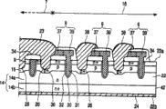
Fig. 1 shows the string that is used for the p channel mosfet 2a to 2d of being connected in series that the terminal structure according to the semiconductor device of first embodiment of the invention uses.Zener diode 8 is connected between every pair of adjacent lateral transistor.Each Zener diode is connected between the grid of another lateral transistor near the source electrode of the lateral transistor of reply mutually of active area and reply mutually.More specifically, in the embodiment in figure 1, each MOSFET has the gate electrode 4 that is connected it and the Zener diode 8 between the drain electrode 6, and the negative electrode that is provided with it is connected to gate electrode.Along this string, the source electrode 10 of the MOSFET 2a in this string is connected to the drain electrode of the next MOSFET 2b in this string, or the like.MOSFET has public body region, so and the body terminal 12 that they are shown link together.By example show four MOSFET and Zener diode right, but will recognize, according to the voltage that the device two ends are supported, can adopt the device of different numbers.In the sectional view afterwards, for the sake of clarity, in terminal structure, only show three transversal devices.
In terminal structure, an end of this string, i.e. the drain electrode of a MOSFET 2a is electrically connected to first main electrode of semiconductor device, the other end of this string, the source electrode 10 of promptly last MOSFET 2d is electrically connected to second main electrode of semiconductor device.
Have with shown in MOSFET and the Zener diode of Fig. 1 of linking together of mode, each Zener diode all is used to control the gate voltage of each MOSFET, make that MOSFET is with conducting when its threshold voltage of voltage ratio at it and relevant Zener diode two ends adds that the Zener voltage of diode is big.Be divided in the current potential that the two ends of MOSFET and diode string apply at this infall, the approximate relevant electric field that distributes has equably avoided any electric field concentration to cause premature breakdown thus in semiconductor body.
Figure 2 illustrates sectional view in conjunction with the semiconductor device of terminal structure shown in Fig. 1.
The active area 7 of this device is shown in the left side of figure, has terminal structure 16 on the right side.By example, shown active area comprises the trench-gate transistor unit.Source of making by first conduction type (in this example for n type) and drain region 9 and 14 by semiconductor body 22 (generally forming) by monocrystalline silicon in the raceway groove made of opposite second conduction type (that is, in this example, being the p type) provide and distinguish 15 and separate.Generally the gate electrode 11 that is formed by n type polysilicon is present in via in regional 9 and 15 grooves 20 that extend in the lower part in drain region 14.Gate electrode is separated by one deck gate insulation material 25 and semiconductor body.The voltage signal that imposes on gate electrode 11 with known manner when the ON state of this device is used for causing conducting channel 17 in zone 15, and the electric current that is used for this conducting channel 17 between the source of being controlled at and drain region 9 and 14 flows.
Source region 9 is by first main electrode contact of semiconductor device, and first main electrode is embodied as source electrode 23 in this example.First type surface 22a carries out this contact on the top of device main body.Shown example comprises " zanjon around " source electrode that contacts with device main body, wherein provides direct contact the between the district 15 via source region 9 etched recesses 26 can be implemented in source electrode 23 and raceway groove.This structure can make the mask number of this device preparation technology reduce, and this is because do not need the mask of the injection in patterning source region.In EP-A-0889511, disclose the example of the manufacture method of trench-gate device, thus its content has been incorporated into here as with reference to material with structure shown in Fig. 2 active area 7.
By example, Fig. 2 shows a kind of vertical device architecture, and wherein the regional 14 substrate zone 14b that are included in high conductivity (n+) go up the drain-drift region 14a by the epitaxial loayer formation of high resistivity (n-, low-doped).This substrate zone 14b can be by making with regional 14a identical conduction type (being the n type in this example), and so that a kind of vertical MOSFET to be provided, perhaps it can be made by films of opposite conductivity (being the p type in this example), so that a kind of vertical IGBT to be provided.By second main electrode, 24 contacts of semiconductor device, second main electrode 24 is called drain electrode to substrate zone 14b under the situation of MOSFET, be called positive electrode under the situation of IGBT on the end of this device main body first type surface 22b.
Terminal structure shown in Fig. 2 comprises lateral trench-gridistor unit.Each transversal device all is included in the groove 30 that wherein has gate electrode 31, and groove 30 separates by gate insulation material layer 32 and semiconductor body 22.Insulator cap 34 extends in the top of semiconductor body first type surface 22a (being restricted to the surface between the groove 26 in active area) top.When ON state (although not having conducting at this transversal device of normal work period of this device), raceway groove 35 is formed among the drain-drift region 14a, extends between the p type district 15 on the either side of groove 30.In the example shown, raceway groove 35 will be formed by p type electric charge carrier.
The drain region of the transversal device adjacent with active area is connected to source electrode 23.The source region of outmost transversal device can be by the rough surface and drain electrode 24 short circuits of formed peripheral edge 42 when cutting the semiconductor body 22 that is formed by wafer.Alternatively, zone 15 can be connected to drain electrode 24 by the additional conductive connector that extends in the semiconductor body surface.
Can see that in Fig. 2 the groove 30 of terminal structure, gate insulation material layer 32 and gate electrode 31 parts are corresponding to the structure of the groove 20 with active area, gate insulation material layer 25 and gate electrode 11.They can prepare effectively with the processing step identical with corresponding active area parts, avoid forming the additional step of these elements of terminal structure.
When continuing across terminal structure 16, the zone 9 that forms highly doped first conduction type in device source region in active area 7 is shown among Fig. 2 (with later figure).Alternatively, can shelter termination structure area to form this zone in injection period.This is to cover to inject in the embodiment of Fig. 2, and sheltering termination structure area thus will need other mask.
As shown in Figure 1, the gate electrode of lateral transistor is connected to each drain electrode by Zener diode 8 in the terminal structure.Figure 3 illustrates the enforcement of this aspect.Gate material is extended groove 30, forms extension 39.Grid extension 39 (being made by n type polysilicon in this example) becomes 37 to contact with p type polysilicon, with its formation Zener diode 8.P type polysilicon layer 37 then is electrically connected to the p type district 15 of semiconductor body by metal tape 38 on the surface of groove 26, except being used for and the relevant Zener diode of transversal device of close active area, made by source electrode 23 for its this connection.
At this material of etch-back so that it with during groove top in the active area flushes, for example by suitably sheltering the polycrystalline silicon material that deposition is filled gate groove, can provide polysilicon cambium layer 37 and extension 39.In a kind of mode, the polysilicon of deposition is in-situ doped n type, injects or spreads by the p type via suitable mask then and determine this layer 37.Alternatively, the polysilicon of deposition can be in-situ doped p type, and can shelter this layer 37 between injection of n type or diffusion period then.In another kind of mode, the polysilicon of deposition can be unadulterated, and then can by suitably shelter inject or diffusing step to its Doped n or p type to form element 37 and 39.
In another distortion, can provide extension 39 by suitable a series of depositions, doping (if this material is not in-situ doped) and etching step, and layer 37 can form by a series of these steps of separating.
This embodiment and below among those embodiment of discussing, for fear of the other special process step of needs, in terminal structure, can form metal tape 38 (with the 38a in Fig. 6) with the processing step identical with the source electrode.
Shown in Fig. 2,3 and 6, the raceway groove between the source region 9 adjacent with top first type surface 22a provides in the district 15 can comprise p type zone 36, and it provides the district 15 doping De Genggao than raceway groove.These zones can form by injecting via the window of appropriate mask.These zones are used to be given in raceway groove in known manner provides good contact between district 15 and the source electrode 23.They also can be included in the terminal structure in the embodiments of figure 3, to strengthen the contact between zone 15 and the metal tape 38.Raceway groove in zone 36 also comparable active areas and/or the terminal structure provides district 15 to extend deeplyer, to reduce near the electric field in adjacent trenches bottom.
Can allow polycrystal layer 37 and the metal tape 38 necessary spacings zone that terminal structure is shared to reduce to minimum by in the major part of structure, having contiguous groove pitch and only increasing.For example, be schematically shown as Fig. 4, Zener diode 8 can be provided with towards a turning of semiconductor body, and is adjacent with the peripheral edge 42 of semiconductor body.The parts of the semiconductor device of the element of describing in the coverage diagram 4 are not shown for illustrative purposes.In the example of Fig. 4, the groove 30 of five band shape geometries is around active area 7 in terminal structure 16.The groove of active area 7 also can have band shape geometry.To recognize, can use other geometry for active area, for example, as (close-packed) hex shape of square or solid matter.
The optional structure of Fig. 1 is shown among Fig. 5.In this example, each Zener diode 8 all is connected between the grid of the adjacent lateral transistors of tackling mutually in this string.That is, the negative electrode of first Zener diode is connected to the grid of transistor 2d, and its anode is connected to the grid of transistor 2c, or the like.Another diode has the negative electrode of the grid that is connected to transistor 2a and is connected to the anode of first main electrode of semiconductor device.The grid of transistor 2d is connected to second main electrode of semiconductor device.
In the structure of Fig. 5, the string of transistor and diode can be supported 4 times maximum voltage drop of the Zener voltage of diode.
Figure 6 illustrates sectional view in conjunction with the semiconductor device of terminal structure shown in Fig. 5.The cross section is to pass the zone that Zener diode is provided.For example, the cross section of the position in the remainder of terminal structure can be identical with above-mentioned Fig. 2.In the mode similar to the embodiment of Fig. 3, metal tape 38 contacts with n type polysilicon layer 37.Compare with Fig. 3, the metal tape 38 of Fig. 6 also contact with gate electrode extension 39 near the adjacent lateral transistors on active area 7 one sides, and insulate with the p type district 15 of semiconductor body.Be used for being connected together with the polyphone of Zener diode at this metal tape 38 (rather than continue n type polysilicon layer 37 to contact the grid extension 39 of adjacent transistor, will form Zener diode back-to-back as this).
In the embodiment of Fig. 6, provide another metal tape 38a, with the gate electrode that is provided at the outermost transversal device and the electrical connection between its source region.Technology in this source region by cut edge 42 is followed and drain region short circuit (or other Elecrical connector can provide this connection).
Fig. 7 is the plane graph according to the corner part of the semiconductor body of Fig. 6 embodiment, shows the structure of the Zener diode in the terminal structure 16.In this example, the groove of four band shape geometries is around the active area 7 of device in terminal structure.As Fig. 4,, the parts of the semiconductor device of 7 elements depicted of coverage diagram are not shown for illustrative purpose.
In the general example of device shown in Figure 2, the spacing of transversal device is 2.4 microns in terminal structure 16, and groove width is 0.5 micron.Gate insulation layer 25 is silicon dioxide layers of 40nm, and n type zone 14a has 1 * 10 16Individual phosphorus or the every cm of arsenic atom 3Doping level, p type zone has 1 * 10 17The every cm of boron atom 3Doping level.Gate electrode is by having 1 * 10 20The every cm of individual phosphorus atoms 3The n type polysilicon of doping level form.
In the Zener diode shown in Fig. 3 and 6, the p type doping level of polysilicon layer 37 generally can be 1 * 10 19The every cm of individual boron atom 3Therefore, in this example, polysilicon forms element 37 and 39, and doped p type then can be in 1 * 10 of increase to this level equably at first 20The every cm of individual phosphorus atoms 3The n type dopant of concentration during shelter this layer 37 so that in element 39 overdoping p type dopant.To recognize that the doping level that can change element 37 and 39 is adjusted to a certain degree with the Zener voltage with resulting diode.
For the Zener diode 8 shown in Fig. 3 and 6 is provided, the spacing of transversal device can be increased to for example about 15 microns partly.
In example of structure shown in Figure 3, have the above parameter that provides, will have the threshold voltage of about 2.3V with peripheral edge 42 adjacent transistors of this device, and Zener diode is about 7.5V.Therefore being combined in about 9.8V (or summary at this more than value) and will beginning conducting of transistor and diode, and this voltage is sent to the source electrode of adjacent lateral device.Therefore this will have at its source electrode and the reverse bias between the regional 14a, make its threshold voltage be increased to about 3.8V.Therefore the string of device and diode transversely, the voltage of supporting at the two ends of transistor seconds and diode pair is about 11.3V, or the like.Utilize the string of 4 pairs of devices, terminal structure can tolerate about 45V.When the spacing of transversal device is 2.4 microns, provide terminal structure only to need 9.6 microns.
In the embodiment of Fig. 5, the voltage drop at the two ends of the string of transversal device and Zener diode equal Zener diode Zener voltage and.For example, use parameter described above, the string of four Zener diodes will make voltage drop to 30V.
Trench-gate device in the active area of above description embodiment has the source configuration that zanjon centers on.To recognize that the present invention may be used on wherein instead sheltering on the structure of the injection that forms the source region equally.Under the sort of situation, shelter this injection, make that separating the source region adjacent with each groove contacts p type zone 15 to allow the metal tape 38 in the terminal structure at the top of semiconductor body first type surface 22a place.
The present invention may be used on plane gated device and trench-gate device.By explanation the cross section of using plane gated device of the present invention has been shown in Fig. 8 and 9.These figure are similar with in 3 those to Fig. 2 respectively, and as Fig. 2 and 3, show to have the embodiment that source electrode that zanjon centers on contacts in the active area that is provided with and the Zener diode in the terminal structure according to Fig. 1.As shown in Figure 9, plane gate electrode 31 ' (being made by n type polysilicon in this example) extended above semiconductor body 22 and formed and the Zener diode 8 of each p type polysilicon layer 37 adjacency.
Though more than described the present invention has MOSFET in active area device, it is evident that, for example, but in the scope of other device such as IGBT, thyristor or rectifier use side minor structure also.Device at active area comprises that the position component application that forms with the processing step identical with the parts of terminal structure is especially favourable.
To recognize, in above example, mention specific conduction type, for opposite conduction type it within the scope of the present invention, with reference to replaced the n type by the p type, vice versa.In the example of describing in the drawings, active area is the n channel device, and wherein zone 9 and 14 is made by n type conductivity, and zone 15 is made by the p type, and is caused the raceway groove 17 of electron inversion in zone 15 by gate electrode 11.By using the dopant of films of opposite conductivity, replacing these devices is p channel devices.In this case, zone 9 and 14 is made by p type conductivity, and zone 15 is made by the n type, and causes hole inversion channel 17 by gate electrode 11 in zone 15.In addition, in this embodiment, if the transversal device conducting, the raceway groove 35 that causes substantially in terminal structure will be the electron inversion channel among the 14a of p type zone.
From having read the disclosure, other distortion and modification will be conspicuous for those skilled in the art.This distortion and revise can comprise equivalent and known in the art and can use replacement or other parts except the parts of having described at this.
Though claim is expressed as the concrete combination of parts in this application, but should be understood that, scope disclosed by the invention also comprises the parts of arbitrary novelty or this clearly or implicitly openly combination or its all summary of arbitrary novelty of parts, no matter its whether relate to have arbitrary claim in desired identical invention or whether reduced and identical some or all of technical problem to be solved by this invention.
Also can in single embodiment, make up and be provided at the parts of describing in the context of independent embodiment.On the contrary, for the sake of brevity, the various parts of describing in the context of single embodiment also provide separably or with any suitable sub-portfolio.The applicant proposes to note thus, during any other application of implementing the application or deriving thus, new claim can be expressed as the combination of this parts and/or these parts.

Claims (11)

1. semiconductor device with semiconductor body (22), this semiconductor body (22) includes source region (7) and centers on the terminal structure (16) of active area, this terminal structure comprises that a plurality of lateral transistor devices (2a to 2d) and the peripheral edge from active area towards semiconductor body (42) that are connected in series extend, has Zener diode (8), the gate electrode (4) that this Zener diode one of is connected in the transversal device is used to control its gate voltage, so that the voltage difference between active area and the peripheral edge is distributed in the two ends of transversal device and Zener diode.
2. semiconductor device as claimed in claim 1, wherein Zener diode (8) is connected between every pair of adjacent lateral transistor (2a to 2d).
3. semiconductor device as claimed in claim 2, wherein each Zener diode (8) all is connected between the gate electrode (4) near the source electrode (10) of the lateral transistor of reply mutually of active area (7) and another lateral transistor of tackling mutually.
4. semiconductor device as claimed in claim 2, wherein each Zener diode (8) all is connected between the gate electrode (4) of the lateral transistor of tackling mutually.
5 semiconductor device as claimed in claim 1, wherein each transversal device (2a to 2d) all comprises the gate electrode (31) by the insulation of gate insulation material layer (32) and semiconductor body (22), the gate electrode of this transversal device and gate insulation material layer respectively with the insulated electrode (11) of device in active area (7) and each identical technology formation of material layer (25) that insulated electrode is insulated.
6. semiconductor device as claimed in claim 5, wherein active area (7) comprises trench-gate semiconductor device, and the lateral transistor of terminal structure (16) is the trench-gate transistor.
7. as the semiconductor device of claim 5 or claim 6, wherein each transversal device (2a to 2d) all is included in the groove (30) that wherein has gate electrode (31), and the groove of this transversal device forms with each processing step identical with the gate trench (20) of device in the active area (7).
8. semiconductor device as claimed in claim 5, wherein active area (7) comprises plane gate semiconductor device, and the lateral transistor of this terminal structure (16) is plane gridistor.
9. as each semiconductor device in claim 1 to 6 and 8, wherein this transversal device (2a to 2d) comprises the zone (15) of first conduction type, top of zone (14a) below second films of opposite conductivity, the zone of this first conduction type (15), and wherein active area (7) comprises the device in the zone (15) with first conduction type, and this zone (15) form with the processing step identical with first conductivity type regions of this transversal device.
10. as each semiconductor device in the claim 5,6 and 8, wherein the gate electrode of this transversal device (31) is formed by polysilicon, and this Zener diode (8) is by forming with the polysilicon that processing step was deposited identical with gate electrode.
11. formation method with semiconductor device of semiconductor body (22), this semiconductor body (22) includes source region (7) and centers on the terminal structure (16) of active area, this terminal structure comprises that a plurality of lateral transistor devices (2a to 2d) and the peripheral edge from active area towards semiconductor body (42) that are connected in series extend, has Zener diode (8), the gate electrode (4) that this Zener diode one of is connected in the transversal device is used to control its gate voltage, so that the voltage difference between active area and the peripheral edge is distributed in the two ends of transversal device and Zener diode, wherein the gate electrode of transversal device (31) is formed by polysilicon, and this method comprises that formation is by the Zener diode made from the polysilicon that processing step was deposited identical with gate electrode (8).
12. method as claim 11, wherein each transversal device (2a to 2d) all is included in the groove (30) that wherein has gate electrode (31), and this method comprises the groove that forms this transversal device with each processing step identical with the gate trench (20) of device in the active area (7).
CNB2004800148427A 2003-05-31 2004-05-21 Termination structures for semiconductor devices and the manufacture thereof Expired - Fee Related CN100442537C (en)

Applications Claiming Priority (2)

Application Number Priority Date Filing Date Title
GBGB0312514.3A GB0312514D0 (en) 2003-05-31 2003-05-31 Termination structures for semiconductor devices and the manufacture thereof
GB0312514.3 2003-05-31

Publications (2)

Publication Number Publication Date
CN1799144A CN1799144A (en) 2006-07-05
CN100442537C true CN100442537C (en) 2008-12-10

Family

ID=9959102

Family Applications (1)

Application Number Title Priority Date Filing Date
CNB2004800148427A Expired - Fee Related CN100442537C (en) 2003-05-31 2004-05-21 Termination structures for semiconductor devices and the manufacture thereof

Country Status (7)

Country Link
US (1) US20080116520A1 (en)
EP (1) EP1634337A1 (en)
JP (1) JP2006526287A (en)
KR (1) KR20060036393A (en)
CN (1) CN100442537C (en)
GB (1) GB0312514D0 (en)
WO (1) WO2004107449A1 (en)

Families Citing this family (12)

* Cited by examiner, † Cited by third party
Publication number Priority date Publication date Assignee Title
JP4913336B2 (en) * 2004-09-28 2012-04-11 ルネサスエレクトロニクス株式会社 Semiconductor device
US8110868B2 (en) 2005-07-27 2012-02-07 Infineon Technologies Austria Ag Power semiconductor component with a low on-state resistance
EP2261992A3 (en) * 2005-07-27 2011-02-23 Infineon Technologies Austria AG Semiconductor component with a drift region and with a drift control region
US8461648B2 (en) 2005-07-27 2013-06-11 Infineon Technologies Austria Ag Semiconductor component with a drift region and a drift control region
DE102005061210B4 (en) * 2005-12-21 2009-05-14 Infineon Technologies Austria Ag Semiconductor device having a front and a back pn junction and associated manufacturing method
US7564096B2 (en) 2007-02-09 2009-07-21 Fairchild Semiconductor Corporation Scalable power field effect transistor with improved heavy body structure and method of manufacture
JP2012064849A (en) * 2010-09-17 2012-03-29 Toshiba Corp Semiconductor device
CN102569388B (en) * 2010-12-23 2014-09-10 无锡华润上华半导体有限公司 Semiconductor device and manufacturing method thereof
US8598655B1 (en) * 2012-08-03 2013-12-03 Infineon Technologies Dresden Gmbh Semiconductor device and method for manufacturing a semiconductor device
CN106024866B (en) * 2016-07-25 2019-03-29 电子科技大学 A kind of groove-shaped terminal structure of power semiconductor
KR102281493B1 (en) * 2017-02-03 2021-07-23 매그나칩 반도체 유한회사 Power semiconductor device and manufacturing method thereof
KR102463902B1 (en) * 2017-12-08 2022-11-08 한국전자통신연구원 MOS structure thyristor device built in diode

Citations (4)

* Cited by examiner, † Cited by third party
Publication number Priority date Publication date Assignee Title
US5557127A (en) * 1995-03-23 1996-09-17 International Rectifier Corporation Termination structure for mosgated device with reduced mask count and process for its manufacture
US6204097B1 (en) * 1999-03-01 2001-03-20 Semiconductor Components Industries, Llc Semiconductor device and method of manufacture
US6407413B1 (en) * 2000-02-01 2002-06-18 Mitsubishi Denki Kabushiki Kaisha Semiconductor device with guard ring and Zener diode layer thereover
US6462376B1 (en) * 1999-01-11 2002-10-08 Fraunhofer-Gesellschaft Zur Foerderung Der Angewandten Forschung E.V. Power MOS element and method for producing the same

Family Cites Families (2)

* Cited by examiner, † Cited by third party
Publication number Priority date Publication date Assignee Title
JP2689703B2 (en) 1989-08-03 1997-12-10 富士電機株式会社 MOS type semiconductor device
JP3191747B2 (en) * 1997-11-13 2001-07-23 富士電機株式会社 MOS type semiconductor device

Patent Citations (4)

* Cited by examiner, † Cited by third party
Publication number Priority date Publication date Assignee Title
US5557127A (en) * 1995-03-23 1996-09-17 International Rectifier Corporation Termination structure for mosgated device with reduced mask count and process for its manufacture
US6462376B1 (en) * 1999-01-11 2002-10-08 Fraunhofer-Gesellschaft Zur Foerderung Der Angewandten Forschung E.V. Power MOS element and method for producing the same
US6204097B1 (en) * 1999-03-01 2001-03-20 Semiconductor Components Industries, Llc Semiconductor device and method of manufacture
US6407413B1 (en) * 2000-02-01 2002-06-18 Mitsubishi Denki Kabushiki Kaisha Semiconductor device with guard ring and Zener diode layer thereover

Also Published As

Publication number Publication date
GB0312514D0 (en) 2003-07-09
EP1634337A1 (en) 2006-03-15
WO2004107449A1 (en) 2004-12-09
US20080116520A1 (en) 2008-05-22
KR20060036393A (en) 2006-04-28
JP2006526287A (en) 2006-11-16
CN1799144A (en) 2006-07-05

Similar Documents

Publication Publication Date Title
US4376286A (en) High power MOSFET with low on-resistance and high breakdown voltage
US4642666A (en) High power MOSFET with low on-resistance and high breakdown voltage
US4959699A (en) High power MOSFET with low on-resistance and high breakdown voltage
JP2968222B2 (en) Semiconductor device and method for preparing silicon wafer
US8872264B2 (en) Semiconductor device having a floating semiconductor zone
US7560787B2 (en) Trench field plate termination for power devices
US6362505B1 (en) MOS field-effect transistor with auxiliary electrode
EP1033759B1 (en) MOS-gated device having a buried gate and process for forming same
US8344448B2 (en) Semiconductor device having an edge termination structure and method of manufacture thereof
EP4143889A1 (en) Trenched power device with segmented trench and shielding
CN1468449A (en) Trench dmos transistor with embedded trench schottky rectifier
JPH0336311B2 (en)
KR20040078149A (en) Cellular mosfet devices and their manufacture
US9929259B2 (en) Semiconductor device and manufacturing method for semiconductor device
CN100442537C (en) Termination structures for semiconductor devices and the manufacture thereof
JPH07120799B2 (en) Semiconductor device
KR19990029884A (en) Semiconductor devices
KR101550798B1 (en) Power semiconductor device having structure for preventing latch-up and method of manufacture thereof
US20220130997A1 (en) Gate trench power semiconductor devices having improved deep shield connection patterns
US11094691B2 (en) Semiconductor device
US8222689B2 (en) High-voltage metal oxide semiconductor device and fabrication method thereof
GB2080616A (en) Power semiconductor devices
KR100300674B1 (en) Slope Concentration Epitaxial Board of Semiconductor Device with Resurf Diffusion
CN116741828A (en) Trench gate transistor assembly
JPH04355966A (en) Electrostatic induction type semiconductor element and manufacture thereof

Legal Events

Date Code Title Description
C06 Publication
PB01 Publication
C10 Entry into substantive examination
SE01 Entry into force of request for substantive examination
ASS Succession or assignment of patent right

Owner name: NXP CO., LTD.

Free format text: FORMER OWNER: KONINKLIJKE PHILIPS ELECTRONICS N.V.

Effective date: 20071012

C41 Transfer of patent application or patent right or utility model
TA01 Transfer of patent application right

Effective date of registration: 20071012

Address after: Holland Ian Deho Finn

Applicant after: Koninkl Philips Electronics NV

Address before: Holland Ian Deho Finn

Applicant before: Koninklijke Philips Electronics N.V.

C14 Grant of patent or utility model
GR01 Patent grant
C17 Cessation of patent right
CF01 Termination of patent right due to non-payment of annual fee

Granted publication date: 20081210

Termination date: 20130521