CN100421226C - Methods of forming a transistor with an integrated metal silicide gate electrode - Google Patents
Methods of forming a transistor with an integrated metal silicide gate electrode Download PDFInfo
- Publication number
- CN100421226C CN100421226C CNB2004800304590A CN200480030459A CN100421226C CN 100421226 C CN100421226 C CN 100421226C CN B2004800304590 A CNB2004800304590 A CN B2004800304590A CN 200480030459 A CN200480030459 A CN 200480030459A CN 100421226 C CN100421226 C CN 100421226C
- Authority
- CN
- China
- Prior art keywords
- layer
- groove
- silicon
- isolation
- metal silicide
- Prior art date
- Legal status (The legal status is an assumption and is not a legal conclusion. Google has not performed a legal analysis and makes no representation as to the accuracy of the status listed.)
- Active
Links
- 229910052751 metal Inorganic materials 0.000 title claims abstract description 81
- 239000002184 metal Substances 0.000 title claims abstract description 81
- 229910021332 silicide Inorganic materials 0.000 title claims abstract description 64
- FVBUAEGBCNSCDD-UHFFFAOYSA-N silicide(4-) Chemical compound [Si-4] FVBUAEGBCNSCDD-UHFFFAOYSA-N 0.000 title claims abstract description 63
- 238000000034 method Methods 0.000 title claims abstract description 41
- 229910052710 silicon Inorganic materials 0.000 claims abstract description 77
- 239000010703 silicon Substances 0.000 claims abstract description 77
- 238000002955 isolation Methods 0.000 claims abstract description 73
- 239000004065 semiconductor Substances 0.000 claims abstract description 50
- 125000006850 spacer group Chemical group 0.000 claims abstract description 13
- XUIMIQQOPSSXEZ-UHFFFAOYSA-N Silicon Chemical compound [Si] XUIMIQQOPSSXEZ-UHFFFAOYSA-N 0.000 claims description 79
- 239000010941 cobalt Substances 0.000 claims description 42
- 229910017052 cobalt Inorganic materials 0.000 claims description 42
- GUTLYIVDDKVIGB-UHFFFAOYSA-N cobalt atom Chemical compound [Co] GUTLYIVDDKVIGB-UHFFFAOYSA-N 0.000 claims description 41
- 229910021420 polycrystalline silicon Inorganic materials 0.000 claims description 41
- 229920005591 polysilicon Polymers 0.000 claims description 38
- 239000000463 material Substances 0.000 claims description 34
- 239000000758 substrate Substances 0.000 claims description 33
- 239000010936 titanium Substances 0.000 claims description 30
- RTAQQCXQSZGOHL-UHFFFAOYSA-N Titanium Chemical compound [Ti] RTAQQCXQSZGOHL-UHFFFAOYSA-N 0.000 claims description 28
- 229910052719 titanium Inorganic materials 0.000 claims description 28
- 238000005530 etching Methods 0.000 claims description 24
- 229910019001 CoSi Inorganic materials 0.000 claims description 23
- 230000015572 biosynthetic process Effects 0.000 claims description 22
- 238000000137 annealing Methods 0.000 claims description 17
- 238000000151 deposition Methods 0.000 claims description 15
- 238000006243 chemical reaction Methods 0.000 claims description 14
- 239000011248 coating agent Substances 0.000 claims description 12
- 238000000576 coating method Methods 0.000 claims description 12
- PXHVJJICTQNCMI-UHFFFAOYSA-N Nickel Chemical compound [Ni] PXHVJJICTQNCMI-UHFFFAOYSA-N 0.000 claims description 10
- 239000000428 dust Substances 0.000 claims description 9
- 238000000059 patterning Methods 0.000 claims description 8
- 239000012535 impurity Substances 0.000 claims description 7
- 229920002120 photoresistant polymer Polymers 0.000 claims description 7
- NRTOMJZYCJJWKI-UHFFFAOYSA-N Titanium nitride Chemical compound [Ti]#N NRTOMJZYCJJWKI-UHFFFAOYSA-N 0.000 claims description 6
- 239000000203 mixture Substances 0.000 claims description 6
- 239000002210 silicon-based material Substances 0.000 claims description 6
- 229910052759 nickel Inorganic materials 0.000 claims description 5
- 238000003860 storage Methods 0.000 claims description 4
- 230000005669 field effect Effects 0.000 claims description 2
- 150000001875 compounds Chemical class 0.000 claims 2
- 239000008187 granular material Substances 0.000 claims 2
- 101100373011 Drosophila melanogaster wapl gene Proteins 0.000 claims 1
- 210000004483 pasc Anatomy 0.000 claims 1
- 238000007669 thermal treatment Methods 0.000 claims 1
- 238000004519 manufacturing process Methods 0.000 abstract description 10
- 235000013495 cobalt Nutrition 0.000 description 30
- VYPSYNLAJGMNEJ-UHFFFAOYSA-N Silicium dioxide Chemical compound O=[Si]=O VYPSYNLAJGMNEJ-UHFFFAOYSA-N 0.000 description 26
- 229910052581 Si3N4 Inorganic materials 0.000 description 18
- HQVNEWCFYHHQES-UHFFFAOYSA-N silicon nitride Chemical compound N12[Si]34N5[Si]62N3[Si]51N64 HQVNEWCFYHHQES-UHFFFAOYSA-N 0.000 description 18
- 239000000377 silicon dioxide Substances 0.000 description 13
- 235000012239 silicon dioxide Nutrition 0.000 description 13
- 230000008021 deposition Effects 0.000 description 7
- 239000002245 particle Substances 0.000 description 7
- 229910018999 CoSi2 Inorganic materials 0.000 description 5
- 239000011435 rock Substances 0.000 description 4
- 239000003153 chemical reaction reagent Substances 0.000 description 3
- -1 hydrochloric acid peroxide Chemical class 0.000 description 3
- 150000004767 nitrides Chemical class 0.000 description 3
- 230000000717 retained effect Effects 0.000 description 3
- 229910021341 titanium silicide Inorganic materials 0.000 description 3
- WQJQOUPTWCFRMM-UHFFFAOYSA-N tungsten disilicide Chemical compound [Si]#[W]#[Si] WQJQOUPTWCFRMM-UHFFFAOYSA-N 0.000 description 3
- 229910021342 tungsten silicide Inorganic materials 0.000 description 3
- 235000011114 ammonium hydroxide Nutrition 0.000 description 2
- 238000010586 diagram Methods 0.000 description 2
- 238000011049 filling Methods 0.000 description 2
- 238000010438 heat treatment Methods 0.000 description 2
- VEXZGXHMUGYJMC-UHFFFAOYSA-N hydrochloric acid Substances Cl VEXZGXHMUGYJMC-UHFFFAOYSA-N 0.000 description 2
- 238000002347 injection Methods 0.000 description 2
- 239000007924 injection Substances 0.000 description 2
- 239000012212 insulator Substances 0.000 description 2
- 238000001465 metallisation Methods 0.000 description 2
- 150000002978 peroxides Chemical class 0.000 description 2
- 229910052594 sapphire Inorganic materials 0.000 description 2
- 239000010980 sapphire Substances 0.000 description 2
- 230000010415 tropism Effects 0.000 description 2
- 238000001039 wet etching Methods 0.000 description 2
- 229910001218 Gallium arsenide Inorganic materials 0.000 description 1
- 229910000577 Silicon-germanium Inorganic materials 0.000 description 1
- 150000001868 cobalt Chemical class 0.000 description 1
- 239000004020 conductor Substances 0.000 description 1
- 239000003989 dielectric material Substances 0.000 description 1
- 229910052732 germanium Inorganic materials 0.000 description 1
- GNPVGFCGXDBREM-UHFFFAOYSA-N germanium atom Chemical compound [Ge] GNPVGFCGXDBREM-UHFFFAOYSA-N 0.000 description 1
- 238000003475 lamination Methods 0.000 description 1
- 239000002243 precursor Substances 0.000 description 1
- 239000000243 solution Substances 0.000 description 1
Images


Classifications
-
- H—ELECTRICITY
- H01—ELECTRIC ELEMENTS
- H01L—SEMICONDUCTOR DEVICES NOT COVERED BY CLASS H10
- H01L21/00—Processes or apparatus adapted for the manufacture or treatment of semiconductor or solid state devices or of parts thereof
- H01L21/02—Manufacture or treatment of semiconductor devices or of parts thereof
- H01L21/04—Manufacture or treatment of semiconductor devices or of parts thereof the devices having at least one potential-jump barrier or surface barrier, e.g. PN junction, depletion layer or carrier concentration layer
- H01L21/18—Manufacture or treatment of semiconductor devices or of parts thereof the devices having at least one potential-jump barrier or surface barrier, e.g. PN junction, depletion layer or carrier concentration layer the devices having semiconductor bodies comprising elements of Group IV of the Periodic System or AIIIBV compounds with or without impurities, e.g. doping materials
- H01L21/28—Manufacture of electrodes on semiconductor bodies using processes or apparatus not provided for in groups H01L21/20 - H01L21/268
- H01L21/28008—Making conductor-insulator-semiconductor electrodes
- H01L21/28017—Making conductor-insulator-semiconductor electrodes the insulator being formed after the semiconductor body, the semiconductor being silicon
- H01L21/28026—Making conductor-insulator-semiconductor electrodes the insulator being formed after the semiconductor body, the semiconductor being silicon characterised by the conductor
- H01L21/28035—Making conductor-insulator-semiconductor electrodes the insulator being formed after the semiconductor body, the semiconductor being silicon characterised by the conductor the final conductor layer next to the insulator being silicon, e.g. polysilicon, with or without impurities
- H01L21/28044—Making conductor-insulator-semiconductor electrodes the insulator being formed after the semiconductor body, the semiconductor being silicon characterised by the conductor the final conductor layer next to the insulator being silicon, e.g. polysilicon, with or without impurities the conductor comprising at least another non-silicon conductive layer
- H01L21/28052—Making conductor-insulator-semiconductor electrodes the insulator being formed after the semiconductor body, the semiconductor being silicon characterised by the conductor the final conductor layer next to the insulator being silicon, e.g. polysilicon, with or without impurities the conductor comprising at least another non-silicon conductive layer the conductor comprising a silicide layer formed by the silicidation reaction of silicon with a metal layer
-
- H—ELECTRICITY
- H01—ELECTRIC ELEMENTS
- H01L—SEMICONDUCTOR DEVICES NOT COVERED BY CLASS H10
- H01L29/00—Semiconductor devices adapted for rectifying, amplifying, oscillating or switching, or capacitors or resistors with at least one potential-jump barrier or surface barrier, e.g. PN junction depletion layer or carrier concentration layer; Details of semiconductor bodies or of electrodes thereof ; Multistep manufacturing processes therefor
- H01L29/66—Types of semiconductor device ; Multistep manufacturing processes therefor
- H01L29/66007—Multistep manufacturing processes
- H01L29/66075—Multistep manufacturing processes of devices having semiconductor bodies comprising group 14 or group 13/15 materials
- H01L29/66227—Multistep manufacturing processes of devices having semiconductor bodies comprising group 14 or group 13/15 materials the devices being controllable only by the electric current supplied or the electric potential applied, to an electrode which does not carry the current to be rectified, amplified or switched, e.g. three-terminal devices
- H01L29/66409—Unipolar field-effect transistors
- H01L29/66477—Unipolar field-effect transistors with an insulated gate, i.e. MISFET
- H01L29/66568—Lateral single gate silicon transistors
- H01L29/66575—Lateral single gate silicon transistors where the source and drain or source and drain extensions are self-aligned to the sides of the gate
- H01L29/66583—Lateral single gate silicon transistors where the source and drain or source and drain extensions are self-aligned to the sides of the gate with initial gate mask or masking layer complementary to the prospective gate location, e.g. with dummy source and drain contacts
-
- H—ELECTRICITY
- H01—ELECTRIC ELEMENTS
- H01L—SEMICONDUCTOR DEVICES NOT COVERED BY CLASS H10
- H01L29/00—Semiconductor devices adapted for rectifying, amplifying, oscillating or switching, or capacitors or resistors with at least one potential-jump barrier or surface barrier, e.g. PN junction depletion layer or carrier concentration layer; Details of semiconductor bodies or of electrodes thereof ; Multistep manufacturing processes therefor
- H01L29/40—Electrodes ; Multistep manufacturing processes therefor
- H01L29/43—Electrodes ; Multistep manufacturing processes therefor characterised by the materials of which they are formed
- H01L29/49—Metal-insulator-semiconductor electrodes, e.g. gates of MOSFET
- H01L29/4916—Metal-insulator-semiconductor electrodes, e.g. gates of MOSFET the conductor material next to the insulator being a silicon layer, e.g. polysilicon doped with boron, phosphorus or nitrogen
- H01L29/4925—Metal-insulator-semiconductor electrodes, e.g. gates of MOSFET the conductor material next to the insulator being a silicon layer, e.g. polysilicon doped with boron, phosphorus or nitrogen with a multiple layer structure, e.g. several silicon layers with different crystal structure or grain arrangement
- H01L29/4933—Metal-insulator-semiconductor electrodes, e.g. gates of MOSFET the conductor material next to the insulator being a silicon layer, e.g. polysilicon doped with boron, phosphorus or nitrogen with a multiple layer structure, e.g. several silicon layers with different crystal structure or grain arrangement with a silicide layer contacting the silicon layer, e.g. Polycide gate
Abstract
Methods of forming a transistor having integrated metal silicide transistor gate electrode an a semiconductor assembly are described. The transistor gate is partially fabricated by reacting the metal with epitaxial silicon while residing in a trench to form metal silicide. A transistor gate isolation capping layer is formed in the trench and an the metal silicide. Optional trench spacers can be added to reduce the critical dimension restraints of a given fabrication process and thus form a transistor having smaller feature sizes than the critical dimension.
Description
Priority
The application require to enjoy submit on August 15th, 2003, series number is the priority of 10/641851 U.S. Patent application.
Technical field
The present invention relates to form production process of semiconductor device.This invention relates in particular to the transistorized method that is used for the integrated metal silicide gate electrode of having of semiconductor device of making.
Background technology
At semiconductor device for example in the dynamic random access memory (DRAM), transistor gate mainly for example make by the conductor layer of polysilicon and stack by titanium silicide or tungsten silicide.Yet tungsten silicide and titanium silicide belong to the larger particles material, therefore cause the coarse of silicide/silicon, and this has increased the impedance of transistor gate stack.
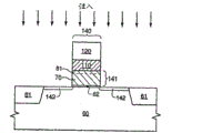
Nearest semiconductor making method is being developed metal silicide for example cobalt silicide or the nickle silicide of introducing other type always, and they are compared with titanium silicide or tungsten silicide material, are the particle materials with smaller.Yet,, therefore may be difficult to these metal silicides are incorporated in the current manufacturing process because the metal silicide of etching smaller particle size has difficulties.For example, in Fig. 1-5 of prior art, a kind of technology has been shown.
As shown in Figure 1, on silicon substrate 10, be formed with in order to make up the multilayer material of transistor gate stack.After forming first grid oxide 11, then form polysilicon layer 12, titanium or titanium nitride (Ti/TiN) layer 13, cobalt layer 14, silicon layer 15, nitride layer 16 and final pattern photoresist 17.
As shown in Figure 2, implement a kind of etching, by stopping, to begin to form transistor gate stack to nitride 16, silicon 15 patternings and at cobalt layer 14.Silicon 15 is forced to and 14 reaction of cobalt layer, and they contact with each other there, form cobalt silicide 30, as shown in Figure 3.Because this reaction also can isotropically produce (on vertical and horizontal both direction), so cobalt silicide 30 expands to outside the scope (being limited by nitride 16) of original gate stack pattern.As shown in Figure 4 and Figure 5,, need two additional etchings for finishing transistor gate stack, the wet cobalt material of removing the gate stack outside of carving, an etching is to Ti/TiN layer 13, polysilicon 12 and gate oxide 11 patternings.Yet cobalt silicide 30 can not be subjected to the current influence that is used to finish the etching chemistry reagent of transistor gate stack, thereby has increased the width of gate stack.
Therefore, top method needs some etching steps, it has increased the critical dimension of device feature size, and increases the impedance of transistor gate stack probably, because this method needs enough silicon 15 to guarantee that cobalts all during reactions steps is converted to cobalt silicide.This probably can cause a spot of silicon of residue in gate stack, thereby has increased any impedance that contacts with this lamination.
At present, in semiconductor is made, need a kind of method under the situation of the characteristic size that does not increase contact impedance or this device, to form the metal silicide portion of transistor gate, this also allows the integrated transistor gate cap, this cap rock can be used for forming n raceway groove and two kinds of transistorized grids of p raceway groove in semiconductor device, to of the present invention open, those of ordinary skills obviously can solve this needs by following.
Summary of the invention
Illustrative embodiments of the present invention comprises by for example forming the transistor with integrated metal silicide transistor gate at semiconductor device on the silicon substrate and form transistorized method in semiconductor device.This transistor gate is partly made to form metal silicide by the reaction of metal and epitaxial silicon is stayed in the groove simultaneously.Preferred metal silicide is cobalt silicide or nickle silicide.In this groove and on this metal silicide, form the transistor gate isolation cap rock.Can add optional trench spacers, reducing the critical dimension restriction of given manufacturing process, and thereby form transistor with characteristic size littler than critical dimension.
Description of drawings
Fig. 1-the 5th explains in the prior art figure of semiconductor making method that comprises the transistor gate stack of cobalt silicide in order to formation.
Fig. 6 is the sectional view of Semiconductor substrate part, and it illustrates the example that manufacturing of the present invention has a transistorized method of metal silicide gate and integrated isolation cap.
Fig. 7 is the sectional view of Semiconductor substrate part, and it illustrates the commitment of making according to the semiconductor of first embodiment of the invention, in this stage substrate is handled, and forms channel separating zone in conductivity p type silicon substrate, and forms oxide skin(coating) on it.On this oxide skin(coating), form polysilicon layer, and on polysilicon layer, form trench isolation.On trench isolation, form the photoresist of patterning then.
Fig. 8 be after Fig. 7 in trench isolation etched trench, then grow the subsequent cross-sectional view of epitaxial silicon in the bottom of groove.
Fig. 9 be after Fig. 8 depositing metal layers on the semiconductor device and on metal level the subsequent cross-sectional view of depositing conducting layer.
Figure 10 be after Fig. 9, take annealing steps so that metal level and below epitaxial silicon reaction to form the subsequent cross-sectional view of metal silicide.
Figure 11 removes any unreacted metal layer and conductive layer and takes optional second annealing steps so that the subsequent cross-sectional view that the formation of metal silicide is proceeded after Figure 10.
Figure 12 is the subsequent cross-sectional view that deposits isolation cap after Figure 11 for transistor gate.
Figure 13 carries out side direction partly the subsequent cross-sectional view of selective etch to remove isolation cap after Figure 12.
Figure 14 carries out selective etch to form transistor gate stack and to carry out the autoregistration injection to form the subsequent cross-sectional view in transistorized lightly doped source/drain region thereafter to isolation cap after Figure 13.
Figure 15 is the subsequent cross-sectional view that forms transistor gate sidewall isolation spacer and inject source/drain region subsequently after Figure 14.
Figure 16 is the plan view from above of Figure 15, and it illustrates as the complete transistor first embodiment of the invention manufacturing, that have metal silicide gate and be superimposed with integrated transistor isolation cap.
Figure 17 according to second embodiment of the invention, after Fig. 7 in trench isolation etched trench and the surface of trench isolation, along the madial wall of groove and below the surface of expose portion of polysilicon layer on the sectional view of deposition one deck spacer material.
Figure 18 carries out spacer-etch grows epitaxial silicon thereafter in the bottom of groove with sept in forming on trenched side-wall subsequent cross-sectional view after Figure 17.
Figure 19 be after Figure 18 depositing metal layers on the semiconductor device and on metal level the subsequent cross-sectional view of depositing conducting layer.
Figure 20 be after Figure 19, take annealing steps so that metal level and below epitaxial silicon reaction to form the subsequent cross-sectional view of metal silicide.
Figure 21 removes any unreacted metal layer and conductive layer and takes optional second annealing steps so that the subsequent cross-sectional view that the formation of metal silicide is proceeded after Figure 20.
Figure 22 is the subsequent cross-sectional view that deposits isolation cap after Figure 21 for transistor gate.
Figure 23 carries out side direction partly the subsequent cross-sectional view of selective etch to remove isolation cap after Figure 22.
Figure 24 carries out selective etch to form transistor gate stack and to carry out the autoregistration injection to form the subsequent cross-sectional view in transistorized lightly doped source/drain region thereafter to isolation cap after Figure 23.
Figure 25 forms transistor gate sidewall isolation spacer and carries out the subsequent cross-sectional view that source/drain region is injected subsequently after Figure 24.
Figure 26 is the plan view from above of Figure 25, and it illustrates as the complete transistor second embodiment of the invention manufacturing, that have metal silicide gate and be superimposed with integrated transistor isolation cap.
Figure 27 is the simplified block diagram that comprises processor and can use the semiconductor system of memory device of the present invention.
Embodiment
What following illustrative embodiments related to is the formation of n channel transistor.Yet, change conductive impurities by the well-known technology of those of ordinary skills, can form the p channel transistor by similar mode.Although the solution of the present invention helps the transistor arrangement that is used for semiconductor storage unit, this scheme is instructed us here, and it can be applied to other semiconductor device, and they benefit from the application of technology disclosed herein equally.Therefore, the present invention relates to be used for semiconductor storage unit transistor arrangement description and do not mean that its restriction those of ordinary skills can use following scheme of instructing.
In the following description, term " wafer " and " substrate " are interpreted as (semiconductor-based) material of based semiconductor, comprise silicon, silicon-on-insulator (SOI) or silicon on sapphire (SOS) technology, doping and not doped semiconductor, by epitaxial loayer and other semiconductor structure of the silicon of semiconductor-based substantially bottom support.In addition, when mentioning " wafer " or " substrate " in the following description, can utilize previous processing step to form district or joint in this basic semiconductor structure or substrate or on it.In addition, this semiconductor needs not to be based on silicon, but can be based on SiGe, silicon-on-insulator, silicon on sapphire, germanium or GaAs etc.
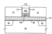
Fig. 6 is the sectional view of Semiconductor substrate part, and it illustrates the illustrative embodiments that has the integrated field-effect transistor isolated transistor cap rock, that have metal silicide gate.As shown in Figure 6, semiconductor device comprises the p type conductive silicon substrate 60 that wherein is formed with transistor isolation district 61 (also being the trench isolations oxide).Transistor gate 140 comprises and the transistor gate isolation cap rock 120 of metal silicide portion 110 stacks that they are superimposed upon successively on the polysilicon segment 141 and with transistor gate oxide 62 and separate.Source/drain region 151 forms in the relative both sides of transistor gate 141.For finishing transistor gate, make the sidewall of transistor gate isolation spacers 150 covering transistor grids.
With reference to Fig. 7-16 the first method embodiment of the present invention is described.Referring now to Fig. 7, substrate 60 is handled, channel separating zone 61 is formed in the conductivity p type silicon substrate 60.On isolated area 61 and substrate 60, form the oxide skin(coating) 62 that finally becomes transistor gate oxide.Then, on oxide skin(coating) 62, form polysilicon layer 70, and on polysilicon layer 70, form trench isolation 71.Trench isolation not only can be a silicon dioxide but also can be silicon nitride, and what select in this first example of the present invention is silicon dioxide.Make photoresist 72 patternings, to provide opening 73, the groove of etching back in this opening permission groove silicon dioxide 71 below.
Referring now to Fig. 8, etched trench 80 in groove silicon dioxide 71, come out up to following polysilicon layer 70.Then, use following silicon 70 as the silicon source, by the known method of those skilled in the art, the epitaxial silicon 81 (epi-Si) of about 400-500 dust of growing in the bottom of groove 80.Apparent from following processing step, the thickness of epitaxial silicon 81 depends on the desirable thickness of the metal silicide that will form.Thickness is that the epitaxial silicon 81 of about 400-500 dust is represented a preferred embodiment of the invention.
Referring now to Fig. 9, on the top surface of groove silicon dioxide 71, have the metal level 90 that thickness is approximately the 40-100 dust with conformal fashion deposition along the sidewall (in groove 80) of silicon dioxide 71 and on the top surface of epitaxial silicon 81, for example nickel or preferred cobalt.In this example of the present invention, select cobalt as metal level 90.After this metal deposition, on metal level, have conductive layer 91 that thickness is approximately 100 dusts for example titanium or titanium nitride with conformal fashion deposition.Metal level 90 and conductive layer 91 are to deposit by the known mode of those skilled in the art.
Referring now to Figure 10 and employing titanium and the preferred example of cobalt conduct, now, titanium layer 91 and cobalt layer 90 are superimposed upon on the epitaxial silicon 81.In order to make cobalt react with epi-Si at first, make semiconductor device stand about 500-600 ℃ interior, about 30 to the 60 seconds annealing steps (being preferably high speed heat treatment (RTP)) of temperature range, to form cobalt silicide 100 (CoSi
x, wherein x changes in 1-2).In this moment of this technology, the epitaxial silicon 81 of a part still keeps.Optionally titanium layer 91 helps control final CoSi2 particle size and orientation by preventing following cobalt caking (caking is its tropism).Help on control CoSi2 orientation of particles and this meaning of size from titanium, titanium constitutes " guiding " layer in fact.Thereby, be preferred based on the existence of the layer (also being titanium or titanium nitride) of titanium, although titanium layer 91 is optionally, even and use, it also will peel off in the technology of back.
Referring now to Figure 11,,, the cobalt 90 of non-reacted parts and titanium 91 are peeled off from semiconductor surface, thereby only stayed CoSi by ammoniacal liquor peroxide mixture (APM) or hydrochloric acid peroxide mixture (HPM) in case the annealing steps of front is finished
x110 and epitaxial silicon 81 in groove.
Can make this semiconductor device stand optional second annealing steps about 800-900 ℃, about 30 to 60 seconds then, be preferably the RTP step, with the CoSi that guarantees to contact with epitaxial silicon 81
x100 really with the reaction of following epitaxial silicon, have the whole CoSi that thickness is approximately the 100-350 dust thereby form
2Layer 110.For having the epi-Si layer 81 (this be situation in the present invention) of thickness, the thickness decision CoSi of cobalt layer 90 greater than CoSi2 layer 110 desirable thickness
2The gross thickness of layer 110.Desirable is to form CoSi
2After the layer 110, a part of epitaxial silicon 81 is retained in the bottom of groove 73 and above the initial surface of polysilicon layer 70, to guarantee not have the polysilicon 70 of metal silicide below invading.
If allow CoSi
2 Polysilicon layer 70 below invading is so as discussing this CoSi in the prior art
2Also isotropic ground is formed (at vertical and horizontal both direction), and the width of gate stack will grow into outside the width of groove 80, thereby cause of the restriction of the characteristic size of gate stack greater than the critical dimension of given technology.This situation causes critical dimension control to incur loss; Because can not utilize typical gate stack etch chemistry reagent to come etching CoSi
2
Referring now to Figure 12, deposition isolation cap 120 for example silicon nitride or silicon dioxide with the remaining area of filling groove 80 fully.This class isolated material that is deposited depends on the type of the isolated material that is used to form groove.In this example, the trench isolation of use is a silicon dioxide, thereby to select the isolated material 120 in order to fill this groove are silicon nitrides, and is apparent in its reason step below.
Referring now to Figure 13, on the surface of trench isolation 71 (silicon dioxide) or the below isolation cap 120 (silicon nitride) is carried out dark etching, to remove its side direction part.This etching is optionally to earth silicon material 71, and also promptly this is etched in when in a single day it reach earth silicon material 71 and stops.For example, can adopt chemical-mechanical planarization etching, it can stop on earth silicon material 71.
Referring now to Figure 14, isolation cap 120 is carried out optionally etching, remove isolated groove material 71, that part of polysilicon layer 70 and gate oxide level below isolated groove material 71, to form transistor gate stack 140.Transistor stack material can only be utilized dry ecthing or carry out etching in conjunction with wet etching, to remove trench material, then removes polysilicon and gate oxide by dry ecthing.Transistor gate stack 140 comprises gate cap 120, CoSi
2 Part 110, epitaxial silicon part 81 and polysilicon segment 70 (they combine and form silicon part 141) and gate oxide part 62.After forming gate stack 140, implement the N type and inject, to form light dope autoregistration source/drain region 142.
Referring now to Figure 15, at the sidewall formation transistor gate sept 150 of gate stack 140.Then, implement the N type and inject, with formation source/drain region 151.Then, finish this semiconductor device with the known suitable manufacturing process of those skilled in the art.
Figure 16 draws the vertical view of the complete transistor arrangement among Figure 15, and it illustrates transistor gate stack 140, transistor gate sept 150, source-drain area 151 and transistor grooves isolated area 61.
With reference to Fig. 7 and 17-26 the present invention second method embodiment is described.Referring now to Fig. 7, substrate 60 is handled, make in conductivity p type silicon substrate 60, to form channel separating zone 61.Form oxide skin(coating) 62 on isolated area 61 and substrate 60, it becomes transistor gate oxide the most at last.Then, on oxide skin(coating) 62, form polysilicon layer 70, and on polysilicon layer 70, form trench isolation 71.Trench isolation both can be a silicon dioxide, can be again silicon nitride, and what select in this second example of the present invention is silicon nitride.Make photoresist 72 patternings, so that opening 73 to be provided, this opening will allow groove that forms subsequently of etching in below the groove silicon nitride 71.
Referring now to Figure 17, etched trench 170 in groove silicon nitride 71, till following polysilicon layer 70 comes out.Then, forming the conformal isolated material 171 of one deck on the trench isolation 71, along the exposed sidewalls (staying the inside of groove 170) of trench isolation 71 and on the expose portion of polysilicon layer 70.Preferably, isolated material 171 is the dielectric materials with trench isolation 71 same types, so that can remove isolated material 171 when this trench isolation 71 of selective etch.In this example, because selected trench isolation is a silicon nitride, therefore also silicon nitride is used as isolated material 171.
Referring now to Figure 18, carry out spacer-etch, to form along the silicon nitride trench spacers 171 of the sidewall of groove 170.Then, the polysilicon 70 below utilizing by the known method of those skilled in the art, is approximately the epitaxial silicon 180 (epi-Si) of 400-500 dust as the source at the bottom of groove 170 growth thickness.Apparent from the last stages of this technology; the existence of inboard nitride spacer 171 will allow to produce the transistor that has than the littler feature that can obtain by the critical dimension restriction of given technology, and provide protection for the metal silicide of formation subsequently.
Referring now to Figure 19, on the top surface of groove silicon nitride 171, along the sidewall of silicon nitride 171 and the metal level 190 for example nickel or the preferred cobalt that on the top surface of epitaxial silicon 180, have the thickness of about 40-100 dust with conformal fashion deposition.In this example of the present invention, select cobalt as metal level 190.Follow after this metal deposition, the optional conductive layer 191 that has about 100 dusts of thickness with conformal fashion deposition on metal level 190 is titanium or titanium nitride for example.Metal level 190 and conductive layer 191 are to deposit by the known method of those skilled in the art.
Referring now to Figure 20 and adopt titanium and cobalt as preferred example, now, titanium layer 191 and cobalt layer 190 are superimposed upon on the epitaxial silicon 180.In order to make this cobalt begin and the epitaxial silicon reaction, make this semiconductor device through annealing steps (preferably high speed heat treatment (RTP) step) in about 500-600 ℃ the temperature range, about 30 to 60 seconds, to form cobalt silicide (CoSi
xWherein x changes in 1-2).In this moment of this technology, a part of epitaxial silicon 180 still is retained in the bottom of groove 170.Titanium layer 191 helps control final CoSi2 particle size and orientation by preventing following cobalt caking (caking is its tropism).Help on control CoSi2 orientation of particles and this meaning of size from titanium, titanium constitutes " guiding " layer in fact.Thereby, be preferred based on the existence of the layer (also being titanium or titanium nitride) of titanium, although titanium layer 91 is optionally, even use, it also will peel off in the technology of back.
Referring now to Figure 21,,, the cobalt 90 of non-reacted parts and titanium 91 are peeled off from semiconductor surface, thereby only stayed CoSi by ammoniacal liquor peroxide mixture (APM) or hydrochloric acid peroxide mixture (HPM) in case the annealing steps of front is finished
x200 and epitaxial silicon 180 in groove.
Make this semiconductor device stand about 800-900 ℃, about 30 to 60 seconds optional second annealing steps then, be preferably the RTP step, with the CoSi that guarantees to contact with epitaxial silicon 180
x200 really with the reaction of following epitaxial silicon, have the CoSi that thickness is approximately the 100-350 dust thereby form
2Layer 210.For having thickness greater than CoSi
2The silicon epitaxial layers 180 (this is the situation among the present invention) of layer 210 desirable thickness, the thickness decision CoSi of cobalt layer 190
2The gross thickness of layer 210.Desirable is to form CoSi
2After the layer 210, a part of epitaxial silicon 180 is retained in the bottom of groove 170, and above the initial surface of polysilicon layer 70, to guarantee not have CoSi
2Polysilicon 70 below invading.
As mentioned in first embodiment of the invention, if allow CoSi
2Polysilicon layer 70 below invading is so as discussing this CoSi in the prior art
2Also isotropic ground is formed (at vertical and horizontal both direction), and the width of gate stack will grow into outside the width of groove 170, this makes the characteristic size of gate stack greater than the restriction of the critical dimension of given technology.This situation causes critical dimension control to incur loss, because can not utilize typical gate stack etch chemistry reagent to come etching CoSi
2
Referring now to Figure 22, deposition isolation cap 220 is silicon nitride or silicon dioxide for example, with the remaining area of complete filling groove 170.This class isolated material that is deposited depends on the type of the isolated material that is used to form groove.In this example, the trench isolation of use is a silicon nitride, thereby to select the isolated material 220 in order to fill this groove be silicon dioxide, and is apparent in its reason step below.
Referring now to Figure 23, on the surface of trench isolation 71 (silicon nitride) or the below isolation cap 220 (silicon dioxide) is carried out dark etching, to remove its side direction part.This etching is optionally to silicon nitride material 71, and also promptly this is etched in when in a single day it reach silicon nitride material 71 and stops.For example, can adopt chemical-mechanical planarization etching, it can stop on silicon nitride material 71.
Referring now to Figure 24, isolation cap 220 is carried out optionally etching, remove isolated groove material 71, that part of polysilicon layer 70 and gate oxide level below isolated groove material 71, to form transistor gate stack 240.Transistor stack material can only be utilized dry ecthing or carry out etching in conjunction with wet etching, removing trench material, and removes polysilicon and gate oxide by dry ecthing.Transistor gate stack 240 comprises gate cap 220, CoSi
2 Part 210, epitaxial silicon part 180 and polysilicon segment 70 (they combine and form silicon part 241) and gate oxide part 70.The existence of trench spacers 171 and removal subsequently can make the characteristic size of transistor gate stack reduce the thickness of trench spacers 171.Use trench spacers to make transistor gate stack and will realize bigger manufacturing flexibility effectively.After forming gate stack 240, implement the N type and inject, to form light dope autoregistration source/drain region 242.
Referring now to Figure 25, at the sidewall formation transistor gate sept 250 of gate stack 240.Then, implement the N type and inject, with formation source/drain region 251.Then, finish this semiconductor device with the known suitable manufacturing process of those skilled in the art.
Figure 26 draws the vertical view of the complete transistor arrangement among Figure 25, and it has transistor gate stack 240, transistor gate sept 250, source-drain area 251 and transistor grooves isolated area 61.
These exemplary embodiments with reference to be formed for semiconductor device for example the transistor arrangement of memory device discuss.Yet those skilled in the art can use the scheme of being instructed in these exemplary embodiments and be formed for transistor arrangement in all semiconductor application.For example, the present invention can be applied in the semiconductor system system that for example Figure 27 drew, its general operational circumstances is known to those skilled in the art.
Figure 27 represents the general block diagram of a semiconductor system, it comprises processor 270 and memory 271, show to store integrated circuit for example row address buffer district 273 and row memory buffer 274, row decoder 275 and column decoder 276, sense amplifier 277, essential parts such as storage array 278 and data I/O 279, they are controlled by controlling 272 by the control/timing signal of from processor.
Be appreciated that, although the present invention describes with reference to two exemplary embodiments, but to structure disclosed herein and technology, can be under the precursor that does not break away from as the invention of the description of appended some claims, structure known various change concerning those skilled in the art are routine.
Claims (22)
1. transistorized method that forms in the semiconductor device comprises:
Silicon substrate material is provided, transistor gate oxide layer and silicon layer are arranged on described silicon substrate material;
Form groove in the isolated material on being superimposed upon described silicon layer;
Be formed at silicon and metal in the described groove;
Make described metal and described pasc reaction,, prevent that simultaneously the described silicon layer outside being arranged in the described border of described groove from forming metal silicide in the border of described groove, to form metal silicide;
On described metal silicide, form transistor isolation cap;
Remove described isolated material and following silicon layer and the zone of transistor gate oxide, comprise the transistor gate stack of the part of described transistor isolation cap, described metal silicide, described silicon layer and described transistor gate oxide with formation; And
On described silicon substrate material and relative both sides, form described transistorized source/drain region in described transistor gate stack.
2. the method for claim 1 wherein forms metal silicide and also comprises:
The epitaxial silicon material is formed on the bottom at the described groove that contacts with described silicon layer;
In described groove and on described epitaxial silicon material, form metal level;
Directly on metal level, form the compound layer of titanium or titanium; And
With the annealing of described semiconductor device, so that described metal level and the reaction of described silicon materials and form described metal silicide.
3. the method for claim 1 also comprises:
In described groove, form before the described metal silicide, on the sidewall of the described isolated material that forms by described groove, form the internal channel sept.
4. the method for claim 1, wherein said metal level comprises cobalt or nickel.
5. method as claimed in claim 2, the compound layer of wherein said titanium or titanium comprises titanium or titanium nitride.
6. the method for claim 1, wherein said metal silicide comprises CoSi
x, wherein x changes in 1-2.
7. the method for claim 1, wherein said metal silicide comprises cobalt silicide or nickle silicide.
8. transistorized method that forms in the semiconductor device comprises:
Be provided at the substrate that is formed with isolated area in the conductive silicon substrate, be formed with oxide skin(coating) on the described substrate;
On described oxide skin(coating), form polysilicon layer;
On described polysilicon layer, form trench isolation;
On described trench isolation, form the photoresist of the patterning that wherein has opening;
In described trench isolation, etch groove by described opening, and expose the part of following polysilicon layer;
Grow epitaxial silicon in the bottom of described groove on the described expose portion of the polysilicon layer below described;
Along the sidewall of described groove and on described epitaxial silicon depositing metal layers;
Described semiconductor device is implemented first annealing, so that described metal level and the reaction of described epitaxial silicon, thereby metal silicide formed;
Remove any unreacted metal layer;
Implement second annealing steps, so that the formation of metal silicide is proceeded;
In described groove and on described metal silicide, deposit isolation cap;
Remove the side direction part of described isolation cap;
The described isolation cap of etching optionally comprises the transistor gate stack of the part of transistor isolation cap, described metal silicide, described silicon layer and described transistor gate oxide with formation;
Conductive impurities is injected described conductive silicon substrate, to form described transistorized autoregistration lightly-doped source/drain region;
Form transistor gate sidewall isolation spacer; And
Conductive impurities is injected described conductive silicon substrate, to form described transistorized source/drain region.
9. method as claimed in claim 8, wherein said metal level comprises cobalt or nickel.
10. method as claimed in claim 8 also comprises:
Before epitaxial silicon growth is arrived the bottom of described groove, on the sidewall of the described trench isolation that forms by described groove, form the internal channel sept.
11. method as claimed in claim 10 also comprises:
During removing described isolation cap, remove described internal channel sept.
12. method as claimed in claim 8 also comprises:
Depositing conducting layer on described metal level is with the formation of control metal silication composition granule; And
During removing any unreacted metal silicide, remove described conductive layer.
13. a formation has the method for transistorized semiconductor storage unit, comprising:
Be provided at the substrate that is formed with isolated area in the conductive silicon substrate, be formed with oxide skin(coating) on the described substrate;
On described oxide skin(coating), form polysilicon layer;
On described polysilicon layer, form trench isolation;
On described trench isolation, form the photoresist of the patterning that wherein has opening;
In described trench isolation, etch groove by described opening, and expose the part of following polysilicon layer;
Grow epitaxial silicon in the bottom of described groove on the described expose portion of the polysilicon layer below described;
Along the sidewall of described groove and on described epitaxial silicon depositing metal layers;
Described semiconductor device is implemented first annealing, so that described metal level and the reaction of described epitaxial silicon, thereby metal silicide formed;
Remove any unreacted metal layer;
Implement second annealing steps, so that the formation of metal silicide is proceeded;
In described groove and on described metal silicide, deposit isolation cap;
Remove the side direction part of described isolation cap;
The described isolation cap of etching optionally comprises the transistor gate stack of the part of transistor isolation cap, described metal silicide, described silicon layer and described transistor gate oxide with formation;
Conductive impurities is injected described conductive silicon substrate, to form described transistorized autoregistration lightly-doped source/drain region;
Form transistor gate sidewall isolation spacer; And
Conductive impurities is injected described conductive silicon substrate, to form described transistorized source/drain region.
14. method as claimed in claim 13, wherein said metal level comprises cobalt or nickel.
15. method as claimed in claim 13 also comprises:
Before epitaxial silicon growth is arrived the bottom of described groove, on the sidewall of the described trench isolation that forms by described groove, form the internal channel sept.
16. method as claimed in claim 15 also comprises:
During removing described isolation cap, remove described internal channel sept.
17. method as claimed in claim 13 also comprises:
Depositing conducting layer on described metal level is with the formation of control metal silication composition granule; And
During removing any unreacted metal silicide, remove described conductive layer.
18. method of using the method formation semiconductor subassembly in the claim 13.
19. method of using the method formation semiconductor system in the claim 13.
20. a method that is formed for the transistor gate of field-effect transistor comprises:
Be provided at the substrate that is formed with isolated area in the conductive silicon substrate, be formed with oxide skin(coating) on the described substrate;
On described oxide skin(coating), form polysilicon layer;
On described polysilicon layer, form trench isolation;
On described trench isolation, form the photoresist of the patterning that wherein has opening;
In described trench isolation, etch groove by described opening, and expose the part of following polysilicon layer;
Grow the epitaxial silicon that thickness is the 400-500 dust on the described expose portion of the polysilicon layer below described, in the bottom of described groove;
Along the sidewall of described groove and on described epitaxial silicon deposit cobalt layers;
On described cobalt layer, deposit titanium layer;
Described semiconductor device is implemented first annealing in the 500-600 ℃ of temperature range, 30 to 60 seconds, so that described cobalt layer and the reaction of described epitaxial silicon, thereby cobalt silicide formed;
Remove any unreacted titanium layer and cobalt layer;
Described semiconductor device stands in the 800-900 ℃ of temperature range by making, 30 to 60 seconds rapid thermal treatment step, implement second annealing steps, with further formation cobalt silicide, make that described cobalt silicide thicknesses is the 100-350 dust, but can not invade in the following polysilicon layer part;
In described groove and on described cobalt silicide, deposit isolation cap;
Optionally etching is to remove the side direction part of described isolation cap;
The described isolation cap of etching optionally comprises the transistor gate stack of the part of transistor isolation cap, described cobalt silicide, described polysilicon and described transistor gate oxide with formation;
Inject conductive impurities, to form described transistorized autoregistration lightly-doped source/drain region;
Form transistor gate sidewall isolation spacer; And
Inject conductive impurities, to form described transistorized source/drain region.
21. method as claimed in claim 20 also comprises:
Before epitaxial silicon growth is arrived the bottom of described groove, on the sidewall of the described trench isolation that forms by described groove, form the internal channel sept.
22. method as claimed in claim 21 also comprises:
During removing described isolation cap, remove described internal channel sept.
Applications Claiming Priority (2)
| Application Number | Priority Date | Filing Date | Title |
|---|---|---|---|
| US10/641,851 | 2003-08-15 | ||
| US10/641,851 US7012024B2 (en) | 2003-08-15 | 2003-08-15 | Methods of forming a transistor with an integrated metal silicide gate electrode |
Publications (2)
| Publication Number | Publication Date |
|---|---|
| CN1868047A CN1868047A (en) | 2006-11-22 |
| CN100421226C true CN100421226C (en) | 2008-09-24 |
Family
ID=34136456
Family Applications (1)
| Application Number | Title | Priority Date | Filing Date |
|---|---|---|---|
| CNB2004800304590A Active CN100421226C (en) | 2003-08-15 | 2004-08-04 | Methods of forming a transistor with an integrated metal silicide gate electrode |
Country Status (9)
| Country | Link |
|---|---|
| US (2) | US7012024B2 (en) |
| EP (1) | EP1656696B1 (en) |
| JP (1) | JP4826914B2 (en) |
| KR (1) | KR100669627B1 (en) |
| CN (1) | CN100421226C (en) |
| AT (1) | ATE465511T1 (en) |
| DE (1) | DE602004026737D1 (en) |
| TW (1) | TWI245418B (en) |
| WO (1) | WO2005020282A2 (en) |
Families Citing this family (23)
| Publication number | Priority date | Publication date | Assignee | Title |
|---|---|---|---|---|
| US7012024B2 (en) | 2003-08-15 | 2006-03-14 | Micron Technology, Inc. | Methods of forming a transistor with an integrated metal silicide gate electrode |
| KR100555541B1 (en) * | 2003-12-23 | 2006-03-03 | 삼성전자주식회사 | Forming method for cobalt silicide layer and manufacturing method for semiconductor device using the forming method |
| US7120046B1 (en) * | 2005-05-13 | 2006-10-10 | Micron Technology, Inc. | Memory array with surrounding gate access transistors and capacitors with global and staggered local bit lines |
| US7371627B1 (en) * | 2005-05-13 | 2008-05-13 | Micron Technology, Inc. | Memory array with ultra-thin etched pillar surround gate access transistors and buried data/bit lines |
| US7888721B2 (en) * | 2005-07-06 | 2011-02-15 | Micron Technology, Inc. | Surround gate access transistors with grown ultra-thin bodies |
| US7768051B2 (en) * | 2005-07-25 | 2010-08-03 | Micron Technology, Inc. | DRAM including a vertical surround gate transistor |
| US7696567B2 (en) * | 2005-08-31 | 2010-04-13 | Micron Technology, Inc | Semiconductor memory device |
| US7875959B2 (en) * | 2005-08-31 | 2011-01-25 | Taiwan Semiconductor Manufacturing Company, Ltd. | Semiconductor structure having selective silicide-induced stress and a method of producing same |
| US7867845B2 (en) * | 2005-09-01 | 2011-01-11 | Micron Technology, Inc. | Transistor gate forming methods and transistor structures |
| US7678607B2 (en) | 2007-02-05 | 2010-03-16 | Intermolecular, Inc. | Methods for forming resistive switching memory elements |
| US7972897B2 (en) | 2007-02-05 | 2011-07-05 | Intermolecular, Inc. | Methods for forming resistive switching memory elements |
| US7704789B2 (en) | 2007-02-05 | 2010-04-27 | Intermolecular, Inc. | Methods for forming resistive switching memory elements |
| WO2008109199A1 (en) * | 2007-03-05 | 2008-09-12 | Intermolecular, Inc. | Methods for forming nonvolatile memory elements with resistive-switching metal oxides |
| US7629198B2 (en) | 2007-03-05 | 2009-12-08 | Intermolecular, Inc. | Methods for forming nonvolatile memory elements with resistive-switching metal oxides |
| US8097878B2 (en) | 2007-03-05 | 2012-01-17 | Intermolecular, Inc. | Nonvolatile memory elements with metal-deficient resistive-switching metal oxides |
| WO2008140979A1 (en) | 2007-05-09 | 2008-11-20 | Intermolecular, Inc. | Resistive-switching nonvolatile memory elements |
| KR101482814B1 (en) | 2007-07-25 | 2015-01-14 | 인터몰레큘러 인코퍼레이티드 | Multistate nonvolatile memory elements |
| WO2009015298A2 (en) | 2007-07-25 | 2009-01-29 | Intermolecular, Inc. | Nonvolatile memory elements |
| US20090236675A1 (en) * | 2008-03-21 | 2009-09-24 | National Tsing Hua University | Self-aligned field-effect transistor structure and manufacturing method thereof |
| KR101604054B1 (en) * | 2009-09-03 | 2016-03-16 | 삼성전자주식회사 | Semiconductor devices and methods of forming thereof |
| US8030196B2 (en) * | 2010-01-12 | 2011-10-04 | Samsung Electronics Co., Ltd. | Transistor formation using capping layer |
| CN113594237B (en) * | 2020-04-30 | 2023-09-26 | 长鑫存储技术有限公司 | Buried gate manufacturing method and semiconductor device manufacturing method |
| CN111739839B (en) * | 2020-06-23 | 2021-07-02 | 武汉新芯集成电路制造有限公司 | Method for manufacturing self-aligned contact hole and method for manufacturing semiconductor device |
Citations (4)
| Publication number | Priority date | Publication date | Assignee | Title |
|---|---|---|---|---|
| CN1175321A (en) * | 1994-12-23 | 1998-03-04 | 英特尔公司 | Novel transistor with ultra shallow tip and method of fabrication |
| US6177333B1 (en) * | 1999-01-14 | 2001-01-23 | Micron Technology, Inc. | Method for making a trench isolation for semiconductor devices |
| US6362086B2 (en) * | 1998-02-26 | 2002-03-26 | Micron Technology, Inc. | Forming a conductive structure in a semiconductor device |
| CN1351370A (en) * | 2000-10-30 | 2002-05-29 | 世界先进积体电路股份有限公司 | Technology for preparing MOS FET with embedded grid |
Family Cites Families (21)
| Publication number | Priority date | Publication date | Assignee | Title |
|---|---|---|---|---|
| FR2652448B1 (en) * | 1989-09-28 | 1994-04-29 | Commissariat Energie Atomique | METHOD FOR MANUFACTURING A HIGH VOLTAGE INTEGRATED CIRCUIT. |
| US5923971A (en) * | 1996-10-22 | 1999-07-13 | International Business Machines Corporation | Reliable low resistance strap for trench storage DRAM cell using selective epitaxy |
| JPH11204791A (en) * | 1997-11-17 | 1999-07-30 | Toshiba Corp | Semiconductor device and its manufacture |
| US6177699B1 (en) * | 1998-03-19 | 2001-01-23 | Lsi Logic Corporation | DRAM cell having a verticle transistor and a capacitor formed on the sidewalls of a trench isolation |
| US6107154A (en) * | 1998-05-12 | 2000-08-22 | United Microelectronics Corp. | Method of fabricating a semiconductor embedded dynamic random-access memory device |
| IL143078A0 (en) * | 1998-11-12 | 2002-04-21 | Intel Corp | Field effect transistor structure with abrupt source/drain junctions |
| US6358788B1 (en) | 1999-08-30 | 2002-03-19 | Micron Technology, Inc. | Method of fabricating a wordline in a memory array of a semiconductor device |
| US6372618B2 (en) * | 2000-01-06 | 2002-04-16 | Micron Technology, Inc. | Methods of forming semiconductor structures |
| US6346477B1 (en) * | 2001-01-09 | 2002-02-12 | Research Foundation Of Suny - New York | Method of interlayer mediated epitaxy of cobalt silicide from low temperature chemical vapor deposition of cobalt |
| US6388327B1 (en) * | 2001-01-09 | 2002-05-14 | International Business Machines Corporation | Capping layer for improved silicide formation in narrow semiconductor structures |
| JP3992439B2 (en) * | 2001-01-16 | 2007-10-17 | 株式会社ルネサステクノロジ | Manufacturing method of semiconductor device |
| US6406962B1 (en) * | 2001-01-17 | 2002-06-18 | International Business Machines Corporation | Vertical trench-formed dual-gate FET device structure and method for creation |
| US6458679B1 (en) * | 2001-02-12 | 2002-10-01 | Advanced Micro Devices, Inc. | Method of making silicide stop layer in a damascene semiconductor structure |
| US6498062B2 (en) * | 2001-04-27 | 2002-12-24 | Micron Technology, Inc. | DRAM access transistor |
| DE10126579C2 (en) * | 2001-05-31 | 2003-12-11 | Infineon Technologies Ag | Method for producing a gate stack in ultra-high-integrated semiconductor memories |
| US20030011018A1 (en) * | 2001-07-13 | 2003-01-16 | Hurley Kelly T. | Flash floating gate using epitaxial overgrowth |
| KR100418928B1 (en) * | 2001-10-24 | 2004-02-14 | 주식회사 하이닉스반도체 | Method for fabricating of Merged DRAM with Logic semiconductor device |
| US6657223B1 (en) * | 2002-10-29 | 2003-12-02 | Advanced Micro Devices, Inc. | Strained silicon MOSFET having silicon source/drain regions and method for its fabrication |
| US7132065B2 (en) | 2003-02-12 | 2006-11-07 | 3M Innovative Properties Company | Process for manufacturing polymeric optical film |
| KR100538806B1 (en) * | 2003-02-21 | 2005-12-26 | 주식회사 하이닉스반도체 | SEMICONDUCTOR DEVICE WITH EPITAXIAL C49-TiSi2 LAYER AND METHOD FOR FABRICATING THE SAME |
| US7012024B2 (en) | 2003-08-15 | 2006-03-14 | Micron Technology, Inc. | Methods of forming a transistor with an integrated metal silicide gate electrode |
-
2003
- 2003-08-15 US US10/641,851 patent/US7012024B2/en not_active Expired - Fee Related
-
2004
- 2004-08-04 CN CNB2004800304590A patent/CN100421226C/en active Active
- 2004-08-04 EP EP04786450A patent/EP1656696B1/en active Active
- 2004-08-04 WO PCT/US2004/025085 patent/WO2005020282A2/en active IP Right Grant
- 2004-08-04 AT AT04786450T patent/ATE465511T1/en not_active IP Right Cessation
- 2004-08-04 JP JP2006523875A patent/JP4826914B2/en active Active
- 2004-08-04 KR KR1020067003171A patent/KR100669627B1/en active IP Right Grant
- 2004-08-04 DE DE602004026737T patent/DE602004026737D1/en active Active
- 2004-08-05 TW TW093123459A patent/TWI245418B/en active
-
2005
- 2005-09-30 US US11/241,517 patent/US7351659B2/en not_active Expired - Lifetime
Patent Citations (4)
| Publication number | Priority date | Publication date | Assignee | Title |
|---|---|---|---|---|
| CN1175321A (en) * | 1994-12-23 | 1998-03-04 | 英特尔公司 | Novel transistor with ultra shallow tip and method of fabrication |
| US6362086B2 (en) * | 1998-02-26 | 2002-03-26 | Micron Technology, Inc. | Forming a conductive structure in a semiconductor device |
| US6177333B1 (en) * | 1999-01-14 | 2001-01-23 | Micron Technology, Inc. | Method for making a trench isolation for semiconductor devices |
| CN1351370A (en) * | 2000-10-30 | 2002-05-29 | 世界先进积体电路股份有限公司 | Technology for preparing MOS FET with embedded grid |
Also Published As
| Publication number | Publication date |
|---|---|
| KR100669627B1 (en) | 2007-01-16 |
| TW200511572A (en) | 2005-03-16 |
| US20050037584A1 (en) | 2005-02-17 |
| DE602004026737D1 (en) | 2010-06-02 |
| EP1656696A2 (en) | 2006-05-17 |
| US7012024B2 (en) | 2006-03-14 |
| JP4826914B2 (en) | 2011-11-30 |
| TWI245418B (en) | 2005-12-11 |
| EP1656696B1 (en) | 2010-04-21 |
| WO2005020282A3 (en) | 2006-02-09 |
| JP2007503116A (en) | 2007-02-15 |
| US7351659B2 (en) | 2008-04-01 |
| WO2005020282A2 (en) | 2005-03-03 |
| ATE465511T1 (en) | 2010-05-15 |
| EP1656696A4 (en) | 2008-07-23 |
| CN1868047A (en) | 2006-11-22 |
| KR20060032662A (en) | 2006-04-17 |
| US20060019457A1 (en) | 2006-01-26 |
Similar Documents
| Publication | Publication Date | Title |
|---|---|---|
| CN100421226C (en) | Methods of forming a transistor with an integrated metal silicide gate electrode | |
| US7696032B2 (en) | Semiconductor device including a crystal semiconductor layer, its fabrication and its operation | |
| US5915183A (en) | Raised source/drain using recess etch of polysilicon | |
| US7329924B2 (en) | Integrated circuits and methods of forming a field effect transistor | |
| KR100714401B1 (en) | Semiconductor device having stacked transistors and method of forming the same | |
| US7670912B2 (en) | Methods of fabricating multichannel metal oxide semiconductor (MOS) transistors | |
| KR100474150B1 (en) | Fully encapsulated damascene gates for gigabit drams | |
| JP2005072577A (en) | High integration semiconductor device provided with silicide film capable of assuring contact margin, and manufacturing method therefor | |
| JP2000260953A (en) | Gate device having expanded contact area for source and drain terminals and its manufacture | |
| JP2001085637A (en) | Vertical dram cell having word line self-aligned with storage trench | |
| JP2000216386A (en) | Fabrication of semiconductor device having junction | |
| JP2002231727A (en) | SiGe HETEROJUNCTION BIPOLAR TRANSISTOR AND METHOD OF MANUFACTURING THE SAME | |
| US6207492B1 (en) | Common gate and salicide word line process for low cost embedded DRAM devices | |
| JPH1041412A (en) | Semiconductor device and its manufacture | |
| US20050006724A1 (en) | Bicmos structure, method for producing the same and bipolar transistor for a bicmos structure | |
| KR100706918B1 (en) | Memory cell comprising a trench and method for production thereof | |
| US7485558B2 (en) | Method of manufacturing semiconductor device | |
| JPH10189915A (en) | Process of forming metal silicide gate for dynamic random access memory | |
| KR100664328B1 (en) | A method of manufacturing a semiconductor device | |
| US6291330B1 (en) | Method of fabricating gate structure to reduce stress production | |
| KR100688714B1 (en) | Method for manufacturing transistor | |
| JP2006114686A (en) | Semiconductor device and its manufacturing method | |
| JPH10125622A (en) | Semiconductor device and its method of manufacturing the same | |
| JP2005175210A (en) | Semiconductor device and its fabricating process | |
| JPH11176963A (en) | Semiconductor device and its manufacture |
Legal Events
| Date | Code | Title | Description |
|---|---|---|---|
| C06 | Publication | ||
| PB01 | Publication | ||
| C10 | Entry into substantive examination | ||
| SE01 | Entry into force of request for substantive examination | ||
| C14 | Grant of patent or utility model | ||
| GR01 | Patent grant |