CN100339961C - Integrated circuit device and method therefor - Google Patents
Integrated circuit device and method therefor Download PDFInfo
- Publication number
- CN100339961C CN100339961C CNB038062992A CN03806299A CN100339961C CN 100339961 C CN100339961 C CN 100339961C CN B038062992 A CNB038062992 A CN B038062992A CN 03806299 A CN03806299 A CN 03806299A CN 100339961 C CN100339961 C CN 100339961C
- Authority
- CN
- China
- Prior art keywords
- dielectric layer
- layer
- semiconductor substrate
- reflection coating
- sidewall spacers
- Prior art date
- Legal status (The legal status is an assumption and is not a legal conclusion. Google has not performed a legal analysis and makes no representation as to the accuracy of the status listed.)
- Expired - Fee Related
Links
- 238000000034 method Methods 0.000 title claims description 38
- 239000000758 substrate Substances 0.000 claims abstract description 81
- 125000006850 spacer group Chemical group 0.000 claims abstract description 72
- 239000004065 semiconductor Substances 0.000 claims abstract description 50
- 238000003475 lamination Methods 0.000 claims description 25
- 239000000203 mixture Substances 0.000 claims description 24
- 150000004767 nitrides Chemical class 0.000 claims description 24
- 239000011248 coating agent Substances 0.000 claims description 23
- 238000000576 coating method Methods 0.000 claims description 23
- 229910021332 silicide Inorganic materials 0.000 claims description 13
- FVBUAEGBCNSCDD-UHFFFAOYSA-N silicide(4-) Chemical group [Si-4] FVBUAEGBCNSCDD-UHFFFAOYSA-N 0.000 claims description 13
- 238000000059 patterning Methods 0.000 claims description 11
- 230000004888 barrier function Effects 0.000 claims description 7
- 229910021417 amorphous silicon Inorganic materials 0.000 claims description 6
- 238000002347 injection Methods 0.000 claims description 5
- 239000007924 injection Substances 0.000 claims description 5
- 238000003860 storage Methods 0.000 claims description 5
- 238000005192 partition Methods 0.000 claims description 2
- 238000001035 drying Methods 0.000 claims 2
- 238000000280 densification Methods 0.000 claims 1
- 238000005530 etching Methods 0.000 abstract description 29
- 239000000463 material Substances 0.000 abstract description 11
- 230000015572 biosynthetic process Effects 0.000 abstract description 8
- 238000009792 diffusion process Methods 0.000 abstract description 5
- 239000006117 anti-reflective coating Substances 0.000 abstract 5
- 239000010410 layer Substances 0.000 description 64
- 238000001039 wet etching Methods 0.000 description 9
- 229910021420 polycrystalline silicon Inorganic materials 0.000 description 7
- 229920005591 polysilicon Polymers 0.000 description 7
- 239000003795 chemical substances by application Substances 0.000 description 6
- 238000001312 dry etching Methods 0.000 description 6
- 239000011229 interlayer Substances 0.000 description 4
- 238000005516 engineering process Methods 0.000 description 3
- 229910052710 silicon Inorganic materials 0.000 description 3
- 239000010703 silicon Substances 0.000 description 3
- NBIIXXVUZAFLBC-UHFFFAOYSA-N Phosphoric acid Chemical group OP(O)(O)=O NBIIXXVUZAFLBC-UHFFFAOYSA-N 0.000 description 2
- 230000000694 effects Effects 0.000 description 2
- 102100033892 Actin-related protein 2/3 complex subunit 5 Human genes 0.000 description 1
- ZAMOUSCENKQFHK-UHFFFAOYSA-N Chlorine atom Chemical compound [Cl] ZAMOUSCENKQFHK-UHFFFAOYSA-N 0.000 description 1
- PXGOKWXKJXAPGV-UHFFFAOYSA-N Fluorine Chemical compound FF PXGOKWXKJXAPGV-UHFFFAOYSA-N 0.000 description 1
- 101000925555 Homo sapiens Actin-related protein 2/3 complex subunit 5 Proteins 0.000 description 1
- 229910000147 aluminium phosphate Inorganic materials 0.000 description 1
- 229910052801 chlorine Inorganic materials 0.000 description 1
- 239000000460 chlorine Substances 0.000 description 1
- 230000002950 deficient Effects 0.000 description 1
- 229910052731 fluorine Inorganic materials 0.000 description 1
- 239000011737 fluorine Substances 0.000 description 1
- 229910052736 halogen Inorganic materials 0.000 description 1
- 150000002367 halogens Chemical class 0.000 description 1
- 238000004519 manufacturing process Methods 0.000 description 1
- 239000000126 substance Substances 0.000 description 1
Images


Classifications
-
- H—ELECTRICITY
- H10—SEMICONDUCTOR DEVICES; ELECTRIC SOLID-STATE DEVICES NOT OTHERWISE PROVIDED FOR
- H10B—ELECTRONIC MEMORY DEVICES
- H10B41/00—Electrically erasable-and-programmable ROM [EEPROM] devices comprising floating gates
- H10B41/40—Electrically erasable-and-programmable ROM [EEPROM] devices comprising floating gates characterised by the peripheral circuit region
-
- H—ELECTRICITY
- H01—ELECTRIC ELEMENTS
- H01L—SEMICONDUCTOR DEVICES NOT COVERED BY CLASS H10
- H01L21/00—Processes or apparatus adapted for the manufacture or treatment of semiconductor or solid state devices or of parts thereof
- H01L21/02—Manufacture or treatment of semiconductor devices or of parts thereof
- H01L21/04—Manufacture or treatment of semiconductor devices or of parts thereof the devices having at least one potential-jump barrier or surface barrier, e.g. PN junction, depletion layer or carrier concentration layer
- H01L21/18—Manufacture or treatment of semiconductor devices or of parts thereof the devices having at least one potential-jump barrier or surface barrier, e.g. PN junction, depletion layer or carrier concentration layer the devices having semiconductor bodies comprising elements of Group IV of the Periodic System or AIIIBV compounds with or without impurities, e.g. doping materials
- H01L21/30—Treatment of semiconductor bodies using processes or apparatus not provided for in groups H01L21/20 - H01L21/26
- H01L21/31—Treatment of semiconductor bodies using processes or apparatus not provided for in groups H01L21/20 - H01L21/26 to form insulating layers thereon, e.g. for masking or by using photolithographic techniques; After treatment of these layers; Selection of materials for these layers
- H01L21/3105—After-treatment
- H01L21/311—Etching the insulating layers by chemical or physical means
- H01L21/31105—Etching inorganic layers
- H01L21/31111—Etching inorganic layers by chemical means
- H01L21/31116—Etching inorganic layers by chemical means by dry-etching
-
- H—ELECTRICITY
- H01—ELECTRIC ELEMENTS
- H01L—SEMICONDUCTOR DEVICES NOT COVERED BY CLASS H10
- H01L27/00—Devices consisting of a plurality of semiconductor or other solid-state components formed in or on a common substrate
- H01L27/02—Devices consisting of a plurality of semiconductor or other solid-state components formed in or on a common substrate including semiconductor components specially adapted for rectifying, oscillating, amplifying or switching and having at least one potential-jump barrier or surface barrier; including integrated passive circuit elements with at least one potential-jump barrier or surface barrier
- H01L27/04—Devices consisting of a plurality of semiconductor or other solid-state components formed in or on a common substrate including semiconductor components specially adapted for rectifying, oscillating, amplifying or switching and having at least one potential-jump barrier or surface barrier; including integrated passive circuit elements with at least one potential-jump barrier or surface barrier the substrate being a semiconductor body
- H01L27/10—Devices consisting of a plurality of semiconductor or other solid-state components formed in or on a common substrate including semiconductor components specially adapted for rectifying, oscillating, amplifying or switching and having at least one potential-jump barrier or surface barrier; including integrated passive circuit elements with at least one potential-jump barrier or surface barrier the substrate being a semiconductor body including a plurality of individual components in a repetitive configuration
- H01L27/105—Devices consisting of a plurality of semiconductor or other solid-state components formed in or on a common substrate including semiconductor components specially adapted for rectifying, oscillating, amplifying or switching and having at least one potential-jump barrier or surface barrier; including integrated passive circuit elements with at least one potential-jump barrier or surface barrier the substrate being a semiconductor body including a plurality of individual components in a repetitive configuration including field-effect components
-
- H—ELECTRICITY
- H01—ELECTRIC ELEMENTS
- H01L—SEMICONDUCTOR DEVICES NOT COVERED BY CLASS H10
- H01L29/00—Semiconductor devices adapted for rectifying, amplifying, oscillating or switching, or capacitors or resistors with at least one potential-jump barrier or surface barrier, e.g. PN junction depletion layer or carrier concentration layer; Details of semiconductor bodies or of electrodes thereof ; Multistep manufacturing processes therefor
- H01L29/40—Electrodes ; Multistep manufacturing processes therefor
- H01L29/401—Multistep manufacturing processes
- H01L29/4011—Multistep manufacturing processes for data storage electrodes
- H01L29/40114—Multistep manufacturing processes for data storage electrodes the electrodes comprising a conductor-insulator-conductor-insulator-semiconductor structure
-
- H—ELECTRICITY
- H01—ELECTRIC ELEMENTS
- H01L—SEMICONDUCTOR DEVICES NOT COVERED BY CLASS H10
- H01L29/00—Semiconductor devices adapted for rectifying, amplifying, oscillating or switching, or capacitors or resistors with at least one potential-jump barrier or surface barrier, e.g. PN junction depletion layer or carrier concentration layer; Details of semiconductor bodies or of electrodes thereof ; Multistep manufacturing processes therefor
- H01L29/66—Types of semiconductor device ; Multistep manufacturing processes therefor
- H01L29/66007—Multistep manufacturing processes
- H01L29/66075—Multistep manufacturing processes of devices having semiconductor bodies comprising group 14 or group 13/15 materials
- H01L29/66227—Multistep manufacturing processes of devices having semiconductor bodies comprising group 14 or group 13/15 materials the devices being controllable only by the electric current supplied or the electric potential applied, to an electrode which does not carry the current to be rectified, amplified or switched, e.g. three-terminal devices
- H01L29/66409—Unipolar field-effect transistors
- H01L29/66477—Unipolar field-effect transistors with an insulated gate, i.e. MISFET
- H01L29/665—Unipolar field-effect transistors with an insulated gate, i.e. MISFET using self aligned silicidation, i.e. salicide
-
- H—ELECTRICITY
- H01—ELECTRIC ELEMENTS
- H01L—SEMICONDUCTOR DEVICES NOT COVERED BY CLASS H10
- H01L29/00—Semiconductor devices adapted for rectifying, amplifying, oscillating or switching, or capacitors or resistors with at least one potential-jump barrier or surface barrier, e.g. PN junction depletion layer or carrier concentration layer; Details of semiconductor bodies or of electrodes thereof ; Multistep manufacturing processes therefor
- H01L29/66—Types of semiconductor device ; Multistep manufacturing processes therefor
- H01L29/66007—Multistep manufacturing processes
- H01L29/66075—Multistep manufacturing processes of devices having semiconductor bodies comprising group 14 or group 13/15 materials
- H01L29/66227—Multistep manufacturing processes of devices having semiconductor bodies comprising group 14 or group 13/15 materials the devices being controllable only by the electric current supplied or the electric potential applied, to an electrode which does not carry the current to be rectified, amplified or switched, e.g. three-terminal devices
- H01L29/66409—Unipolar field-effect transistors
- H01L29/66477—Unipolar field-effect transistors with an insulated gate, i.e. MISFET
- H01L29/66545—Unipolar field-effect transistors with an insulated gate, i.e. MISFET using a dummy, i.e. replacement gate in a process wherein at least a part of the final gate is self aligned to the dummy gate
-
- H—ELECTRICITY
- H01—ELECTRIC ELEMENTS
- H01L—SEMICONDUCTOR DEVICES NOT COVERED BY CLASS H10
- H01L29/00—Semiconductor devices adapted for rectifying, amplifying, oscillating or switching, or capacitors or resistors with at least one potential-jump barrier or surface barrier, e.g. PN junction depletion layer or carrier concentration layer; Details of semiconductor bodies or of electrodes thereof ; Multistep manufacturing processes therefor
- H01L29/66—Types of semiconductor device ; Multistep manufacturing processes therefor
- H01L29/66007—Multistep manufacturing processes
- H01L29/66075—Multistep manufacturing processes of devices having semiconductor bodies comprising group 14 or group 13/15 materials
- H01L29/66227—Multistep manufacturing processes of devices having semiconductor bodies comprising group 14 or group 13/15 materials the devices being controllable only by the electric current supplied or the electric potential applied, to an electrode which does not carry the current to be rectified, amplified or switched, e.g. three-terminal devices
- H01L29/66409—Unipolar field-effect transistors
- H01L29/66477—Unipolar field-effect transistors with an insulated gate, i.e. MISFET
- H01L29/6656—Unipolar field-effect transistors with an insulated gate, i.e. MISFET using multiple spacer layers, e.g. multiple sidewall spacers
-
- H—ELECTRICITY
- H01—ELECTRIC ELEMENTS
- H01L—SEMICONDUCTOR DEVICES NOT COVERED BY CLASS H10
- H01L29/00—Semiconductor devices adapted for rectifying, amplifying, oscillating or switching, or capacitors or resistors with at least one potential-jump barrier or surface barrier, e.g. PN junction depletion layer or carrier concentration layer; Details of semiconductor bodies or of electrodes thereof ; Multistep manufacturing processes therefor
- H01L29/66—Types of semiconductor device ; Multistep manufacturing processes therefor
- H01L29/66007—Multistep manufacturing processes
- H01L29/66075—Multistep manufacturing processes of devices having semiconductor bodies comprising group 14 or group 13/15 materials
- H01L29/66227—Multistep manufacturing processes of devices having semiconductor bodies comprising group 14 or group 13/15 materials the devices being controllable only by the electric current supplied or the electric potential applied, to an electrode which does not carry the current to be rectified, amplified or switched, e.g. three-terminal devices
- H01L29/66409—Unipolar field-effect transistors
- H01L29/66477—Unipolar field-effect transistors with an insulated gate, i.e. MISFET
- H01L29/66568—Lateral single gate silicon transistors
- H01L29/66575—Lateral single gate silicon transistors where the source and drain or source and drain extensions are self-aligned to the sides of the gate
- H01L29/6659—Lateral single gate silicon transistors where the source and drain or source and drain extensions are self-aligned to the sides of the gate with both lightly doped source and drain extensions and source and drain self-aligned to the sides of the gate, e.g. lightly doped drain [LDD] MOSFET, double diffused drain [DDD] MOSFET
-
- H—ELECTRICITY
- H01—ELECTRIC ELEMENTS
- H01L—SEMICONDUCTOR DEVICES NOT COVERED BY CLASS H10
- H01L29/00—Semiconductor devices adapted for rectifying, amplifying, oscillating or switching, or capacitors or resistors with at least one potential-jump barrier or surface barrier, e.g. PN junction depletion layer or carrier concentration layer; Details of semiconductor bodies or of electrodes thereof ; Multistep manufacturing processes therefor
- H01L29/66—Types of semiconductor device ; Multistep manufacturing processes therefor
- H01L29/66007—Multistep manufacturing processes
- H01L29/66075—Multistep manufacturing processes of devices having semiconductor bodies comprising group 14 or group 13/15 materials
- H01L29/66227—Multistep manufacturing processes of devices having semiconductor bodies comprising group 14 or group 13/15 materials the devices being controllable only by the electric current supplied or the electric potential applied, to an electrode which does not carry the current to be rectified, amplified or switched, e.g. three-terminal devices
- H01L29/66409—Unipolar field-effect transistors
- H01L29/66477—Unipolar field-effect transistors with an insulated gate, i.e. MISFET
- H01L29/66568—Lateral single gate silicon transistors
- H01L29/66636—Lateral single gate silicon transistors with source or drain recessed by etching or first recessed by etching and then refilled
-
- H—ELECTRICITY
- H01—ELECTRIC ELEMENTS
- H01L—SEMICONDUCTOR DEVICES NOT COVERED BY CLASS H10
- H01L29/00—Semiconductor devices adapted for rectifying, amplifying, oscillating or switching, or capacitors or resistors with at least one potential-jump barrier or surface barrier, e.g. PN junction depletion layer or carrier concentration layer; Details of semiconductor bodies or of electrodes thereof ; Multistep manufacturing processes therefor
- H01L29/66—Types of semiconductor device ; Multistep manufacturing processes therefor
- H01L29/66007—Multistep manufacturing processes
- H01L29/66075—Multistep manufacturing processes of devices having semiconductor bodies comprising group 14 or group 13/15 materials
- H01L29/66227—Multistep manufacturing processes of devices having semiconductor bodies comprising group 14 or group 13/15 materials the devices being controllable only by the electric current supplied or the electric potential applied, to an electrode which does not carry the current to be rectified, amplified or switched, e.g. three-terminal devices
- H01L29/66409—Unipolar field-effect transistors
- H01L29/66477—Unipolar field-effect transistors with an insulated gate, i.e. MISFET
- H01L29/66825—Unipolar field-effect transistors with an insulated gate, i.e. MISFET with a floating gate
-
- H—ELECTRICITY
- H10—SEMICONDUCTOR DEVICES; ELECTRIC SOLID-STATE DEVICES NOT OTHERWISE PROVIDED FOR
- H10B—ELECTRONIC MEMORY DEVICES
- H10B41/00—Electrically erasable-and-programmable ROM [EEPROM] devices comprising floating gates
- H10B41/40—Electrically erasable-and-programmable ROM [EEPROM] devices comprising floating gates characterised by the peripheral circuit region
- H10B41/42—Simultaneous manufacture of periphery and memory cells
- H10B41/43—Simultaneous manufacture of periphery and memory cells comprising only one type of peripheral transistor
Abstract
A semiconductor device (10) has recesses (22) formed in the substrate (12) during removal of the anti-reflective coating (ARC) (16) because these recess locations (22) are exposed during the etching of the ARC (16). Although the etchant is chosen to be selective between the ARC material (16) and the substrate material (12), this selectivity is limited so that recesses (22) do occur. A problem associated with the formation of these recesses is that the source/drains (26, 28) have further to diffuse to become overlapped with the gate (14). The result is that the transistors may have reduced current drive. The problem is avoided by waiting to perform the ARC removal until at least after formation of a sidewall spacer (70) around the gate (64). The consequent recess formation thus occurs further from the gate (64), which results in reducing or eliminating the impediment this recess can cause to the source/drain diffusion (72, 74) that desirably extends to overlap with the gate (64).
Description
Invention field
The present invention relates to integrated circuit, relate in particular to the integrated circuit that in substrate, has recess (recess).
Correlation technique
In the manufacturing of integrated circuit, owing to the size littler more tangible problem that becomes that becomes is a recess in substrate, this recess appears in the standard course of processing.Owing in the process that etches away a part of material layer on substrate, exposed substrate, therefore occurred the recess in the substrate at first.Get rid of be etched the layer process in and/or afterwards, etching agent is applied to substrate the preceding paragraph time.An example is that such position is arranged, when another kind of material in diverse location etching at the beginning, the substrate that exposes is just arranged in this position.Another example is, in the process of the material of other position of etching the thin layer on the substrate carried out etching, and like this, by the material of other position of etching, substrate becomes the part path of exposing.Another example is to etch away the layer on the substrate, and after substrate exposes, proceed etching in the mode of over etching, thereby guarantee the layer that needs are removed is removed fully.Not obvious ground of the etching agent etching semiconductor substrate of desired selection, but in fact this etching agent is very difficult to use.Therefore, removing by the etching agent that Semiconductor substrate (being typically silicon) is not possessed some corrasion need removed layer.This method is shown among Fig. 1-9.
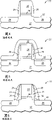
Shown in Figure 1 is a kind of semiconductor device 10 that is used to make integrated circuit, and this semiconductor device 10 comprises the anti-reflection coating (ARC) 16 of substrate 12, polysilicon gate 14, nitride and between grid 14 and substrate 12 and the thin-oxide 18 that extends in the zone adjacent to grid 14.In order to remove nitride ARC16, adopt etching agent, for example based on the material of halogen, as fluorine and chlorine.Though fast unlike the etching nitride, these etching agents are etch silicon also.The result who removes ARC 16 like this is the recessed surfaces 22 shown in Fig. 2.The device 10 that shown in Figure 3 is after forming sidewall spacers 24.Sidewall spacers 24 is formed by oxide, and as well known in the art, sidewall spacers 24 obtains by following manner: the layer of relative conformal is provided, utilizes anisotropic etching that this layer is carried out etching subsequently.This causes another recess that aligns with sidewall spacers 24 in substrate 12.Shown in Figure 4 is regions and source 26 and the source/drain 28 that utilizes sidewall spacers 24 to form as mask.This injection is commonly referred to as extension (extension) and injects, and has the lower doping content of heavy source/drain injection than subsequently.
The device 10 that shown in Figure 9 is formed the silicide area 48 and 50 that extends below zone 40 and 42 after.This shows equally as the zone 49 of the remainder in zone 26 and 28 and 51 diffusion fully.These zones can not extended to all paths of gate oxide 20.Utilize and not exclusively extend to the zone 49 and 51 that contacts with gate oxide 20, have some additional spaces at grid 44 with between the raceway groove that forms between the zone 49 and 51, if therefore between zone 49 and 51 electric current of process be diffused into the electric current of process under the situation that is in close proximity to gate oxide 20 less than them.This is disadvantageous, because the recess of the liner 12 of adjacent gate 44 has directly caused the additional distance of the necessary process of diffusion.Silicide regions 46 also is formed on the top of grid 14, and consumes the grid 14 of significant quantity, thereby stays the grid as the combination of polysilicon region 44 and silicide regions 46.
Therefore, need to reduce having a strong impact on of the recess that in normal process, in substrate, occurs.Along with size reduces, voltage reduces, this problem becomes even worse.If source electrode and drain electrode do not have with on cover the overlapping feature (proper) of grid, inversion channel also provides the ability of optimum current just to be affected between source electrode and drain electrode so fully.
Summary of the invention
According to the present invention, a kind of method that forms integrated circuit (IC)-components on Semiconductor substrate is provided, comprising: form gate stack, this gate stack comprises grid on the gate-dielectric and the anti-reflection coating (ARC) on this grid; Form the first side wall at interval around grid, wherein this sidewall spacers comprises oxide; On sidewall spacers and grid, form liner, and this liner on substrate from the sidewall spacers horizontal expansion; Form second sidewall spacers around grid on liner, wherein this second sidewall spacers comprises nitride, and the part of this liner is between substrate and this second sidewall spacers; And after forming second sidewall spacers, remove ARC.
According to the present invention, a kind of method that forms integrated circuit (IC)-components also is provided, comprising: Semiconductor substrate is set; On Semiconductor substrate, form the composition dielectric layer; On the composition dielectric layer, form patterning conductive layer; On patterning conductive layer, form anti-reflection coating (ARC); On composition dielectric layer and patterning conductive layer, form first dielectric layer; On first dielectric layer, form second dielectric layer; On second dielectric layer, form ground floor; Remove the part ground floor to form first patterned layer, wherein contiguous patterning conductive layer of first patterned layer and composition dielectric layer; Remove part second dielectric to form first dielectric area of contiguous first patterned layer; Remove part first dielectric to form second dielectric area of contiguous first dielectric area; After removing this part first dielectric layer, remove ARC; Form the second layer on ground floor, wherein this second layer comprises amorphous silicon; And optionally remove a part of second layer, thereby form the patterned first of contiguous first patterned layer in the second layer at ground floor.
According to the present invention, a kind of method that forms integrated circuit (IC)-components also is provided, comprising: setting has the Semiconductor substrate of first and second portion; Form gate stack, this gate stack comprises: the gate-dielectric that forms in the first of Semiconductor substrate; With the gate electrode that on gate-dielectric, forms; On gate stack, form the first composition anti-reflection coating (ARC); Form the nonvolatile memory lamination, this lamination comprises: the charge storage layer that forms on the second portion of Semiconductor substrate; With first dielectric layer that on charge storage layer, forms; On the nonvolatile memory lamination, form the second composition ARC; On gate stack and nonvolatile memory lamination, form second dielectric layer; Remove part second dielectric layer to form first interval of adjacent gate lamination and nonvolatile memory lamination; After removing part second dielectric layer, remove the first composition ARC and the second composition ARC; Below gate stack, form first raceway groove; With formation second raceway groove below the nonvolatile memory lamination.
According to the present invention, a kind of integrated circuit (IC)-components also is provided, comprising: Semiconductor substrate; Lamination comprises: the composition dielectric layer that forms on Semiconductor substrate; The patterning conductive layer that on the composition dielectric layer, forms; The first side wall; With second sidewall, wherein second sidewall is relative with the first side wall; The first region at the inner and contiguous the first side wall of Semiconductor substrate; Second electrode district at inner and contiguous second sidewall of Semiconductor substrate; Channel region between the first region and second electrode district and below lamination; The oxide spacer of the contiguous the first side wall and second sidewall, wherein oxide spacer has first height on the top surface of Semiconductor substrate; The nitride spacers of contiguous first oxide spacer, wherein nitride spacers has second height on the top surface of Semiconductor substrate, that be lower than first height; And the insulating barrier between oxide spacer and the nitride spacers, on first and second electrode districts; Wherein this substrate have with oxide spacer and insulating barrier between the recess that aligns of interface.
According to the present invention, a kind of integrated circuit (IC)-components also is provided, comprising: Semiconductor substrate with top surface; The lamination that on Semiconductor substrate, forms, this lamination comprises: ground floor; The second layer that on ground floor, forms; The first side wall; With second sidewall relative with the first side wall; Interval in abutting connection with the first side wall and second sidewall, under wherein the first of the top surface of Semiconductor substrate was positioned at interval, second portion was positioned under the lamination, first basically with the second portion coplane, this has bottom, this bottom whole on the first of Semiconductor substrate at interval; The uniform basically insulating barrier of thickness, its first's adjacent partition, and second portion is directly on the third part of the top surface of Semiconductor substrate, and wherein the third part of the top surface of this Semiconductor substrate falls in respect to the first and the second portion of substrate; First doped region at the inner and contiguous the first side wall of Semiconductor substrate; Second doped region at inner and contiguous second sidewall of Semiconductor substrate; And between first doped region and second doped region and at the channel region of Semiconductor substrate inside.
Description of drawings
Fig. 1-9 expression is according to the continuous cross section of the semiconductor device of original technology.
Figure 10-the 18th, the continuous cross section of the semiconductor device of making according to one embodiment of the invention.
Figure 19-the 25th, make according to another embodiment of the present invention the continuous cross section of semiconductor device.
Embodiment
The problem that has recess in substrate overcomes by following manner, nitride anti-reflection coating (ARC) is removed in wait in technology until subsequently, make the recess that occurs be in close proximity to gate-dielectric and have much smaller influence with gate overlap for source electrode and drain electrode immigration.A kind of mode that realizes is to wait for until being used to shelter the sidewall spacer stack that weighs the source/drain injection being in the appropriate location before removal nitride ARC.As selection, after having formed the sidewall spacers that is used for source/drain extension injection, remove nitride ARC, utilize wet etching to remove nitride ARC in this case.
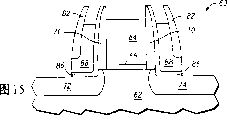
The device 60 that shown in Figure 10 is after forming sidewall spacers 70, alternative as the structure shown in Fig. 2.The structure of Figure 10 is abideed by device architecture shown in Figure 1.Device 60 comprises substrate 62, can be made and as grid 64, the gate oxide 66 of patterning conductive layer type, the ARC 68 that can be nitride and sidewall spacers 70 by polysilicon.The preferred material that is used for substrate 62 is a silicon, and the preferred material that is used for sidewall spacers 70 is an oxide.ARC 68 also can be some other the effective anti-reflection materials outside the nitride.Grid 64 also can be the material outside the polysilicon.Sidewall spacers 70 is by being formed by the oxide skin(coating) of the anisotropic etching of relative conformal.As the result of this anisotropic etching, formed the recess (recess) 71 of substrate 62.This is the result of required over etching, thereby guarantees to get rid of except that the position that forms sidewall spacers, be used to form all layers of sidewall spacers.Owing in over etching, only expose substrate, so recess is smaller.Shown in Figure 11 is extends device 60 after injecting at source/drain, has formed the source/drain regions 72 and the source/drain regions 74 of contiguous sidewall spacers 70 around grid 64.
The device 60 that shown in Figure 12 is after forming liner 76, layer 78 and layer 80. Layer 76,78 and 80 is all typical dielectric substances.Layer 76 is oxide preferably, and layer 78 is nitride preferably, and layer 80 is oxide preferably, but the typical dielectric that substitutes can be an amorphous silicon.Shown in Figure 13 is the sidewall spacers 82 of utilizing anisotropic etching to be formed by layer 80.This exposes nitride layer 78 in the zone at adjacent sidewall interval 82, the part layer 76 that above-mentioned zone is included in the zone on grid 64 and the ARC68 and is used as substrate.The device 60 that shown in Figure 14 is after carrying out nitride etch is got rid of the unmasked portion of layer 78, stays the nitride portions 84 around grid 64.Thereby this possesses the effect that layer 76 part of getting rid of on ARC68 stay the part 86 of layer 76 simultaneously.In step, zone 72 and 74 counterdiffusion and be diffused into grid below 64 mutually.Substrate 62 recesses with relatively small amount, diffusion technology is effective overcoming aspect the small amount of recess.The removal that continues nitride is until getting rid of ARC68, and this also causes the reduction of the height of sidewall spacers 84, thereby stays sidewall spacers 88.Because over etching causes sidewall spacers 88 a little less than polysilicon 64, over etching must guarantee that all ARC68 are removed.The bigger recess that in substrate 62, aligns with sidewall spacers 82 with appear in the etching process of ARC68 at first.This etching is dry etching preferably, and this is because of compare its excellent defective (defectivity) characteristic with wet etching.Compare with the employing wet etching, adopt dry etching can in substrate 62, form bigger recess.Yet in this case, relative mistake is not crucial, this be because recess from negative effect regions and source 72 and 74 and the zone of grid 64 overlapping abilities obviously get rid of.
The device 60 that shown in Figure 16 is after heavy source/drain injects, thus make and be used as source/ drain regions 90 and 92 heavy doping that the sidewall spacers 82 of injecting mask is alignd.If sidewall spacers 82 is chosen as amorphous silicon, should after injecting, this remove.Shown in Figure 17 is silicide step form the silicide area 94 that aligns with sidewall spacers 82 equally and 96 and form silicide regions 98 after device architecture 60.If sidewall spacers 82 is chosen to amorphous silicon, should before the step that forms silicide, remove.In described example, sidewall spacers 82 is oxides.Shown in Figure 18 is the part 100 and 102 of regions and source 72 and 74, and part 100 and 102 spreads fully with cover gate 64 respectively.The smaller recess that causes in the over etching process that forms sidewall spacers 70 needs to be overcome fully, thereby makes regions and source 100 and 102 cover gate 64.In resulting devices structure shown in Figure 180, be unconspicuous by removing the recess that ARC 68 caused.The formation of silicide has solved the situation that still old recess exists in recessed region.Find thus, make the position of bigger recessed region move to area of grid further away from each other, so this bigger recessed region does not influence source/drain and must spread to obtain required overlapping distance owing to remove the ARC layer by dry etching.
Illustrated in fig. 19 is the device architecture 110 that is expressed as the starting point of another embodiment, and this device architecture 110 is made of nonvolatile memory (NVM) transistor 111 and regular transistor 113, and they all are formed in the substrate 112.As shown in figure 19, transistor 111 comprises gate oxide 130, floating grid 114, interlayer dielectric 120 and control grid 118.Regular transistor 113 comprises gate oxide 132 and grid 116.On control grid 118 is ARC layer 126, is ARC layer 128 on grid 116.This is two transistors that form simultaneously, is represented as the transistor that the formation owing to sidewall spacers 122 and 124 occurs, and is similar to Figure 10.Therefore, in the surface of substrate 112, there is recess, in Figure 19, is expressed as 134 and 136.This recess is owing to the over etching in the forming process of sidewall spacers 122 causes.Shown in Figure 20 is to utilize wet etching to remove ARC layer 126 and 128 device architecture 110 afterwards.By adopting wet etching, obviously be less than and adopt dry etching to exist if in Figure 120, be expressed as 134 and 136 recess.Typical wet etch chemistry is a phosphoric acid.The typical dry etch that is used for nitride is CF4+HBO.Because sidewall spacers 122 protection interlayer dielectric 120, so wet etching is effective in this position.Under the condition that does not have sidewall spacers 122 protection interlayer dielectric 120, wet etching will worsen dielectric layer 120, make to go wrong between memory element 114 and control grid 118.It is vital not having leakage here between memory element 114 (being floating grid in the situation of Miao Shuing) and control grid 118.Take the protection of sidewall spacers 122, wet etching will can not endanger interlayer dielectric 120.This also shows final transistor 113 and has got rid of ARC128.
Carried out extending device architecture 11 after injecting as mask utilizing sidewall spacers 122 to make mask, sidewall spacers 124 shown in Figure 21.Formed final source/drain elongated area 138,140,142 and 144.Shown in Figure 22 is device architecture after liner 146 and nitride layer 148.Then nitride layer 148 is carried out anisotropic etching, thereby form sidewall spacers 150 and sidewall spacers 152.In the process that forms sidewall spacers 150 and 152 owing to getting rid of in those zones that nitride layer 148 exposes, in large quantities (if by halves) get rid of liner 146.Shown in Figure 24 is heavily to inject with the structure after forming heavily doped regions and source 154,156,158 and 160 utilizing sidewall spacers 150 and 152 to make mask.
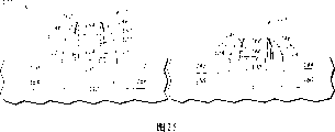
Shown in Figure 25 is to form with the device architecture 110 after forming silicide area 170,172,174 and 176 at silicide.Therefore, regions and source 142 and 144 is consumed by silicide regions 170,172,174 and 176 to a great extent.Equally, gate regions 114 and 116 is consumed a little by silicide area 164 and 168 respectively.This has stayed polysilicon segment 167 that is used for transistor 111 and the polysilicon segment 166 that is used for transistor 113.Although there is recess, source/drain part 178,180,182 and 184 is extended fully and is spread with covering gate polar region 167 and 166, although the recess that still has the removal by ARC to cause need overcome.The removal of this ARC is by wet etching, makes the amount (amount of therecess) of recess be starkly lower than dry etching.Though dry etching is preferred, under the situation of nonvolatile memory, overlapping fully conspicuousness is much larger than regular transistor.Therefore the more important thing is at floating grid with wherein have overlapping between the zone of charge storage, thereby in regions and source, to have well overlapping.And, by having after the formation of sidewall spacers 122 ARC that removes, the position of recess do not have with as Fig. 1-9 as shown in, under the situation of just removing ARC before this sidewall spacers of formation, seriously influence so.Under the situation of Fig. 1-9, after removing the ARC layer, formed sidewall spacers 24.
Claims (23)
1. method that forms integrated circuit (IC)-components on Semiconductor substrate comprises:
Form gate stack, this gate stack comprises grid on the gate-dielectric and the anti-reflection coating on this grid;
Form the first side wall at interval around grid, wherein this sidewall spacers comprises oxide;
On sidewall spacers and grid, form liner, and this liner on substrate from the sidewall spacers horizontal expansion;
Form second sidewall spacers around grid on liner, wherein this second sidewall spacers comprises nitride, and the part of this liner is between substrate and this second sidewall spacers; And
After forming second sidewall spacers, remove anti-reflection coating.
2. according to the method for claim 1, also be included in and form the source/drain injection of the first side wall interval execution afterwards to substrate.
3. according to the method for claim 2, wherein removing anti-reflection coating is wet processing.
4. according to the method for claim 2, wherein removing anti-reflection coating is dry process.
5. according to the method for claim 2, further comprise:
Be adjacent to second sidewall spacers and form the 3rd sidewall spacers, wherein the 3rd sidewall spacers is adjacent to second sidewall spacers.
6. according to the method for claim 5, wherein the 3rd sidewall spacers comprises oxide.
7. according to the method for claim 5, wherein source/drain injects and forms source/drain regions, further comprises:
On source/drain regions, form silicide regions.
8. according to the method for claim 7, wherein the 3rd sidewall spacers comprises amorphous silicon.
9. according to the process of claim 1 wherein that removing anti-reflection coating is wet processing.
10. according to the process of claim 1 wherein that this grid is the control grid, this lamination also comprises floating grid under this control grid and the insulating barrier between this control grid and this floating grid.
11. a method that forms integrated circuit (IC)-components comprises:
Semiconductor substrate is set;
On Semiconductor substrate, form the composition dielectric layer;
On the composition dielectric layer, form patterning conductive layer;
On patterning conductive layer, form anti-reflection coating;
On composition dielectric layer and patterning conductive layer, form first dielectric layer;
On first dielectric layer, form second dielectric layer;
On second dielectric layer, form ground floor;
Remove the part ground floor to form first patterned layer, wherein contiguous patterning conductive layer of first patterned layer and composition dielectric layer;
Remove part second dielectric to form first dielectric area of contiguous first patterned layer;
Remove part first dielectric to form second dielectric area of contiguous first dielectric area;
After removing this part first dielectric layer, remove anti-reflection coating;
Form the second layer on ground floor, wherein this second layer comprises amorphous silicon; And
Optionally remove a part of second layer at ground floor, thereby form the patterned first of contiguous first patterned layer in the second layer.
12. according to the method for claim 11, wherein removing anti-reflection coating is dry process.
13., further comprise and remove this part second layer according to the method for claim 11.
14. according to the method for claim 11, wherein first dielectric layer is an oxide, second dielectric layer is a nitride, and ground floor is an oxide.
15. according to the method for claim 14, wherein removing anti-reflection coating is wet processing.
16. a method that forms integrated circuit (IC)-components comprises:
Setting has the Semiconductor substrate of first and second portion;
Form gate stack, this gate stack comprises:
The gate-dielectric that in the first of Semiconductor substrate, forms; With
The gate electrode that on gate-dielectric, forms;
On gate stack, form the first composition anti-reflection coating;
Form the nonvolatile memory lamination, this lamination comprises:
The charge storage layer that on the second portion of Semiconductor substrate, forms; With
First dielectric layer that on charge storage layer, forms;
On the nonvolatile memory lamination, form the second composition anti-reflection coating;
On gate stack and nonvolatile memory lamination, form second dielectric layer;
Remove part second dielectric layer to form first interval of adjacent gate lamination and nonvolatile memory lamination;
After removing part second dielectric layer, remove the first composition anti-reflection coating and the second composition anti-reflection coating;
Below gate stack, form first raceway groove; With
Below the nonvolatile memory lamination, form second raceway groove.
17. the method according to claim 16 also comprises:
On first interval, form the 3rd dielectric layer;
On the 3rd dielectric layer, form the 4th dielectric layer;
Remove part the 3rd dielectric layer to form second interval at contiguous first interval; With
Remove part the 4th dielectric layer to form the 3rd interval at contiguous second interval.
18., wherein remove the first composition anti-reflection coating and the second composition anti-reflection coating and before forming the 3rd dielectric layer and forming the 4th dielectric layer, carry out according to the method for claim 17.
19. according to the method for claim 18, wherein make the second dielectric layer densification before at interval forming first, and remove the first composition anti-reflection coating and the second composition anti-reflection coating is a wet processing.
20. according to the method for claim 19, wherein second dielectric layer is an oxide, the 3rd dielectric layer is an oxide, and the 4th dielectric layer is a nitride.
21. an integrated circuit (IC)-components comprises:
Semiconductor substrate;
Lamination comprises:
The composition dielectric layer that on Semiconductor substrate, forms;
The patterning conductive layer that on the composition dielectric layer, forms;
The first side wall; With
Second sidewall, wherein second sidewall is relative with the first side wall;
The first region at the inner and contiguous the first side wall of Semiconductor substrate;
Second electrode district at inner and contiguous second sidewall of Semiconductor substrate;
Channel region between the first region and second electrode district and below lamination;
The oxide spacer of the contiguous the first side wall and second sidewall, wherein oxide spacer has first height on the top surface of Semiconductor substrate;
The nitride spacers of contiguous first oxide spacer, wherein nitride spacers has second height on the top surface of Semiconductor substrate, that be lower than first height; And
Between oxide spacer and the nitride spacers and the insulating barrier on first and second electrode districts;
Wherein this substrate have with oxide spacer and insulating barrier between the recess that aligns of interface.
22. an integrated circuit (IC)-components comprises:
Semiconductor substrate with top surface;
The lamination that on Semiconductor substrate, forms, this lamination comprises:
Ground floor;
The second layer that on ground floor, forms;
The first side wall; With
Second sidewall relative with the first side wall;
Interval in abutting connection with the first side wall and second sidewall, under wherein the first of the top surface of Semiconductor substrate was positioned at interval, second portion was positioned under the lamination, first basically with the second portion coplane, this has bottom, this bottom whole on the first of Semiconductor substrate at interval;
The uniform basically insulating barrier of thickness, its first's adjacent partition, and second portion is directly on the third part of the top surface of Semiconductor substrate, and wherein the third part of the top surface of this Semiconductor substrate falls in respect to the first and the second portion of substrate;
First doped region at the inner and contiguous the first side wall of Semiconductor substrate;
Second doped region at inner and contiguous second sidewall of Semiconductor substrate; With
Between first doped region and second doped region and at the channel region of Semiconductor substrate inside.
23. according to the integrated circuit (IC)-components of claim 22, wherein the second portion of the first of first doped region and second doped region is positioned under the ground floor.
Applications Claiming Priority (2)
| Application Number | Priority Date | Filing Date | Title |
|---|---|---|---|
| US10/101,298 | 2002-03-19 | ||
| US10/101,298 US6753242B2 (en) | 2002-03-19 | 2002-03-19 | Integrated circuit device and method therefor |
Publications (2)
| Publication Number | Publication Date |
|---|---|
| CN1643671A CN1643671A (en) | 2005-07-20 |
| CN100339961C true CN100339961C (en) | 2007-09-26 |
Family
ID=28039985
Family Applications (1)
| Application Number | Title | Priority Date | Filing Date |
|---|---|---|---|
| CNB038062992A Expired - Fee Related CN100339961C (en) | 2002-03-19 | 2003-03-14 | Integrated circuit device and method therefor |
Country Status (8)
| Country | Link |
|---|---|
| US (2) | US6753242B2 (en) |
| EP (1) | EP1485948A1 (en) |
| JP (1) | JP2005531919A (en) |
| KR (1) | KR100961404B1 (en) |
| CN (1) | CN100339961C (en) |
| AU (1) | AU2003225792A1 (en) |
| TW (1) | TWI283029B (en) |
| WO (1) | WO2003081660A1 (en) |
Cited By (2)
| Publication number | Priority date | Publication date | Assignee | Title |
|---|---|---|---|---|
| CN104752223A (en) * | 2013-12-31 | 2015-07-01 | 中芯国际集成电路制造(上海)有限公司 | Semiconductor device and forming method thereof |
| CN106653847A (en) * | 2015-10-28 | 2017-05-10 | 台湾积体电路制造股份有限公司 | Method for fabricating self-aligned contact in a semiconductor device |
Families Citing this family (25)
| Publication number | Priority date | Publication date | Assignee | Title |
|---|---|---|---|---|
| KR100488099B1 (en) * | 2002-11-18 | 2005-05-06 | 한국전자통신연구원 | A mos transistor having short channel and a manufacturing method thereof |
| US6884712B2 (en) * | 2003-02-07 | 2005-04-26 | Chartered Semiconductor Manufacturing, Ltd. | Method of manufacturing semiconductor local interconnect and contact |
| US6913980B2 (en) * | 2003-06-30 | 2005-07-05 | Texas Instruments Incorporated | Process method of source drain spacer engineering to improve transistor capacitance |
| JP2005109381A (en) * | 2003-10-02 | 2005-04-21 | Oki Electric Ind Co Ltd | Manufacturing method for semiconductor device |
| US7064027B2 (en) * | 2003-11-13 | 2006-06-20 | International Business Machines Corporation | Method and structure to use an etch resistant liner on transistor gate structure to achieve high device performance |
| US7229885B2 (en) * | 2004-01-06 | 2007-06-12 | International Business Machines Corporation | Formation of a disposable spacer to post dope a gate conductor |
| US7064396B2 (en) * | 2004-03-01 | 2006-06-20 | Freescale Semiconductor, Inc. | Integrated circuit with multiple spacer insulating region widths |
| US8896048B1 (en) * | 2004-06-04 | 2014-11-25 | Spansion Llc | Apparatus and method for source side implantation after spacer formation to reduce short channel effects in metal oxide semiconductor field effect transistors |
| KR100541657B1 (en) * | 2004-06-29 | 2006-01-11 | 삼성전자주식회사 | Multi-gate transistor fabrication method and multi-gate transistor fabricated thereby |
| US7170130B2 (en) * | 2004-08-11 | 2007-01-30 | Spansion Llc | Memory cell with reduced DIBL and Vss resistance |
| KR100668954B1 (en) * | 2004-12-15 | 2007-01-12 | 동부일렉트로닉스 주식회사 | Method for manufacturing of the thin film transistor |
| KR100685575B1 (en) * | 2004-12-28 | 2007-02-22 | 주식회사 하이닉스반도체 | Method for forming step channel of semiconductor device |
| US7544553B2 (en) * | 2005-03-30 | 2009-06-09 | Infineon Technologies Ag | Integration scheme for fully silicided gate |
| US20070007578A1 (en) * | 2005-07-07 | 2007-01-11 | Li Chi N B | Sub zero spacer for shallow MDD junction to improve BVDSS in NVM bitcell |
| US8159030B2 (en) * | 2005-11-30 | 2012-04-17 | Globalfoundries Inc. | Strained MOS device and methods for its fabrication |
| KR100741908B1 (en) * | 2005-12-30 | 2007-07-24 | 동부일렉트로닉스 주식회사 | Method of fabricating semiconductor device |
| US7317222B2 (en) * | 2006-01-27 | 2008-01-08 | Freescale Semiconductor, Inc. | Memory cell using a dielectric having non-uniform thickness |
| JP4799217B2 (en) * | 2006-03-03 | 2011-10-26 | Okiセミコンダクタ株式会社 | Manufacturing method of semiconductor device |
| JP2008098567A (en) * | 2006-10-16 | 2008-04-24 | Toshiba Corp | Nonvolatile semiconductor memory, and its manufacturing method |
| US7745344B2 (en) * | 2007-10-29 | 2010-06-29 | Freescale Semiconductor, Inc. | Method for integrating NVM circuitry with logic circuitry |
| KR101815527B1 (en) | 2010-10-07 | 2018-01-05 | 삼성전자주식회사 | Semiconductor device and method for manufacturing the same |
| CN102420116B (en) * | 2011-06-07 | 2013-12-04 | 上海华力微电子有限公司 | Method for eliminating recess defect of gate electrode |
| JP5715551B2 (en) * | 2011-11-25 | 2015-05-07 | 株式会社東芝 | Semiconductor device and manufacturing method thereof |
| US9941388B2 (en) * | 2014-06-19 | 2018-04-10 | Globalfoundries Inc. | Method and structure for protecting gates during epitaxial growth |
| US11653498B2 (en) * | 2017-11-30 | 2023-05-16 | Taiwan Semiconductor Manufacturing Co., Ltd. | Memory device with improved data retention |
Citations (4)
| Publication number | Priority date | Publication date | Assignee | Title |
|---|---|---|---|---|
| US5902125A (en) * | 1997-12-29 | 1999-05-11 | Texas Instruments--Acer Incorporated | Method to form stacked-Si gate pMOSFETs with elevated and extended S/D junction |
| US5972762A (en) * | 1998-01-05 | 1999-10-26 | Texas Instruments--Acer Incorporated | Method of forming mosfets with recessed self-aligned silicide gradual S/D junction |
| US6066567A (en) * | 1997-12-18 | 2000-05-23 | Advanced Micro Devices, Inc. | Methods for in-situ removal of an anti-reflective coating during an oxide resistor protect etching process |
| US6087271A (en) * | 1997-12-18 | 2000-07-11 | Advanced Micro Devices, Inc. | Methods for removal of an anti-reflective coating following a resist protect etching process |
Family Cites Families (10)
| Publication number | Priority date | Publication date | Assignee | Title |
|---|---|---|---|---|
| US5960270A (en) * | 1997-08-11 | 1999-09-28 | Motorola, Inc. | Method for forming an MOS transistor having a metallic gate electrode that is formed after the formation of self-aligned source and drain regions |
| US6245682B1 (en) | 1999-03-11 | 2001-06-12 | Taiwan Semiconductor Manufacturing Company | Removal of SiON ARC film after poly photo and etch |
| US6271133B1 (en) * | 1999-04-12 | 2001-08-07 | Chartered Semiconductor Manufacturing Ltd. | Optimized Co/Ti-salicide scheme for shallow junction deep sub-micron device fabrication |
| EP1188179A2 (en) | 1999-12-30 | 2002-03-20 | Koninklijke Philips Electronics N.V. | An improved method for buried anti-reflective coating removal |
| US6156126A (en) | 2000-01-18 | 2000-12-05 | United Microelectronics Corp. | Method for reducing or avoiding the formation of a silicon recess in SDE junction regions |
| US6372589B1 (en) * | 2000-04-19 | 2002-04-16 | Advanced Micro Devices, Inc. | Method of forming ultra-shallow source/drain extension by impurity diffusion from doped dielectric spacer |
| US6368947B1 (en) * | 2000-06-20 | 2002-04-09 | Advanced Micro Devices, Inc. | Process utilizing a cap layer optimized to reduce gate line over-melt |
| US6555865B2 (en) * | 2001-07-10 | 2003-04-29 | Samsung Electronics Co. Ltd. | Nonvolatile semiconductor memory device with a multi-layer sidewall spacer structure and method for manufacturing the same |
| US6818504B2 (en) * | 2001-08-10 | 2004-11-16 | Hynix Semiconductor America, Inc. | Processes and structures for self-aligned contact non-volatile memory with peripheral transistors easily modifiable for various technologies and applications |
| US6812515B2 (en) * | 2001-11-26 | 2004-11-02 | Hynix Semiconductor, Inc. | Polysilicon layers structure and method of forming same |
-
2002
- 2002-03-19 US US10/101,298 patent/US6753242B2/en not_active Expired - Lifetime
-
2003
- 2003-03-14 WO PCT/US2003/007835 patent/WO2003081660A1/en active Application Filing
- 2003-03-14 KR KR1020047014786A patent/KR100961404B1/en not_active IP Right Cessation
- 2003-03-14 JP JP2003579272A patent/JP2005531919A/en active Pending
- 2003-03-14 AU AU2003225792A patent/AU2003225792A1/en not_active Abandoned
- 2003-03-14 EP EP03745106A patent/EP1485948A1/en not_active Withdrawn
- 2003-03-14 CN CNB038062992A patent/CN100339961C/en not_active Expired - Fee Related
- 2003-03-18 TW TW092105907A patent/TWI283029B/en not_active IP Right Cessation
- 2003-12-16 US US10/737,116 patent/US6846716B2/en not_active Expired - Lifetime
Patent Citations (4)
| Publication number | Priority date | Publication date | Assignee | Title |
|---|---|---|---|---|
| US6066567A (en) * | 1997-12-18 | 2000-05-23 | Advanced Micro Devices, Inc. | Methods for in-situ removal of an anti-reflective coating during an oxide resistor protect etching process |
| US6087271A (en) * | 1997-12-18 | 2000-07-11 | Advanced Micro Devices, Inc. | Methods for removal of an anti-reflective coating following a resist protect etching process |
| US5902125A (en) * | 1997-12-29 | 1999-05-11 | Texas Instruments--Acer Incorporated | Method to form stacked-Si gate pMOSFETs with elevated and extended S/D junction |
| US5972762A (en) * | 1998-01-05 | 1999-10-26 | Texas Instruments--Acer Incorporated | Method of forming mosfets with recessed self-aligned silicide gradual S/D junction |
Cited By (4)
| Publication number | Priority date | Publication date | Assignee | Title |
|---|---|---|---|---|
| CN104752223A (en) * | 2013-12-31 | 2015-07-01 | 中芯国际集成电路制造(上海)有限公司 | Semiconductor device and forming method thereof |
| CN104752223B (en) * | 2013-12-31 | 2017-12-29 | 中芯国际集成电路制造(上海)有限公司 | Semiconductor devices and forming method thereof |
| CN106653847A (en) * | 2015-10-28 | 2017-05-10 | 台湾积体电路制造股份有限公司 | Method for fabricating self-aligned contact in a semiconductor device |
| CN106653847B (en) * | 2015-10-28 | 2020-07-17 | 台湾积体电路制造股份有限公司 | Method of manufacturing self-aligned contact in semiconductor device |
Also Published As
| Publication number | Publication date |
|---|---|
| US6846716B2 (en) | 2005-01-25 |
| AU2003225792A1 (en) | 2003-10-08 |
| TW200305954A (en) | 2003-11-01 |
| EP1485948A1 (en) | 2004-12-15 |
| US6753242B2 (en) | 2004-06-22 |
| US20030181028A1 (en) | 2003-09-25 |
| US20040124450A1 (en) | 2004-07-01 |
| TWI283029B (en) | 2007-06-21 |
| WO2003081660A1 (en) | 2003-10-02 |
| JP2005531919A (en) | 2005-10-20 |
| KR20040097188A (en) | 2004-11-17 |
| KR100961404B1 (en) | 2010-06-09 |
| CN1643671A (en) | 2005-07-20 |
Similar Documents
| Publication | Publication Date | Title |
|---|---|---|
| CN100339961C (en) | Integrated circuit device and method therefor | |
| KR100487532B1 (en) | Flash memory devices having shallow trench isolation structures and methods of fabricating the same | |
| US6768161B2 (en) | Semiconductor device having floating gate and method of producing the same | |
| KR100206985B1 (en) | Flash memory device and fabrication method of the same | |
| JP2000150678A (en) | Nonvolatile semiconductor memory and fabrication thereof | |
| KR100230814B1 (en) | Flash memory device and its manufacturing method | |
| US6391717B1 (en) | Method of manufacturing a flash memory device | |
| US20070004099A1 (en) | NAND flash memory device and method of manufacturing the same | |
| JP2008010817A (en) | Manufacturing method of nand flash memory device | |
| US20050156229A1 (en) | Integrated circuit device and method therefor | |
| KR100199370B1 (en) | Method of manufacturing the flash memory cell | |
| KR100301244B1 (en) | Method of forming a flash memory device | |
| KR20060074177A (en) | Method of manufacturing a flash memory device | |
| KR100187679B1 (en) | Method of making flash memory cell | |
| US6365449B1 (en) | Process for making a non-volatile memory cell with a polysilicon spacer defined select gate | |
| US20070181916A1 (en) | Method of manufacturing flash memory device | |
| KR100339420B1 (en) | Method for fabricating semiconductor memory device | |
| US7560770B2 (en) | MOSFET device suppressing electrical coupling between adjoining recess gates and method for manufacturing the same | |
| KR100719738B1 (en) | Flash memory device and method of operating and manufacturing the same | |
| KR19980053442A (en) | Flash memory cell manufacturing method | |
| KR100654558B1 (en) | Method for forming floating gate in flash memory device | |
| KR100908545B1 (en) | Method of manufacturing semiconductor device | |
| JP2985845B2 (en) | Semiconductor device and manufacturing method thereof | |
| CN111261706A (en) | Memory structure and manufacturing method thereof | |
| KR20020096741A (en) | Method of manufacturing a flash memory cell |
Legal Events
| Date | Code | Title | Description |
|---|---|---|---|
| C06 | Publication | ||
| PB01 | Publication | ||
| C10 | Entry into substantive examination | ||
| SE01 | Entry into force of request for substantive examination | ||
| C14 | Grant of patent or utility model | ||
| GR01 | Patent grant | ||
| CP01 | Change in the name or title of a patent holder |
Address after: Texas in the United States Patentee after: NXP America Co Ltd Address before: Texas in the United States Patentee before: Fisical Semiconductor Inc. |
|
| CP01 | Change in the name or title of a patent holder | ||
| CF01 | Termination of patent right due to non-payment of annual fee |
Granted publication date: 20070926 Termination date: 20190314 |
|
| CF01 | Termination of patent right due to non-payment of annual fee |