KR102017360B1 - Nonpolymeric antireflection compositions containing adamantyl groups - Google Patents
Nonpolymeric antireflection compositions containing adamantyl groups Download PDFInfo
- Publication number
- KR102017360B1 KR102017360B1 KR1020147021741A KR20147021741A KR102017360B1 KR 102017360 B1 KR102017360 B1 KR 102017360B1 KR 1020147021741 A KR1020147021741 A KR 1020147021741A KR 20147021741 A KR20147021741 A KR 20147021741A KR 102017360 B1 KR102017360 B1 KR 102017360B1
- Authority
- KR
- South Korea
- Prior art keywords
- group
- layer
- compound
- independently
- antireflective
- Prior art date
Links
Images


Classifications
-
- C—CHEMISTRY; METALLURGY
- C09—DYES; PAINTS; POLISHES; NATURAL RESINS; ADHESIVES; COMPOSITIONS NOT OTHERWISE PROVIDED FOR; APPLICATIONS OF MATERIALS NOT OTHERWISE PROVIDED FOR
- C09D—COATING COMPOSITIONS, e.g. PAINTS, VARNISHES OR LACQUERS; FILLING PASTES; CHEMICAL PAINT OR INK REMOVERS; INKS; CORRECTING FLUIDS; WOODSTAINS; PASTES OR SOLIDS FOR COLOURING OR PRINTING; USE OF MATERIALS THEREFOR
- C09D5/00—Coating compositions, e.g. paints, varnishes or lacquers, characterised by their physical nature or the effects produced; Filling pastes
- C09D5/006—Anti-reflective coatings
-
- C—CHEMISTRY; METALLURGY
- C07—ORGANIC CHEMISTRY
- C07C—ACYCLIC OR CARBOCYCLIC COMPOUNDS
- C07C69/00—Esters of carboxylic acids; Esters of carbonic or haloformic acids
- C07C69/76—Esters of carboxylic acids having a carboxyl group bound to a carbon atom of a six-membered aromatic ring
-
- C—CHEMISTRY; METALLURGY
- C07—ORGANIC CHEMISTRY
- C07C—ACYCLIC OR CARBOCYCLIC COMPOUNDS
- C07C69/00—Esters of carboxylic acids; Esters of carbonic or haloformic acids
- C07C69/76—Esters of carboxylic acids having a carboxyl group bound to a carbon atom of a six-membered aromatic ring
- C07C69/94—Esters of carboxylic acids having a carboxyl group bound to a carbon atom of a six-membered aromatic ring of polycyclic hydroxy carboxylic acids, the hydroxy groups and the carboxyl groups of which are bound to carbon atoms of six-membered aromatic rings
-
- C—CHEMISTRY; METALLURGY
- C07—ORGANIC CHEMISTRY
- C07D—HETEROCYCLIC COMPOUNDS
- C07D303/00—Compounds containing three-membered rings having one oxygen atom as the only ring hetero atom
- C07D303/02—Compounds containing oxirane rings
- C07D303/12—Compounds containing oxirane rings with hydrocarbon radicals, substituted by singly or doubly bound oxygen atoms
- C07D303/18—Compounds containing oxirane rings with hydrocarbon radicals, substituted by singly or doubly bound oxygen atoms by etherified hydroxyl radicals
- C07D303/20—Ethers with hydroxy compounds containing no oxirane rings
- C07D303/22—Ethers with hydroxy compounds containing no oxirane rings with monohydroxy compounds
- C07D303/23—Oxiranylmethyl ethers of compounds having one hydroxy group bound to a six-membered aromatic ring, the oxiranylmethyl radical not being further substituted, i.e.
-
- G—PHYSICS
- G03—PHOTOGRAPHY; CINEMATOGRAPHY; ANALOGOUS TECHNIQUES USING WAVES OTHER THAN OPTICAL WAVES; ELECTROGRAPHY; HOLOGRAPHY
- G03F—PHOTOMECHANICAL PRODUCTION OF TEXTURED OR PATTERNED SURFACES, e.g. FOR PRINTING, FOR PROCESSING OF SEMICONDUCTOR DEVICES; MATERIALS THEREFOR; ORIGINALS THEREFOR; APPARATUS SPECIALLY ADAPTED THEREFOR
- G03F7/00—Photomechanical, e.g. photolithographic, production of textured or patterned surfaces, e.g. printing surfaces; Materials therefor, e.g. comprising photoresists; Apparatus specially adapted therefor
- G03F7/004—Photosensitive materials
- G03F7/09—Photosensitive materials characterised by structural details, e.g. supports, auxiliary layers
- G03F7/091—Photosensitive materials characterised by structural details, e.g. supports, auxiliary layers characterised by antireflection means or light filtering or absorbing means, e.g. anti-halation, contrast enhancement
-
- G—PHYSICS
- G03—PHOTOGRAPHY; CINEMATOGRAPHY; ANALOGOUS TECHNIQUES USING WAVES OTHER THAN OPTICAL WAVES; ELECTROGRAPHY; HOLOGRAPHY
- G03F—PHOTOMECHANICAL PRODUCTION OF TEXTURED OR PATTERNED SURFACES, e.g. FOR PRINTING, FOR PROCESSING OF SEMICONDUCTOR DEVICES; MATERIALS THEREFOR; ORIGINALS THEREFOR; APPARATUS SPECIALLY ADAPTED THEREFOR
- G03F7/00—Photomechanical, e.g. photolithographic, production of textured or patterned surfaces, e.g. printing surfaces; Materials therefor, e.g. comprising photoresists; Apparatus specially adapted therefor
- G03F7/004—Photosensitive materials
- G03F7/09—Photosensitive materials characterised by structural details, e.g. supports, auxiliary layers
- G03F7/094—Multilayer resist systems, e.g. planarising layers
-
- G—PHYSICS
- G03—PHOTOGRAPHY; CINEMATOGRAPHY; ANALOGOUS TECHNIQUES USING WAVES OTHER THAN OPTICAL WAVES; ELECTROGRAPHY; HOLOGRAPHY
- G03F—PHOTOMECHANICAL PRODUCTION OF TEXTURED OR PATTERNED SURFACES, e.g. FOR PRINTING, FOR PROCESSING OF SEMICONDUCTOR DEVICES; MATERIALS THEREFOR; ORIGINALS THEREFOR; APPARATUS SPECIALLY ADAPTED THEREFOR
- G03F7/00—Photomechanical, e.g. photolithographic, production of textured or patterned surfaces, e.g. printing surfaces; Materials therefor, e.g. comprising photoresists; Apparatus specially adapted therefor
- G03F7/26—Processing photosensitive materials; Apparatus therefor
- G03F7/30—Imagewise removal using liquid means
-
- G—PHYSICS
- G03—PHOTOGRAPHY; CINEMATOGRAPHY; ANALOGOUS TECHNIQUES USING WAVES OTHER THAN OPTICAL WAVES; ELECTROGRAPHY; HOLOGRAPHY
- G03F—PHOTOMECHANICAL PRODUCTION OF TEXTURED OR PATTERNED SURFACES, e.g. FOR PRINTING, FOR PROCESSING OF SEMICONDUCTOR DEVICES; MATERIALS THEREFOR; ORIGINALS THEREFOR; APPARATUS SPECIALLY ADAPTED THEREFOR
- G03F7/00—Photomechanical, e.g. photolithographic, production of textured or patterned surfaces, e.g. printing surfaces; Materials therefor, e.g. comprising photoresists; Apparatus specially adapted therefor
- G03F7/26—Processing photosensitive materials; Apparatus therefor
- G03F7/40—Treatment after imagewise removal, e.g. baking
-
- C—CHEMISTRY; METALLURGY
- C07—ORGANIC CHEMISTRY
- C07C—ACYCLIC OR CARBOCYCLIC COMPOUNDS
- C07C2603/00—Systems containing at least three condensed rings
- C07C2603/02—Ortho- or ortho- and peri-condensed systems
- C07C2603/04—Ortho- or ortho- and peri-condensed systems containing three rings
- C07C2603/22—Ortho- or ortho- and peri-condensed systems containing three rings containing only six-membered rings
- C07C2603/24—Anthracenes; Hydrogenated anthracenes
-
- C—CHEMISTRY; METALLURGY
- C07—ORGANIC CHEMISTRY
- C07C—ACYCLIC OR CARBOCYCLIC COMPOUNDS
- C07C2603/00—Systems containing at least three condensed rings
- C07C2603/56—Ring systems containing bridged rings
- C07C2603/58—Ring systems containing bridged rings containing three rings
- C07C2603/70—Ring systems containing bridged rings containing three rings containing only six-membered rings
- C07C2603/74—Adamantanes
-
- H—ELECTRICITY
- H01—ELECTRIC ELEMENTS
- H01L—SEMICONDUCTOR DEVICES NOT COVERED BY CLASS H10
- H01L21/00—Processes or apparatus adapted for the manufacture or treatment of semiconductor or solid state devices or of parts thereof
- H01L21/02—Manufacture or treatment of semiconductor devices or of parts thereof
- H01L21/027—Making masks on semiconductor bodies for further photolithographic processing not provided for in group H01L21/18 or H01L21/34
- H01L21/0271—Making masks on semiconductor bodies for further photolithographic processing not provided for in group H01L21/18 or H01L21/34 comprising organic layers
- H01L21/0273—Making masks on semiconductor bodies for further photolithographic processing not provided for in group H01L21/18 or H01L21/34 comprising organic layers characterised by the treatment of photoresist layers
- H01L21/0274—Photolithographic processes
- H01L21/0276—Photolithographic processes using an anti-reflective coating
-
- Y—GENERAL TAGGING OF NEW TECHNOLOGICAL DEVELOPMENTS; GENERAL TAGGING OF CROSS-SECTIONAL TECHNOLOGIES SPANNING OVER SEVERAL SECTIONS OF THE IPC; TECHNICAL SUBJECTS COVERED BY FORMER USPC CROSS-REFERENCE ART COLLECTIONS [XRACs] AND DIGESTS
- Y10—TECHNICAL SUBJECTS COVERED BY FORMER USPC
- Y10T—TECHNICAL SUBJECTS COVERED BY FORMER US CLASSIFICATION
- Y10T428/00—Stock material or miscellaneous articles
- Y10T428/26—Web or sheet containing structurally defined element or component, the element or component having a specified physical dimension
- Y10T428/263—Coating layer not in excess of 5 mils thick or equivalent
- Y10T428/264—Up to 3 mils
- Y10T428/265—1 mil or less
-
- Y—GENERAL TAGGING OF NEW TECHNOLOGICAL DEVELOPMENTS; GENERAL TAGGING OF CROSS-SECTIONAL TECHNOLOGIES SPANNING OVER SEVERAL SECTIONS OF THE IPC; TECHNICAL SUBJECTS COVERED BY FORMER USPC CROSS-REFERENCE ART COLLECTIONS [XRACs] AND DIGESTS
- Y10—TECHNICAL SUBJECTS COVERED BY FORMER USPC
- Y10T—TECHNICAL SUBJECTS COVERED BY FORMER US CLASSIFICATION
- Y10T428/00—Stock material or miscellaneous articles
- Y10T428/31504—Composite [nonstructural laminate]
- Y10T428/31511—Of epoxy ether
- Y10T428/31525—Next to glass or quartz
-
- Y—GENERAL TAGGING OF NEW TECHNOLOGICAL DEVELOPMENTS; GENERAL TAGGING OF CROSS-SECTIONAL TECHNOLOGIES SPANNING OVER SEVERAL SECTIONS OF THE IPC; TECHNICAL SUBJECTS COVERED BY FORMER USPC CROSS-REFERENCE ART COLLECTIONS [XRACs] AND DIGESTS
- Y10—TECHNICAL SUBJECTS COVERED BY FORMER USPC
- Y10T—TECHNICAL SUBJECTS COVERED BY FORMER US CLASSIFICATION
- Y10T428/00—Stock material or miscellaneous articles
- Y10T428/31504—Composite [nonstructural laminate]
- Y10T428/31511—Of epoxy ether
- Y10T428/31529—Next to metal
Abstract
본 발명은 비폴리머성 화합물, 조성물, 및 마이크로 전자 형성방법, 및 그로부터 형성된 구조에 관한 것이다. 비폴리머성 화합물은 고리-열린, 에폭사이드-아다만탄 유도체이며, 발색단과 같이 하나 이상의 화학적 개질기와 함께, 각각의 에폭시 잔기에 결합하는 둘 이상의 에폭시 잔기 및 하나 이상의 아다만틸 기를 포함한다. 반사 방지 및/또는 평탄화 조성물이 상기 조성물을 사용하여 형성될 수 있으며, 마이크로 전자 구조의 제조를 포함하여, 리소그래피 공정에서 사용될 수 있다. The present invention relates to nonpolymeric compounds, compositions, and methods for forming microelectronics, and structures formed therefrom. Non-polymeric compounds are ring-opened, epoxide-adamantane derivatives and comprise two or more epoxy residues and one or more adamantyl groups that bind to each epoxy residue, along with one or more chemical modifiers, such as chromophores. Antireflective and / or planarizing compositions may be formed using the compositions and used in lithographic processes, including the manufacture of microelectronic structures.
Description
관련 출원의 상호 참조Cross Reference of Related Application
본 출원은 “아다만틸 기를 포함하는 비폴리머성 반사 방지 조성물”이란 명칭으로 2012년 1월 19일에 출원된 미국 가특허 출원 제61/588,268호를 우선권으로 주장하며, 이 출원은 전부 본 명세서에 참고로서 포함된다.
This application claims priority to US Provisional Patent Application No. 61 / 588,268, filed Jan. 19, 2012, entitled “Non-Polymeric Anti-Reflective Composition Containing Adamantyl Group,” which is incorporated herein by reference in its entirety. Included as a reference.
기술분야Field of technology
본 발명은 마이크로 전자 제작 공정을 포함하여, 리소그래피(lithography) 공정에서 반사 방지(anti-reflective) 코팅 및/또는 평탄화 층(planarization layer)으로서 유용한 비폴리머성 아다만틸(nonpolymeric adamantyl) 화합물을 포함하는 조성물에 관한 것이다. The invention includes nonpolymeric adamantyl compounds useful as anti-reflective coatings and / or planarization layers in lithography processes, including microelectronic fabrication processes. It relates to a composition.
집적 회로 제조업자들은 수율을 향상시키고 단위 비용을 절감하며, 온-칩(on-chip) 컴퓨팅 파워(computing power)를 증가시키기 위하여, 웨이퍼 크기를 최대화하고 장치 피처 치수(feature dimension)를 최소화하는 것을 지속적으로 추구하고 있다. 리소그래피 기술의 향상 및 더 작은-파장의 포토리소그래피 방사선원(radiation source)은 현재 20nm 가까운 피처의 생산을 가능하도록 해준다. 포토래지스트 노광(exposure) 동안에 기판 반사율을 감소 및/또는 최대화하는 것은 상기 작은 피처의 치수 조절을 유지하는데 있어 중요하다. 따라서, 반사 방지 코팅으로 알려진 광 흡수성 유기 폴리머는 포토래지스트 노광 동안에 반도체 기판과 통상적으로 접하는 반사율을 감소시키기 위하여, 포토래지스트층 아래에 도포된다.
Integrated circuit manufacturers are seeking to maximize wafer size and minimize device feature dimensions in order to improve yield, reduce unit cost, and increase on-chip computing power. We are constantly pursuing. Improvements in lithography technology and smaller-wavelength photolithography radiation sources now enable the production of features close to 20 nm. Reducing and / or maximizing substrate reflectance during photoresist exposure is important in maintaining dimensional control of the small feature. Thus, a light absorbing organic polymer known as an antireflective coating is applied under the photoresist layer in order to reduce the reflectivity typically encountered with the semiconductor substrate during photoresist exposure.
종래 기술의 반사 방지 코팅층은 수지와 블렌드되거나 수지에 부착되는 광-흡수성 발색단(chromophore)을 가진 폴리머성 수지를 포함한다. 높은 광학도(optical density)는 상기 폴리머들이 효과적인 반사율 조절을 제공할 수 있도록 함에도 불구하고, 또한 다양한 문제점들을 갖는다. 예를 들어, 상기 폴리머들은 폴리머 블렌딩(blending)하는 동안에 문제를 야기하는 높은 분자량을 갖는다. 보다 구체적으로, 상기 폴리머의 사용은 특수한 포토리소그래피 공정에서 사용되는 포토래지스트에 대한 반사 방지 코팅의 주문제작(customization)을 방해한다. 주문제작은 반사 방지 코팅에 대한 포토래지스트의 보다 우수한 접착 및 보다 직선 프로파일(straighter profile)을 가능하게 하여서, 보다 우수한 성능을 나타내기 때문에 특히 중요하다. 더 작은 분자량 구성요소는 또한 보다 우수한 유동 특성을 가능하게 하며, 장치 표면에 토포그래피(topography)를 채울 수 있는 물질의 능력을 증가시키며, 포토래지스트 도포(application)용으로 보다 평면상 표면을 만든다. 따라서, 당해 기술분야에서 향상된 반사 방지 또는 평탄화 코팅 조성물에 대한 요구가 존재한다. Prior art antireflective coatings include polymeric resins having light-absorbing chromophores that blend with or adhere to the resin. Although high optical density allows the polymers to provide effective reflectance control, they also have various problems. For example, the polymers have a high molecular weight which causes problems during polymer blending. More specifically, the use of such polymers hinders the customization of antireflective coatings for photoresists used in special photolithography processes. Customization is particularly important because it allows for better adhesion of the photoresist to the antireflective coating and a more straighter profile, resulting in better performance. Smaller molecular weight components also allow for better flow properties, increase the ability of the material to fill the topography of the device surface, and create a more planar surface for photoresist applications. . Thus, there is a need in the art for improved antireflective or planarized coating compositions.
발명의 간단한 설명Brief Description of the Invention
본 명세서에 개시되는 발명은 대락적으로 마이크로 전자 구조를 형성하기 위한 화합물, 조성물 및 방법과 그로부터 형성되는 구조에 관한 것이다. 하나 이상의 실시형태에서, 본 발명은 마이크로 전자 구조 형성용 방법은 표면을 가진 마이크로 전자 기판을 제공하는 단계; 선택적으로 상기 기판 표면에 하나 이상의 중간 하지층(intermediate underlayer)을 형성하는 단계; 및 중간 하지층이 존재하는 경우에는 상기 중간 하지층에 인접한, 또는 중간 하지층이 존재하지 않는 경우에는 상기 기판 표면에 인접한 반사 방지층 또는 평탄화 층을 형성하는 단계를 포함한다. 상기 반사 방지층 또는 평탄화 층은 용매 계에서 분산되거나 용해된 비폴리머성 화합물을 포함하는 조성물로부터 형성된다. 상기 비폴리머성 화합물은 둘 이상의 에폭시 잔기(moiety) 및 하나 이상의 아다만틸 기를 포함한다.
The invention disclosed herein broadly relates to compounds, compositions and methods for forming microelectronic structures and structures formed therefrom. In one or more embodiments, the present invention provides a method for forming a microelectronic structure comprising providing a microelectronic substrate having a surface; Optionally forming at least one intermediate underlayer on the substrate surface; And forming an antireflective layer or planarization layer adjacent to the intermediate underlayer if present, or adjacent to the substrate surface if no intermediate underlayer is present. The antireflection layer or planarization layer is formed from a composition comprising a nonpolymeric compound dispersed or dissolved in a solvent system. The nonpolymeric compound comprises two or more epoxy moieties and one or more adamantyl groups.
본 명세서는 또한 마이크로 전자 구조 형성에 유용한 반사 방지 또는 평탄화 조성물을 개시한다. 상기 조성물은 용매 계에 분산되거나 용해된 비폴리머성 화합물을 포함한다. 비폴리머성 화합물은 둘 이상의 에폭시 잔기 및 하나 이상의 아다만틸 기를 포함하며, 여기서 상기 에폭시 잔기의 하나 이상은 화학적 개질기(modification group)를 포함한다.
The present disclosure also discloses antireflective or planarizing compositions useful for forming microelectronic structures. The composition comprises a nonpolymeric compound dispersed or dissolved in a solvent system. Non-polymeric compounds include two or more epoxy moieties and one or more adamantyl groups, wherein one or more of the epoxy moieties comprises a chemical modification group.
본 명세서는 또한 마이크로 전자 구조를 개시한다. 하나 이상의 실시형태에서, 상기 마이크로 전자 구조는 표면을 갖는 마이크로 전자 기판; 선택적으로, 상기 기판 표면 위에 하나 이상의 중간 하지층; 및 중간 하지층이 존재하는 경우에는 상기 중간 하지층에 인접한, 또는 중간 하지층이 존재하지 않는 경우에는 상기 기판 표면에 인접한 반사 방지층 또는 평탄화 층을 포함한다. 상기 반사 방지층 또는 평탄화 층은 용매 계에 분산되거나 용해된 비폴리머성 화합물을 포함하는 조성물로부터 형성된다. 상기 비폴리머성 조성물은 둘 이상의 에폭시 잔기 및 하나 이상의 아다만틸 기를 포함한다.
The present disclosure also discloses a microelectronic structure. In one or more embodiments, the microelectronic structure includes a microelectronic substrate having a surface; Optionally, at least one intermediate underlayer on the substrate surface; And an antireflection layer or planarization layer adjacent to the intermediate underlayer if present, or adjacent to the substrate surface if no intermediate underlayer is present. The antireflection layer or planarization layer is formed from a composition comprising a nonpolymeric compound dispersed or dissolved in a solvent system. The nonpolymeric composition comprises two or more epoxy moieties and one or more adamantyl groups.
본 명세서에는 또한 코어 구성요소(core component)를 포함하며, 상기 코어 구성요소에 각각 결합된 둘 이상의 에폭시 잔기 및 하나 이상의 아다만틸 기를 가진 비폴리머성 화합물이 개시된다. 하나 이상의 실시형태에서, 상기 에폭시 잔기의 하나 이상은 하기의 화학식을 갖는다:Also disclosed herein is a nonpolymeric compound comprising a core component, each having at least two epoxy residues and at least one adamantyl group bonded to the core component. In one or more embodiments, at least one of the epoxy moieties has the formula:
상기 화학식에서,In the above formula,
*은 화합물에 부착되는 부분이고, y는 각각 1-2이며, X는 각각 화학적 개질기이고, L은 각각 독립적으로 아미노, 에테르, 티오(티오에테르), 히드라진, 설피네이트, 설포네이트, 설폰아미드, 에스테르, 카르보네이트, 카르바메이트, 아미드, 또는 우레아 결합이며, R는 각각 독립적으로 -O- 또는 -CH2이며, R2는 각각 독립적으로 -H, 알킬, 설포네이트, 에스테르, 카르보네이트, 카르바메이트, 또는 그의 기능화된 유도체이다. * Is a moiety attached to the compound, y is each 1-2, X is each a chemical modifier, L is independently amino, ether, thio (thioether), hydrazine, sulfinate, sulfonate, sulfonamide, Ester, carbonate, carbamate, amide, or urea bond, each independently of which R is -O- or -CH 2 , and each of R 2 independently is -H, alkyl, sulfonate, ester, carbonate , Carbamate, or functionalized derivatives thereof.
도 1은 9-안트라센카르복실 산과 1,3-비스(1-아다만틸)-4,6-비스(글리시딜옥시)벤젠을 반응시킴으로써, 본 발명의 일 실시형태에 따른 비폴리머성 화합물을 형성하는 반응 모델을 나타낸 것이다.
도 2는 3,7-디히드록시-2-나프토 산과 1,3-비스(2’,4’-비스(글리시딜옥시)페닐)아다만탄을 반응시킴으로써, 본 발명의 일 실시형태에 따른 비폴리머성 화합물을 형성하는 반응 모델을 나타낸 것이다.
도 3은 실험용 하드마스크(hardmask)를 사용하여 이미지화된 본 발명의 비폴리머성 코팅 조성물의 주사전자 현미경(SEM) 횡단면 이미지를 나타낸 것이다.
도 4는 상업적으로 입수가능한 하드마스크를 사용하여 이미지화된 본 발명의 비폴리머성 코팅 조성물의 SEM 횡단면 이미지를 나타낸 것이다. 1 is a nonpolymeric compound according to one embodiment of the present invention by reacting 9-anthracenecarboxylic acid with 1,3-bis (1-adamantyl) -4,6-bis (glycidyloxy) benzene Reaction model is shown to form.
FIG. 2 shows an embodiment of the present invention by reacting 3,7-dihydroxy-2-naphthoic acid with 1,3-bis (2 ', 4'-bis (glycidyloxy) phenyl) adamantane. Reaction model for forming a nonpolymeric compound according to the present invention is shown.
FIG. 3 shows a scanning electron microscope (SEM) cross-sectional image of a nonpolymeric coating composition of the present invention imaged using an experimental hardmask.
4 shows an SEM cross-sectional image of the nonpolymeric coating composition of the present invention imaged using a commercially available hardmask.
본 명세서에 개시되는 발명은 반사 방지 코팅 및/또는 평탄화(일면, 갭-충전(gap-fill)) 층으로 유용하며, 높은 탄소 함량을 가진 큰, 비폴리머성 분자를 포함하는 조성물, 및 그를 사용하는 방법과 관계된다. 본 발명은 높은 에칭 내성(etch resistance)을 가진 저분자량의 주문 제작형(customizable) 구성요소를 포함하는 조성물을 제공함으로써, 종래 기술이 가진 문제점들을 해결하였다. 본 발명의 조성물은 용매 계에 분산되거나 용해된 비폴리머성 화합물을 포함한다 (필수적으로 구성되거나, 또는 구성되기도 한다). 용어 “비폴리머성(nonpolymeric)”은 중합 반응(polymerization)을 통해서 전형적으로 만들어진 반복 단위로 구성되는 폴리머 (또는 올리고머) 백본(backbone)을 갖지 않는 화합물을 나타내는데 사용되며, 따라서 본 발명의 화합물을 올리고머 및/또는 폴리머와 구별한다. 상기 용어 는 보다 구체적으로는 약 3,000 달톤(Dalton) 미만의 중량 평균 분자량을 가진 분자 화합물 또는 약 10 미만의 모노머 반복 단위를 가진 화합물을 나타내는 것으로 정의된다. 다시 말해, 일부 비폴리머성 화합물 또는 분자는 3,000 달톤 초과의 고분자량을 가질 수는 있지만, 그렇더라도 약 10 미만의 모노머 반복 단위를 가진 비폴리머성일 수 있는 것으로 이해될 것이다. 용어 “폴리머성(polymeric)”은 본 명세서에서 “올리고머성(oligomeric)”과 동의어로 사용되며, 또한 10 이상의 모노머 반복 단위로 백본을 가진 화합물을 나타내는 것으로 정의된다. 하나 이상의 실시형태에서, 본 발명에 따른 비폴리머성 화합물은 반복 단위 및/또는 폴리머성(올리고머성) 백본을 갖지 않는다.
The invention disclosed herein is useful as an antireflective coating and / or planarization (one side, gap-fill) layer, comprising compositions comprising large, nonpolymeric molecules having a high carbon content, and use thereof It is related to how. The present invention solves the problems with the prior art by providing a composition comprising a low molecular weight customizable component with high etch resistance. The composition of the present invention comprises (or may consist essentially or consists of) a nonpolymeric compound dispersed or dissolved in a solvent system. The term “nonpolymeric” is used to refer to a compound that does not have a polymer (or oligomer) backbone consisting of repeat units typically made through polymerization and thus oligomers of the compounds of the present invention. And / or polymers. The term is more specifically defined to denote a molecular compound having a weight average molecular weight of less than about 3,000 Daltons or a compound having less than about 10 monomer repeat units. In other words, it will be understood that some nonpolymeric compounds or molecules may have a high molecular weight of greater than 3,000 Daltons, but may still be nonpolymeric with monomer repeat units of less than about 10. The term “polymeric” is used synonymously with “oligomeric” herein and is also defined to denote a compound having a backbone in at least 10 monomer repeat units. In at least one embodiment, the nonpolymeric compounds according to the invention do not have repeat units and / or polymeric (oligomeric) backbones.
비폴리머성 화합물은 각각 둘 이상의 에폭시 잔기 및 하나 이상의 아다만틸 기를 포함한다. 본 명세서에서 사용되는 용어 “에폭시 잔기(epoxy moiety)”는 고리-열린(opened) (반응된) 에폭시 기 뿐만 아니라 닫힌(closed) 에폭사이드 고리 모두를 나타내는데 사용된다. 용어 “아다만틸 기(adamantyl group)”는 상기 화합물에 매달릴 수 있거나(즉, 아다만탄 케이지(cage)가 단지 하나의 정점(vertices)을 통해 화합물에 부착됨), 상기 화합물에 포함될 수 있는(즉, 아다만탄 케이지가 둘 이상의 정점을 통해서 화합물 내에 결합됨) 치환 또는 비치환된 아다만탄 기능기를 나타낸다. 하나 이상의 실시형태에서, 비폴리머성 화합물에서 아다만틸 기는 비치환된 아다만틸이다. 하나 이상의 실시형태에서, 아다만틸 기는 또한 기능화되지(functionalize) 않는다. 예를 들어, 바람직한 실시형태에서, 아다만틸 기(들)는 산 기능기, 반응성 자리, 또는 다른 잔기를 포함하지 않으며, 따라서 바람직하게는 (하기에서 보다 상세히 설명하듯이) 비폴리머성 화합물의 가교 또는 기능화에 참여하지 않는다.
Nonpolymeric compounds each comprise two or more epoxy moieties and one or more adamantyl groups. As used herein, the term “epoxy moiety” is used to denote both closed epoxide rings as well as ring-opened (reacted) epoxy groups. The term “adamantyl group” can be suspended in the compound (ie, the adamantane cage is attached to the compound through only one vertices) or can be included in the compound. (Ie, the adamantane cage is bound within the compound through two or more apexes). A substituted or unsubstituted adamantane functional group is indicated. In one or more embodiments, the adamantyl group in the nonpolymeric compound is unsubstituted adamantyl. In one or more embodiments, the adamantyl group is also not functionalized. For example, in a preferred embodiment, the adamantyl group (s) do not include acid functional groups, reactive sites, or other moieties and are therefore preferably (as described in more detail below) non-polymeric compounds. Does not participate in crosslinking or functionalization.
둘 이상의 에폭시 잔기 및 하나 이상의 아다만틸 기를 포함하는 적절한 전구체 화합물의 예는 예를 들어 하기 화학식과 같은 다기능성 에폭시-함유 아다만탄 유도체를 포함한다:Examples of suitable precursor compounds comprising at least two epoxy residues and at least one adamantyl group include, for example, multifunctional epoxy-containing adamantane derivatives such as

상기 식에서,Where
x는 각각 0-3이고, m은 각각 2 이상(바람직하게는 2-4)이며, n은 1 이상(바람직하게는 1-2)이고, R은 각각 독립적으로 산소 원자 또는 -CH2-이다. 상기 구조식에서 아래에 기입된 괄호는 지시된 기(group)의 하나 이상이 상기 화합물에 (퍼져서(radiate)) 결합될 수 있음을 나타내며, 선형/연결형/연속형 반복 단위를 나타내는데 사용된 것은 아니다.
x is each 0-3, m is each 2 or more (preferably 2-4), n is 1 or more (preferably 1-2), and each R is independently an oxygen atom or -CH 2- . The parentheses listed below in the above formulas indicate that one or more of the indicated groups can be (radiated) bound to the compound and are not used to indicate linear / linked / continuous repeating units.
비폴리머성 화합물을 합성하는데 사용되는 예시적인 전구체 화합물은 1,3-비스(1-아다만틸)-4,6-비스(글리시딜옥시)벤젠, 1,3-비스(2’,4’-비스(글리시딜옥시)페닐)아다만탄, 1-(2’,4’-비스(글리시딜옥시)페닐)아다만탄, 및 1,3-비스(4’-글리시딜옥시페닐)아다만탄을 포함한다. 적절한 전구체 화합물은 상품명 AdamantateTM (이데미쓰고산(Idemitsu Kosan Co.), 일본)에서 상업적으로 입수가능하다. 또한 적절한 전구체 화합물의 합성은 미국특허 제7,790,917호에 설명되어 있으며, 상기 특허는 본 발명의 내용과 부합되는 정도까지 본 명세서에 참조로서 포함된다.
Exemplary precursor compounds used to synthesize nonpolymeric compounds include 1,3-bis (1-adamantyl) -4,6-bis (glycidyloxy) benzene, 1,3-bis (2 ', 4 '-Bis (glycidyloxy) phenyl) adamantane, 1- (2', 4'-bis (glycidyloxy) phenyl) adamantane, and 1,3-bis (4'-glycidyl Oxyphenyl) adamantane. Suitable precursor compounds are commercially available under the trade name Adamantate ™ (Idemitsu Kosan Co., Japan). Synthesis of suitable precursor compounds is also described in US Pat. No. 7,790,917, which is incorporated herein by reference to the extent consistent with the teachings of the present invention.
상기 비폴리머성 화합물은 화합물 내에서 각각의 에폭사이드 잔기에 결합된 하나 이상의 화학적 개질기를 더 포함한다. 화학적 개질기는 에폭시와 반응하여서, 화합물 (및 생성되는 조성물)의 특성을 개질화/주문 제작화한다. 예를 들어, 광 감쇠기(light attenuating moiety)는 조성물의 광 흡수도를 증가시키기 위해 부착되어, 반사 방지 코팅을 생산할 수 있다. 유사하게, 기(group)들은 용해도 강화, 접착 조절(즉, 증진 또는 감소), 레올로지 조절, 가교(crosslinking) 등을 위해서 부착될 수 있다.
The nonpolymeric compound further comprises one or more chemical modifiers attached to each epoxide moiety in the compound. Chemical modifiers react with the epoxy to modify / customize the properties of the compound (and resulting composition). For example, a light attenuating moiety may be attached to increase the light absorbency of the composition, producing an antireflective coating. Similarly, groups can be attached for solubility enhancement, adhesion control (ie, enhancement or reduction), rheology control, crosslinking, and the like.
적절한 화학적 개질기 전구체는 바람직하게는 에폭시와 반응하기 위해 산, 페놀 또는 알코올 기(예를 들어, 카르복실 산, 아민, 티올, 히드록시 등)를 가질 수 있으며, 일부 실시형태에서, 화합물과 결합한 후에 남아있는 (반응하지 않은) 추가 반응성 잔기의 하나 이상과 더 치환될 것이다. 그 다음 상기 반응성 잔기는 조성물의 차후의 가교 중에 사용될 수 있으며, 이에 대해서는 하기에 보다 상세히 설명한다. 예시적인 반응성 잔기는 자유 히드록실 기 등을 포함한다.
Suitable chemical modifier precursors may preferably have an acid, phenol or alcohol group (eg, carboxylic acid, amine, thiol, hydroxy, etc.) to react with the epoxy, and in some embodiments, after combining with the compound It will be further substituted with one or more of the remaining (unreacted) additional reactive moieties. The reactive moiety can then be used during subsequent crosslinking of the composition, as described in more detail below. Exemplary reactive moieties include free hydroxyl groups and the like.
따라서, 일부 실시형태에서, 비폴리머성 화합물은 각각의 광 감쇠기와 결합된 하나 이상의 에폭시 잔기를 포함한다. 일부 실시형태에서, 사용된 광 감쇠기는 바람직하게는 에폭시와 결합하기 위한 카르복실 산, 페놀, 알코올, 티올, 및/또는 아민 부분을 가진 발색단을 포함한다. 바람직한 발색단은 환형 화합물 (및 특히 C6-C18 방향족) 및 지방족 (바람직하게는 약 C1-C12 및 보다 바람직하게는 약 C1-C8) 산을 포함한다. 예를 들어, 산-기능화된, 히드록시-치환된 방향족 화합물은 본 발명의 특정 실시형태에서 특히 바람직하다. 본 발명에 따른 광 감쇠기로서 작용하기 위한 보다 바람직한 화합물은 치환된 및 비치환된: 벤조산, 나프토 산, 및/또는 안트라센카르복실 산과 같은 방향족 화합물을 포함한다.
Thus, in some embodiments, the nonpolymeric compound comprises one or more epoxy moieties associated with each light attenuator. In some embodiments, the light attenuator used preferably comprises chromophores with carboxylic acid, phenol, alcohol, thiol, and / or amine moieties for bonding with epoxy. Preferred chromophores are cyclic compounds (and especially C 6 -C 18 aromatics) and aliphatic (preferably about C 1 -C 12 And more preferably about C 1 -C 8 ) acid. For example, acid-functionalized, hydroxy-substituted aromatic compounds are particularly preferred in certain embodiments of the present invention. More preferred compounds for acting as light attenuators according to the invention include aromatic compounds such as substituted and unsubstituted: benzoic acid, naphthoic acid, and / or anthracenecarboxylic acid.
하나 이상의 실시형태에서, 비폴리머성 화합물은 히드록시 기, 산, 지방 사슬(C1-C12) 등과 같은 각각의 용해성 강화기(solubility enhancing group)와 결합된 하나 이상의 에폭시 잔기를 포함한다. 하나 이상의 실시형태에서, 비폴리머성 화합물은 지방족 사슬, 알코올, 극성 기, 티올 등과 같은 각각의 접착 촉진기(adhesion promoting group)와 결합된 하나 이상의 에폭시 잔기를 포함한다. 하나 이상의 실시형태에서, 비폴리머성 화합물은 플루오린과 같은 접착 감소기(adhesion reducing group)과 각각 결합된 하나 이상의 에폭시 잔기를 포함한다. 하나 이상의 실시형태에서, 비폴리머성 화합물은 지방족 사슬, 페놀, 히드록실 등과 같은 레올로지 조절기(rheology manipulating group)와 각각 결합된 하나 이상의 에폭시 잔기를 포함한다. 전술한 화학적 개질기의 조합이 사용될 수 있다고 인식될 것이다. 예를 들어, 화학적 개질기의 하나 이상의 유형은 동일한 비폴리머성 화합물 상의 에폭시 잔기의 각각에 부착될 수 있다. 유사하게, 동일한 에폭시 잔기는 화학적 개질기의 하나 이상에 결합될 수 있다. 대안적으로, 화학적 개질기의 한 유형을 포함하는 비폴리머성 화합물은 화학적 개질기의 다른 유형을 포함하는 비폴리머성 화합물과 혼합되어, 생성된 조성물의 특성을 변화시킬 수 있다.
In one or more embodiments, the nonpolymeric compound comprises one or more epoxy moieties associated with each solubility enhancing group, such as hydroxy groups, acids, fatty chains (C 1 -C 12 ), and the like. In one or more embodiments, the nonpolymeric compound comprises one or more epoxy moieties associated with each adhesion promoting group, such as aliphatic chains, alcohols, polar groups, thiols, and the like. In one or more embodiments, the nonpolymeric compound comprises one or more epoxy moieties each associated with an adhesion reducing group such as fluorine. In one or more embodiments, the nonpolymeric compound comprises one or more epoxy moieties each associated with a rheology manipulating group, such as aliphatic chains, phenols, hydroxyls, and the like. It will be appreciated that combinations of the above described chemical modifiers may be used. For example, one or more types of chemical modifiers may be attached to each of the epoxy moieties on the same nonpolymeric compound. Similarly, the same epoxy moiety may be linked to one or more of the chemical modifiers. Alternatively, the nonpolymeric compound comprising one type of chemical modifier may be mixed with the nonpolymeric compound comprising another type of chemical modifier to change the properties of the resulting composition.
하나 이상의 실시형태에서, 조성물에서의 모든 비폴리머성 화합물의 에폭시 잔기의 총 수 100%를 기준으로, 약 10% 이상의 에폭시 잔기가 화학적 개질기, 바람직하게는 약 50% 이상, 및 보다 바람직하게는 약 75% 이상의 에폭시 잔기가 화학적 개질기로 채워진다(반응한다). 일부 실시형태에서, 약 95% 이상의 에폭시 잔기가 화학적 개질기와 반응한다. 화학적 개질기는 고리-열림 반응의 일부로서 에폭시 잔기와 결합될 수 있다고 인식될 것이다. 대안적으로, 다음에 화학적 개질기는 고리-열림 잔기에서(즉, 고리 열림 후에) 자유 히드록실 기를 통하여 에폭시 잔기에 결합될 수 있다. 따라서, 일부 실시형태에서, 두 가지 화학적 개질기가 동일한 에폭시 잔기를 통하여 비폴리머성 화합물에 결합될 수 있다.
In one or more embodiments, based on 100% of the total number of epoxy residues of all nonpolymeric compounds in the composition, at least about 10% of the epoxy residues are chemically modified, preferably at least about 50%, and more preferably about At least 75% of the epoxy residue is filled (reacts) with a chemical modifier. In some embodiments, at least about 95% of the epoxy residues react with the chemical modifier. It will be appreciated that chemical modifiers can be associated with epoxy moieties as part of the ring-opening reaction. Alternatively, the chemical modifier may then be bound to the epoxy moiety through a free hydroxyl group at the ring-opening moiety (ie, after ring opening). Thus, in some embodiments, two chemical modifiers may be attached to the nonpolymeric compound through the same epoxy moiety.
비폴리머성 화합물은 약 500 달톤 내지 약 2,000 달톤, 바람직하게는 약 600 달톤 내지 약 1,500 달톤, 및 보다 바람직하게는 약 700 달톤 내지 약 1,000 달톤의 중량 평균 분자량을 갖는다.
The nonpolymeric compound has a weight average molecular weight of about 500 Daltons to about 2,000 Daltons, preferably about 600 Daltons to about 1,500 Daltons, and more preferably about 700 Daltons to about 1,000 Daltons.
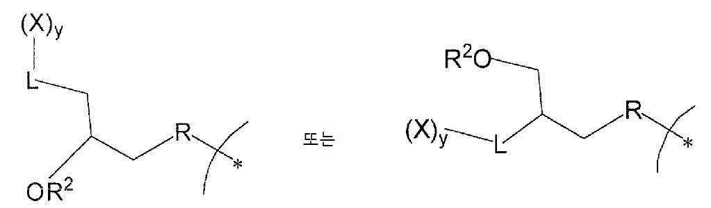
하나 이상의 실시형태에서, 비폴리머성 화합물은 둘 이상의 에폭시 잔기를 포함하며, 여기서 에폭시 잔기의 하나 이상은 하기의 화학식이다:In one or more embodiments, the nonpolymeric compound comprises two or more epoxy moieties, wherein one or more of the epoxy moieties is of the formula:

상기 화학식에서,In the above formula,
*은 화합물에 부착되는 부분이고, y는 각각 1-2이며, X는 각각 화학적 개질기이고, L은 각각 독립적으로 아미노, 에테르, 티오 (티오에테르), 히드라진, 설피네이트, 설포네이트, 설폰아미드, 에스테르, 카르보네이트, 카르바메이트, 아미드, 또는 우레아 결합이며, R는 각각 독립적으로 산소 원자 또는 -CH2이고, R2는 각각 독립적으로 -H, 알킬, 설포네이트, 에스테르, 카르보네이트, 카르바메이트, 또는 그의 기능화된 유도체이다. 하나 이상의 X 기(예를 들어, y가 2인 경우)의 경우, 각각의 X는 “X1” 및 “X2”로 각각 지정될 수 있으며, 여기서 X1 및 X2는 동일하거나 상이할 수 있으며, X1 및 X2에 대한 가능한 치환기는 본 명세서에서 “X”에 대해 개시한 것과 동일하다. 예를 들어, -L-X의 실시형태는 -NX1X2, -OX, -SX, -N-N(X1X2), -S(O)X, -S(O)2X, -OS(O)2X, --O(C=O)X, -O(C=O)OX, -N(C=O)OX, -N(C=O)X, -N(C=O)N(X1X2), -NX1S(O)2X2 등을 포함한다.
* Is a moiety attached to the compound, y is each 1-2, X is each a chemical modifier, L is each independently amino, ether, thio (thioether), hydrazine, sulfinate, sulfonate, sulfonamide, Ester, carbonate, carbamate, amide, or urea bond, each R is independently an oxygen atom or -CH 2 , each R 2 is independently -H, alkyl, sulfonate, ester, carbonate, Carbamate, or functionalized derivatives thereof. For one or more X groups (eg, when y is 2), each X may be designated as “X 1 ” and “X 2 ”, where X 1 and X 2 may be the same or different. And possible substituents for X 1 and X 2 are the same as those disclosed for “X” herein. For example, embodiments of -LX are -NX 1 X 2 , -OX, -SX, -NN (X 1 X 2 ), -S (O) X, -S (O) 2 X, -OS (O ) 2 X, --O (C = O) X, -O (C = O) OX, -N (C = O) OX, -N (C = O) X, -N (C = O) N ( X 1 X 2 ), -NX 1 S (O) 2 X 2 , and the like.
하나 이상의 실시형태에서, X는 각각 독립적으로 수소, 아릴기(Ar), (C1-C12)-직선형 또는 분지형(straight or branched) 알킬, (C1-C12) 직선형 또는 분지형 알켄일 또는 알킨일, (C1-C12) 시클로알킬 치환된 (C1-C12)-직선형 또는 분지형 알킬, (C1-C12) 시클로알킬 치환된-(C2-C6) 직선형 또는 분지형 알켄일 또는 알킨일, (C5-C7) 시클로알켄일 치환된-(C1-C12) 직선형 또는 분지형 알킬, (C5-C7) 시클로알켄일 치환된-(C1-C12) 직선형 또는 분지형 알켄일 또는 알킨일, 아릴-치환된 (C1-C12) 직선형 또는 분지형 알킬, 또는 아릴-치환된-(C1-C12) 직선형 또는 분지형 알켄일 또는 알킨일이며; X에서 알킨일, 알켄일 또는 알킬 사슬의 CH2 기의 하나는 (또는 그 이상은) O, CF2, S, S(O), S(O)2 또는 N(R5)에 의해 선택적으로 대체된다. R5는 H, S(O)2X, (C=O)X, (C=O)OX, (C=O)N(X)2, 아릴, (C1-C12)-직선형 또는 분지형 알킬, (C1-C12) 직선형 또는 분지형 알켄일 또는 알킨일, (C1-C12)시클로알킬 치환된 (C1-C12)-직선형 또는 분지형 알킬, (C1-C12)시클로알킬 치환된-(C2-C6) 직선형 또는 분지형 알켄일 또는 알킨일, (C5-C7) 시클로알켄일 치환된-(C1-C12) 직선형 또는 분지형 알킬, (C5-C7) 시클로알켄일 치환된-(C1-C12) 직선형 또는 분지형 알켄일 또는 알킨일, 아릴-치환된 (C1-C12) 직선형 또는 분지형 알킬, 또는 아릴-치환된-(C1-C12) 직선형 또는 분지형 알켄일 또는 알킨일에 의해 선택적으로 치환되며, 여기서 X에서 알킨일, 알켄일 또는 알킬 사슬의 CH2 기의 하나는 (또는 그 이상은) O, CF2, S, S(O), S(O)2 또는 N(R5)에 의해 선택적으로 대체된다. 일부 실시형태에서, y는 2인 경우, 두 개의 X 기는 함께 결합되어 피페리딘 고리의 경우에서처럼, L 기와 고리를 형성할 수 있다.
In one or more embodiments, each X is independently hydrogen, an aryl group (Ar), (C 1 -C 12 ) -straight or branched alkyl, (C 1 -C 12 ) straight or branched egg Kenyl or alkynyl, (C 1 -C 12 ) cycloalkyl substituted (C 1 -C 12 ) -linear or branched alkyl, (C 1 -C 12 ) cycloalkyl substituted- (C 2 -C 6 ) straight Or branched alkenyl or alkynyl, (C 5 -C 7 ) cycloalkenyl substituted- (C 1 -C 12 ) straight or branched alkyl, (C 5 -C 7 ) cycloalkenyl substituted- (C 1 -C 12 ) straight or branched alkenyl or alkynyl, aryl-substituted (C 1 -C 12 ) straight or branched alkyl, or aryl-substituted- (C 1 -C 12 ) straight or branched al Kenyl or alkynyl; One (or more) of CH 2 groups in the alkynyl, alkenyl or alkyl chain at X is optionally selected from O, CF 2 , S, S (O), S (O) 2 or N (R 5 ) Replaced. R 5 is H, S (O) 2 X, (C═O) X, (C═O) OX, (C═O) N (X) 2 , aryl, (C 1 -C 12 ) -linear or minute Topographic alkyl, (C 1 -C 12 ) straight or branched alkenyl or alkynyl, (C 1 -C 12 ) cycloalkyl substituted (C 1 -C 12 ) -linear or branched alkyl, (C 1 -C 12 ) cycloalkyl substituted- (C 2 -C 6 ) straight or branched alkenyl or alkynyl, (C 5 -C 7 ) cycloalkenyl substituted- (C 1 -C 12 ) straight or branched alkyl, (C 5 -C 7 ) cycloalkenyl substituted- (C 1 -C 12 ) straight or branched alkenyl or alkynyl, aryl-substituted (C 1 -C 12 ) straight or branched alkyl, or aryl- Optionally substituted by substituted- (C 1 -C 12 ) straight or branched alkenyl or alkynyl, wherein at X one of the CH 2 groups of the alkynyl, alkenyl or alkyl chain is (or more) Optionally substituted by O, CF 2 , S, S (O), S (O) 2 or N (R 5 ). In some embodiments, when y is 2, two X groups can be joined together to form a ring with an L group, as in the case of a piperidine ring.
X의 비제한적 예는 페닐, 1-나프틸, 2-나프틸, 인데닐, 아줄레닐(azulenyl), 플루오레닐, 안트라세닐, 2-퓨릴, 3-퓨릴, 2-티에닐, 3-티에닐, 2-피리딜, 3-피리딜, 4-피리딜, 피롤릴, 옥사졸릴, 티아졸릴, 이미다졸릴, 피라졸릴, 2-피라졸리닐, 피라졸리디닐, 이속사졸릴, 이소티아졸릴, 1,2,3-옥사디아졸릴, 1,2,3-트리아졸릴, 1,2,3-티아디아졸릴, 1,3,4-티아디아졸릴, 1,2,4-트리아졸릴, 1,2,4-옥사디아졸릴, 1,2,4-티아디아졸릴, 벤즈옥사졸릴, 피리다지닐, 피리미디닐, 피라지닐, 1,3,5-트리아지닐, 1,3,5-트리티아닐, 인돌리지닐, 인돌릴, 이소인돌릴, 3H 인돌릴, 인돌리닐, 벤조[b]퓨라닐, 벤조[b]티오페닐, 1H-인다졸릴, 벤즈이미다졸릴, 벤즈티아졸릴, 퓨리닐, 4H-퀴놀리지닐, 퀴놀리닐, 1,2,3,4-테트라히드로-이소퀴놀리닐, 이소퀴놀리닐, 1,2,3,4-테트라히드로-이소퀴놀리닐, 시놀리닐(cinnolinyl), 프탈라지닐, 퀴나졸리닐(quinazolinyl), 퀸옥살리닐(quinoxalinyl), 1,8-나프티리디닐, 페리디닐, 카르바졸릴, 아크리디닐, 페나지닐(phenazinyl), 페노티아지닐 또는 펜옥사지닐과 같은 기를 포함한다. X는 임의의 화학적으로 가능한 모노-, 비(bi)- 또는 트리 환형 고리 시스템일 수 있으며, 여기서 각각의 고리는 5 내지 7개의 고리 원자로 구성되며, 각각의 고리는 N, N(R5), O, S, S(O), 또는 S(O)2로부터 독립적으로 선택된 0 내지 3개의 헤테로원자를 포함한다고 인식될 것이다. 아릴 또는 환형 X 기는 또한 할로겐, 히드록시, 니트로, -SO3H, 트리플루오로메틸, 트리플루오로메톡시, (C1-C6)-직선형 또는 분지형 알킬, (C1-C6)-직선형 또는 분지형 알켄일, O-[(C1-C6)-직선형 또는 분지형 알킬], O-[(C1-C6)-직선형 또는 분지형 알켄일], O-벤질, O-페닐, 1,2-메틸렌디옥시, -N(R5-R5), 카르복실, N-((C1-C5)-직선형 또는 분지형 알킬 또는 (C1-C6)-직선형 또는 분지형 알켄일) 카르복스아미드, N,N-디-((C1-C6)-직선형 또는 분지형 알킬 또는 (C2-C5)-직선형 또는 분지형 알켄일) 카르복스아미드, N-(C2-C5)-직선형 또는 분지형 알킬 또는 (C2-C5)-직선형 또는 분지형 알켄일) 설폰아미드, N,N-디-(C2-C5)-직선형 또는 분지형 알킬 또는 (C2-C5)-직선형 또는 분지형 알켄일) 설폰아미드, 모르폴리닐, 피페리디닐, OR5, CH2--(CH2)10-R5, O--(CH2)10-R5, (CH2)10--O--R5, 또는 CH=CH--R5로부터 독립적으로 선택된 하나 내지 세 개의 치환기와 선택적으로 치환될 수 있으며, 여기서 R5는 상기에서 정의된 것과 같으며, X에서 알킨일, 알켄일 또는 알킬 사슬의 CH2 기의 임의의 하나는 (또는 그 이상은) O, CF2, S, S(O), S(O)2 또는 N(R5)에 의해 선택적으로 대체된다.
Non-limiting examples of X include phenyl, 1-naphthyl, 2-naphthyl, indenyl, azulenyl, fluorenyl, anthracenyl, 2-furyl, 3-furyl, 2-thienyl, 3- Thienyl, 2-pyridyl, 3-pyridyl, 4-pyridyl, pyrrolyl, oxazolyl, thiazolyl, imidazolyl, pyrazolyl, 2-pyrazolinyl, pyrazolidinyl, isoxazolyl, isothia Zolyl, 1,2,3-oxadiazolyl, 1,2,3-triazolyl, 1,2,3-thiadiazolyl, 1,3,4-thiadiazolyl, 1,2,4-triazolyl, 1,2,4-oxadiazolyl, 1,2,4-thiadiazolyl, benzoxazolyl, pyridazinyl, pyrimidinyl, pyrazinyl, 1,3,5-triazinyl, 1,3,5- Tritianyl, indolinyl, indolyl, isoindoleyl, 3H indolyl, indolinyl, benzo [b] furanyl, benzo [b] thiophenyl, 1H-indazolyl, benzimidazolyl, benzthiazolyl, Purinyl, 4H-quinolininyl, quinolinyl, 1,2,3,4-tetrahydro-isoquinolinyl, isoquinolinyl, 1,2,3,4-tetrahydro-isoquinolinyl, Cynolinyl (cin nolinyl), phthalazinyl, quinazolinyl, quinoxalinyl, 1,8-naphthyridinyl, ferridinyl, carbazolyl, acridinyl, phenazinyl, phenazinyl, phenothiazinyl or Groups such as phenoxazinyl. X can be any chemically possible mono-, bi-, or tricyclic ring system, wherein each ring consists of 5 to 7 ring atoms, each ring being N, N (R 5 ), It will be appreciated that it contains 0 to 3 heteroatoms independently selected from O, S, S (O), or S (O) 2 . An aryl or cyclic X group is also halogen, hydroxy, nitro, -SO 3 H, trifluoromethyl, trifluoromethoxy, (C 1 -C 6 ) -linear or branched alkyl, (C 1 -C 6 )- Straight or branched alkenyl, O-[(C 1 -C 6 ) -linear or branched alkyl], O-[(C 1 -C 6 ) -linear or branched alkenyl], O-benzyl, O- Phenyl, 1,2-methylenedioxy, -N (R 5 -R 5 ), carboxyl, N-((C 1 -C 5 ) -linear or branched alkyl or (C 1 -C 6 ) -linear or Branched alkenyl) carboxamides, N, N-di-((C 1 -C 6 ) -linear or branched alkyl or (C 2 -C 5 ) -linear or branched alkenyl) carboxamides, N -(C 2 -C 5 ) -linear or branched alkyl or (C 2 -C 5 ) -linear or branched alkenyl) sulfonamides, N, N-di- (C 2 -C 5 ) -linear or branched Topographic alkyl or (C 2 -C 5 ) -linear or branched alkenyl) sulfonamides, morpholinyl, piperidinyl, OR 5 , CH 2- (CH 2 ) 10 -R 5 , O-(CH 2 ) May be optionally substituted with one to three substituents independently selected from 10 -R 5 , (CH 2 ) 10 -O--R 5 , or CH = CH--R 5 , wherein R 5 is As defined and any one of (or more) CH 2 groups of the alkynyl, alkenyl or alkyl chain in X is O, CF 2 , S, S (O), S (O) 2 or N Optionally substituted by (R 5 ).
예를 들어, 일부 실시형태에서 상기 조성물이 반사 방지 코팅으로서 사용되는 경우, X는 벤젠 (페닐 기), 나프탈렌 (예를 들어, 1-나프틸, 2-나프틸), 안트라센 (안트라세닐), 알킬 (바람직하게는 약 C1-C12, 및 보다 바람직하게는 약 C1-C8), 및 그의 치환된 유도체로 이루어진 군에서 선택된 발색단이다.
For example, in some embodiments where the composition is used as an antireflective coating, X is benzene (phenyl group), naphthalene (eg 1-naphthyl, 2-naphthyl), anthracene (anthracenyl), Chromophore selected from the group consisting of alkyl (preferably about C 1 -C 12 , and more preferably about C 1 -C 8 ), and substituted derivatives thereof.
상기에서 개시하였듯이, 에폭시 고리-열림 후에 전형적으로 존재하는 알코올 기는 필요에 따라, 알킬, 설폰네이트, 에스테르, 카르보네이트, 또는 카르바메이트 기를 사용하여 추가로 기능화될 수 있다. 예를 들어, 상기 R2 치환기의 기능화된 유도체는 S(O)2X, (C=O)X, (C=O)OX, (C=O)N(X1X2), 아릴, (C1-C12)-직선형 또는 분지형 알킬, (C1-C12)-직선형 또는 분지형 알켄일 또는 알킨일, (C1-C12) 시클로알킬 치환된 (C1-C12)-직선형 또는 분지형 알킬, (C1-C12) 시클로알킬 치환된-(C2-C6) 직선형 또는 분지형 알켄일 또는 알킨일, (C5-C7) 시클로알켄일 치환된-(C1-C10) 직선형 또는 분지형 알킬, (C5-C7) 시클로알켄일 치환된-(C1-C12) 직선형 또는 분지형 알켄일 또는 알킨일, 아릴-치환된-(C1-C12) 직선형 또는 분지형 알킬, 또는 아릴-치환된-(C1-C12) 직선형 또는 분지형 알켄일 또는 알킨일을 포함하며; 여기서 X는 상기에서 정의된 것과 같으며, R2에서 알킨일, 알켄일 또는 알킬 사슬의 임의의 하나의 CH2 기는 O, CF2, S, S(O), S(O)2 또는 N(R5)에 의해 선택적으로 대체되며, 상기 R5는 상기에서 정의된 것과 같다. 따라서, 상기에서 개시하였듯이, 비폴리머성 화합물은 연결 -L-를 통하여 부착된 X 기와 함께, 추가적인 X 기와 더 기능화될 수 있다.
As disclosed above, alcohol groups typically present after epoxy ring-opening can be further functionalized using alkyl, sulfonate, ester, carbonate, or carbamate groups, as desired. For example, the functionalized derivatives of the R 2 substituents include S (O) 2 X, (C═O) X, (C═O) OX, (C═O) N (X 1 X 2 ), aryl, ( C 1 -C 12 ) -linear or branched alkyl, (C 1 -C 12 ) -linear or branched alkenyl or alkynyl, (C 1 -C 12 ) cycloalkyl substituted (C 1 -C 12 )- Straight or branched alkyl, (C 1 -C 12 ) cycloalkyl substituted- (C 2 -C 6) straight or branched alkenyl or alkynyl, (C 5 -C 7 ) cycloalkenyl substituted- (C 1- C 10 ) straight or branched alkyl, (C 5 -C 7 ) cycloalkenyl substituted- (C 1 -C 12 ) straight or branched alkenyl or alkynyl, aryl-substituted- (C 1 -C 12 ) Straight or branched alkyl, or aryl-substituted- (C 1 -C 12 ) straight or branched alkenyl or alkynyl; Wherein X are the same as defined above, in R 2 alkynyl, alkenyl or alkyl chain, any one of the CH 2 groups O, CF 2, S, S (O), S (O) 2 or N ( Optionally substituted by R 5 ), wherein R 5 is as defined above. Thus, as disclosed above, the nonpolymeric compound can be further functionalized with additional X groups, with the X groups attached through the linking -L-.
하나 이상의 실시형태에서, 비폴리머성 화합물은 에폭시 및 아다만틸 잔기가 각각 결합되 있는 코어 구성요소를 더 포함한다. 다시 말해, 상기 에폭시 잔기는 바람직하게는 아다만틸 케이지 고리에 직접 연결되지 않는다. 상기 코어 구성요소의 구조는 에폭시 및 아다만틸 잔기와 결합할 수 있는 한, 중요하지 않다. 예시적인 코어 구성요소는 방향족 또는 지방족 환형 화합물, 비환형 화합물, 및 상기 화합물의 기능성 유도체로 이루어진 군으로부터 선택된 구조를 포함한다. 적절한 코어 구성요소의 구체 예는 시클로알칸, 헤테로시클, 방향족 고리 (예를 들어, 벤젠), 분지형 또는 선형(linear) 알킬, 알켄, 알카인 등의 기능성 유도체를 포함한다. 용어 “기능성 유도체(functional derivatives)”는 다른 화합물과 결합할 수 있도록, 구조가 변경된 화합물의 유도체를 의미한다. 예를 들어, 벤젠의 기능성 유도체는 벤젠 고리의 탄소 원자가 다른 화합물 또는 잔기와 결합할 수 있도록, 하나 이상의 수소 원자가 제거된 벤젠 고리를 포함한다. 일부 실시형태에서, 비폴리머성 화합물은 코어 구성요소, 둘 이상의 에폭시 잔기, 하나 이상의 아다만틸 기, 및 하나의 에폭시에 결합된 하나 이상의 화학적 개질기로 필수적으로 구성되거나 또는 이들로 구성되기도 한다.
In one or more embodiments, the nonpolymeric compound further comprises a core component to which the epoxy and adamantyl residues are each bonded. In other words, the epoxy moiety is preferably not directly linked to the adamantyl cage ring. The structure of the core component is not critical as long as it can bond with epoxy and adamantyl moieties. Exemplary core components include structures selected from the group consisting of aromatic or aliphatic cyclic compounds, acyclic compounds, and functional derivatives of these compounds. Specific examples of suitable core components include functional derivatives such as cycloalkanes, heterocycles, aromatic rings (eg benzene), branched or linear alkyls, alkenes, alkines and the like. The term “functional derivatives” refers to derivatives of compounds whose structure has been altered so that they can bind with other compounds. For example, functional derivatives of benzene include benzene rings from which one or more hydrogen atoms have been removed, such that the carbon atoms of the benzene ring can bond with other compounds or residues. In some embodiments, the nonpolymeric compound consists essentially of or consists of a core component, two or more epoxy moieties, one or more adamantyl groups, and one or more chemical modifiers bonded to one epoxy.
하나 이상의 실시형태에서, 본 발명에 따른 비폴리머성 화합물은 하기의 일반적인 화학식을 포함할 것이다(필수적으로 구성되거나 구성되기도 할 것이다):In one or more embodiments, the nonpolymeric compound according to the invention will comprise (and may consist essentially of) the following general formula:

상기 식에서,Where
m은 2 이상 (바람직하게는 2-4)이며, n은 1 이상 (바람직하게는 1-2)이며, Y는 상기에서 정의된 것과 같은 코어 구성요소이며; R은 각각 독립적으로 산소 원자 또는 -CH2-이며, R3 및 R4는 특정 화합물에서 서로 상이하며 각각 -L-(X)y 및 -OR2로 이루어진 군으로부터 선택되며, 여기에서 L은 각각 독립적으로 아미노, 에테르, 티오 (티오에테르), 히드라진, 설피네이트, 설포네이트, 설폰아미드, 에스테르, 카르보네이트, 카르바메이트, 아미드, 또는 우레아 연결기이며, y는 1-2이며, X는 화학적 개질기이며, R2는 각각 독립적으로 -H, 알킬, 설포네이트, 에스테르, 카르보네이트, 카르바네이트, 또는 그의 기능화된 유도체이다.
m is at least 2 (preferably 2-4), n is at least 1 (preferably 1-2) and Y is a core component as defined above; R are each independently an oxygen atom or -CH 2- , R 3 and R 4 are different from each other in a particular compound and are each selected from the group consisting of -L- (X) y and -OR 2 , where L is each Independently amino, ether, thio (thioether), hydrazine, sulfinate, sulfonate, sulfonamide, ester, carbonate, carbamate, amide, or urea linking group, y is 1-2, X is chemical reformer, and, R 2 are each independently -H, alkyl, sulfonate, ester, carbonate, carbamate carbonate, or a functionalized derivative thereof.
실시형태와 상관없이, 이들 화합물은 반사 방지 코팅 또는 평탄화 층과 같이, 마이크로리소그래피 공정에서 사용되는 조성물을 만드는데 사용될 수 있다. 상기 화합물은 적절한 용매 계에서, 바람직하게는 실질적으로 균일한 분산액을 형성하기 위해 주변 조건에서 충분한 시간 동안 비폴리머성 화합물을 간단히 분산 또는 용해함으로써 형성된다. 바람직한 조성물은 조성물 중에서 고형물의 총 무게 100 중량%를 기준으로, 비폴리머성 화합물의 약 0.5 내지 약 50 중량%, 바람직하게는 비폴리머성 화합물의 약 1 내지 약 20 중량%, 보다 바람직하게는 비폴리머성 화합물의 약 1 내지 약 5 중량%를 포함한다. 하나 이상의 실시형태에서, 본 발명에 따른 조성물은 바람직하게는 실질적으로 비폴리머성이다(즉, 조성물 중에서 고형물의 총 무게 100 중량%를 기준으로, 폴리머성 성분의 약 10 중량% 미만, 보다 바람직하게는 폴리머성 성분의 약 5 중량% 미만, 보다 더 바람직하게는 폴리머성 성분의 약 1 중량% 미만을 포함한다).
Regardless of the embodiment, these compounds can be used to make compositions used in microlithography processes, such as antireflective coatings or planarization layers. The compound is formed by simply dispersing or dissolving the nonpolymeric compound in a suitable solvent system, preferably for sufficient time at ambient conditions to form a substantially uniform dispersion. Preferred compositions comprise from about 0.5 to about 50 weight percent of the nonpolymeric compounds, preferably from about 1 to about 20 weight percent of the nonpolymeric compounds, more preferably based on 100 weight percent of the total weight of solids in the composition. About 1 to about 5 weight percent of the polymeric compound. In at least one embodiment, the composition according to the invention is preferably substantially nonpolymeric (ie less than about 10% by weight of the polymeric component, more preferably based on 100% by weight total weight of solids in the composition). Comprises less than about 5% by weight of the polymeric component, even more preferably less than about 1% by weight of the polymeric component).
용매 계는 마이크로 전자 제조용으로 적합한 임의의 용매를 포함할 수 있다. 바람직하게는, 용매 계는 약 100℃ 내지 약 200℃의 끓는점을 갖는다. 하나 이상의 실시형태에서, 용매 계는 프로필렌 글리콜 모노메틸 에테르(PGME), 프로필렌 글리콜 모노메틸 에테르 아세테이트(PGMEA), 에틸 락테이트, 프로필렌 글리콜 n-프로필 에테르(PnP), 시클로헥산온, 테트라히드로퓨란(THF), 디메틸 포름아미드(DMF), γ-부티로락톤(butyrolactone), 및 그의 혼합물로 이루어진 군에서 선택된 용매를 포함할 것이다.
The solvent system can include any solvent suitable for microelectronics manufacturing. Preferably, the solvent system has a boiling point of about 100 ° C to about 200 ° C. In one or more embodiments, the solvent system is propylene glycol monomethyl ether (PGME), propylene glycol monomethyl ether acetate (PGMEA), ethyl lactate, propylene glycol n-propyl ether (PnP), cyclohexanone, tetrahydrofuran ( THF), dimethyl formamide (DMF), γ-butyrolactone, and mixtures thereof.
임의의 추가적인 성분은 비폴리머성 화합물과 함께 용매 계에서 분산될 수 있다. 적절한 추가적인 성분의 예는 가교제, 촉매, 폴리머성 첨가제, 및 계면활성제를 포함한다. 일부 실시형태에서, 조성물은 실질적으로 폴리머성 첨가제를 함유하지 않는다. 다시 말해, 상기 성분은 고형물의 총 무게 100 중량%를 기준으로, 약 0.01 중량% 미만, 바람직하게는 약 0.001 중량% 미만의 정도로 존재한다. 하나 이상의 실시형태에서, 반사 방지 또는 평탄화 조성물은 상기 조성물에 포함되는 것으로 본 명세서에서 설명한 상기 추가적인 성분과 함께 용매 계에서 분산되거나 용해된 비폴리머성 화합물로 필수적으로 구성되거나 또는 이들로 구성되기도 한다. 다시 말해, 일부 실시형태에서, 본 발명의 조성물은 본 명세서에서 구체적으로 열거되지 않은 임의의 다른 성분들을 배제한다.
Any additional component may be dispersed in the solvent system with the nonpolymeric compound. Examples of suitable additional components include crosslinkers, catalysts, polymeric additives, and surfactants. In some embodiments, the composition is substantially free of polymeric additives. In other words, the component is present in an amount of less than about 0.01 wt%, preferably less than about 0.001 wt%, based on 100 wt% of the total weight of solids. In one or more embodiments, the antireflective or planarizing composition is comprised essentially of or consists of a nonpolymeric compound dispersed or dissolved in a solvent system with the additional components described herein as included in the composition. In other words, in some embodiments, the composition of the present invention excludes any other component not specifically listed herein.
예를 들어, 일부 실시형태에서, 본 조성물은 가교제와 함께 용매 계에서 분산되거나 용해된 비폴리머성 화합물로 필수적으로 구성되거나 또는 이들로 구성되기도 한다. 가교제가 존재하는 경우, 상기 조성물은 조성물 중에서 고형물의 총 무게 100 중량%를 기준으로, 약 40 중량% 미만의 가교제, 바람직하게는 약 0.05 내지 약 40 중량%의 가교제, 보다 바람직하게는 약 5 내지 약 30 중량%의 가교제를 포함할 수 있다. 본 발명의 일부 실시형태에서 사용될 수 있는 예시적인 가교제는 아미노플라스트(aminoplast)(예를 들어, POWDERLINK® 1174, Cymel® 제품), 다기능성 에폭시 수지(예를 들어, MY720, CY179MA, DENACOL), 안하이드라이드, 비닐 에테르(예를 들어, VECTomerTM과 같은 다기능성 비닐 에테르) 및 그의 혼합물을 포함한다.
For example, in some embodiments, the present compositions consist essentially of or consist of nonpolymeric compounds dispersed or dissolved in a solvent system with a crosslinking agent. If present, the composition comprises less than about 40% by weight of crosslinking agent, preferably from about 0.05 to about 40% by weight of crosslinking agent, more preferably from about 5% by weight, based on 100% by weight of total weight of solids in the composition. About 30% by weight crosslinker. Exemplary crosslinking agents which can be used in some embodiments of the present invention, aminoplast (aminoplast) (e.g., POWDERLINK ® 1174, Cymel ® products), multifunctional epoxy resins (e.g., MY720, CY179MA, DENACOL), Anhydrides, vinyl ethers (eg, multifunctional vinyl ethers such as VECTomer ™ ) and mixtures thereof.
바람직한 촉매의 예는 설폰산(예를 들어, p-톨루엔설폰산, 스티렌 설폰산), 광산 발생제(photoacid generator)(예를 들어, 트리페닐 설포늄 트리플레이트, 트리페닐 설포늄 노나플레이트(nonaflate)), 열산 발생제(thermal acid generator) (예를 들어, 피리디늄 토실레이트), 카르복실산(예를 들어, 트리클로로아세트산, 벤젠 테트라카르복실산), 인산 및 그의 혼합물을 포함한다. 촉매가 존재하는 경우, 상기 조성물은 조성물 중에서의 고형물의 총 무게 100 중량%를 기준으로, 약 10 중량% 미만의 촉매, 바람직하게는 약 0.01 내지 약 10 중량%의 촉매, 및 보다 바람직하게는 약 0.01 내지 약 5 중량%의 촉매를 포함할 수 있다.
Examples of preferred catalysts include sulfonic acid (eg p-toluenesulfonic acid, styrene sulfonic acid), photoacid generators (eg triphenyl sulfonium triflate, triphenyl sulfonium nonalate ), Thermal acid generators (eg pyridinium tosylate), carboxylic acids (eg trichloroacetic acid, benzene tetracarboxylic acid), phosphoric acid and mixtures thereof. If present, the composition comprises less than about 10 weight percent of the catalyst, preferably from about 0.01 to about 10 weight percent of the catalyst, and more preferably, about 100 weight percent of the total weight of solids in the composition. 0.01 to about 5% by weight of catalyst may be included.
하나 이상의 실시형태에서, 계면활성제는 조성물의 코팅 품질을 향상시키기 위해서 조성물 중에 포함될 수 있다. 사용될 수 있는 예시적인 계면활성제는 퍼플루오로 알킬 등을 포함한다. 계면활성제가 존재하는 경우, 상기 조성물은 조성물 중에서의 고형물의 총 무게 100 중량%를 기준으로,약 1 중량% 미만의 계면활성제, 바람직하게는 약 0.001 내지 약 1 중량%의 계면활성제, 및 보다 바람직하게는 약 0.001 내지 약 0.05 중량%의 계면활성제를 포함할 수 있다.
In one or more embodiments, surfactants may be included in the composition to improve the coating quality of the composition. Exemplary surfactants that can be used include perfluoro alkyl and the like. If present, the composition is less than about 1% by weight of surfactant, preferably from about 0.001 to about 1% by weight, and more preferably, based on 100% by weight total weight of solids in the composition Preferably from about 0.001 to about 0.05% by weight of the surfactant.
상기에서 언급하였듯이, 본 조성물은 마이크로 전자 제조에서 반사 방지 또는 평탄화 코팅에 있어서 특히 유용하다. 예를 들어, 코팅은 기판 표면 위에 조성물의 층을 형성하기 위해서, 기판에 본 발명의 조성물을 다량 도포함으로써 기판 위에 형성될 수 있다. 상기 조성물은 기판 표면 위에 형성되는 하나 이상의 선택적인 중간 하지층의 가장 위층이나, 기판 표면에 직접적으로 도포될 수 있다. 적절한 중간 하지층은 스핀-온(spin-on) 탄소층(SOC), 비정질 탄소층, 평탄화 층, 바닥 반사 방지 코팅, 및 그의 조합으로 이루어진 군으로부터 선택된 것을 포함한다. 그러나, 일부 실시형태에서, 반사 방지 또는 평탄화 조성물은 임의의 탄소가 풍부한 층 대신에 마이크로 전자 구조에서 존재할 수 있다. 다시 말해, 마이크로 전자 구조는 스택(stack)에서 다른 탄소가 풍부한 층을 갖지 않을 수 있다. 본 명세서에서 사용되는 용어 “탄소가 풍부한(carbon-rich)”은 조성물 중에 고형물의 총 무게 100 중량%를 기준으로 약 50 중량% 초과의 탄소, 바람직하게는 약 70 중량% 초과의 탄소, 보다 바람직하게는 약 75 내지 약 80 중량%의 탄소를 포함하는 조성물을 의미한다.
As mentioned above, the compositions are particularly useful for antireflective or planarizing coatings in microelectronics manufacturing. For example, a coating can be formed on a substrate by applying a large amount of the composition of the present invention to the substrate to form a layer of the composition on the substrate surface. The composition may be applied directly to the substrate surface or to the top layer of one or more optional intermediate underlying layers formed on the substrate surface. Suitable intermediate base layers include those selected from the group consisting of spin-on carbon layers (SOC), amorphous carbon layers, planarization layers, bottom antireflective coatings, and combinations thereof. However, in some embodiments, the antireflective or planarizing composition may be present in the microelectronic structure instead of any carbon rich layer. In other words, the microelectronic structure may not have other carbon rich layers in the stack. As used herein, the term “carbon-rich” means more than about 50 weight percent carbon, preferably more than about 70 weight percent carbon, more preferably based on 100 weight percent total weight of solids in the composition. Preferably a composition comprising from about 75 to about 80 weight percent carbon.
임의의 마이크로 전자 기판이 본 발명에 사용될 수 있다. 바람직한 기판은 실리콘, SiGe, SiO2, Si3N4, 알루미늄, 텅스텐, 텅스텐 실리사이드, 갈륨 비소(gallium arsenide), 게르마늄, 탄탈륨, 질화 탄탈륨, 산호, 블랙 다이아몬드, 인 또는 붕소가 도핑된 유리, 이온 주입층, 질화 티타늄, 하프늄 산화물(hafnium oxide), 실리콘 산화질소, 및 그의 혼합물로 이루어진 군에서 선택된 것을 포함한다. 상기 조성물은 약 750rpm 내지 약 5,000rpm (바람직하게는 약 750rpm 내지 약 4,000rpm, 보다 바람직하게는 약 1,000rpm 내지 약 3,500rpm)의 속도로, 약 20초 내지 약 90초 (바람직하게는 약 30초 내지 약 60초)의 시간 동안, 조성물을 스핀-코팅하는 하나의 바람직한 방법을 포함하여, 임의의 공지된 적용 방법에 의해 도포될 수 있다. 기판은 평면 표면을 가질 수 있거나, (홀, 트랜치(trench), 콘택트 홀, 양각부(raised feature), 선 등을 통하여) 토포그래피 피처(feature)를 포함할 수 있다. 본 명세서에서 사용되는, 용어 “토포그래피(topography)”는 기판 표면 위 또는 안에서의 구조의 깊이 또는 높이를 의미한다. 예를 들어, 기판은 측벽과 하부벽을 포함하여, 홀을 정의하는 구조를 포함할 수 있다. 따라서, 기판에 반사 방지 또는 평탄화 조성물을 도포하는 방법은 바람직하게는 상기 홀의 측벽과 하부벽의 적어도 일부분에 조성물을 도포하는 것을 포함할 수 있다.
Any microelectronic substrate can be used in the present invention. Preferred substrates are silicon, SiGe, SiO 2 , Si 3 N 4 , aluminum, tungsten, tungsten silicide, gallium arsenide, germanium, tantalum, tantalum nitride, coral, black diamond, phosphorus or boron doped glass, ions Injection layer, titanium nitride, hafnium oxide, silicon oxide nitrogen, and mixtures thereof. The composition is about 20 seconds to about 90 seconds (preferably about 30 seconds) at a speed of about 750 rpm to about 5,000 rpm (preferably about 750 rpm to about 4,000 rpm, more preferably about 1,000 rpm to about 3,500 rpm). To about 60 seconds), can be applied by any known method of application, including one preferred method of spin-coating the composition. The substrate may have a planar surface or may include topographic features (via holes, trenches, contact holes, raised features, lines, etc.). As used herein, the term “topography” refers to the depth or height of a structure on or within a substrate surface. For example, the substrate can include a structure defining a hole, including sidewalls and bottom walls. Thus, the method of applying the antireflective or planarizing composition to the substrate may preferably comprise applying the composition to at least a portion of the sidewalls and bottom walls of the holes.
바람직한 커버(coverage)가 이루어진 후에, 조성물의 층을 가열하여서 용매를 증발시키고 경화층을 형성하였다. 바람직하게는 상기 층은 약 125℃ 이상의 온도, 바람직하게는 약 150℃ 내지 약 230℃의 온도, 보다 바람직하게는 약 150℃ 내지 약 205℃의 온도로, 약 30초 내지 약 90초 (바람직하게는 약 45초 내지 약 75초)의 시간 동안 가열된다. 하나 이상의 실시형태에서, 본 발명의 층을 경화(curing)하는 것은 조성물에서 비폴리머성 화합물을 가교하는 것을 포함한다. 따라서, 일부 실시형태에서, 층은 조성물의 대략 가교 온도 이상 (예를 들어, 약 150℃ 이상)으로 가열된다. 비폴리머성 화합물의 가교는 조성물의 화학적 개질기에서 자유 반응성 잔기 (예를 들어, -OH 기)를 통하여 발생할 수 있다. 유사하게, 가교는 고리-열림 에폭시 잔기에서 자유 -OH 기를 통하여 또는 화학적 개질 잔기에서 다른 적절한 기능성 기를 통하여 개시될 수 있다. 따라서, 적절한 가교 부분은 (필요한 경우) 선택된 가교제의 유형에 따라서 다양해질 수 있다. 일부 실시형태에서, 비폴리머성 화합물은 화학적 개질기의 반응성 잔기에 따라서 가교제의 도움 없이 자기-가교(self-crosslink)할 수 있다. 상기에서 언급하였듯이, 아다만틸 기는 바람직하게는 가교에 참여하지 않는다. After the desired coverage was achieved, the layers of the composition were heated to evaporate the solvent and form a cured layer. Preferably the layer is at a temperature of at least about 125 ° C., preferably at a temperature of about 150 ° C. to about 230 ° C., more preferably at a temperature of about 150 ° C. to about 205 ° C., from about 30 seconds to about 90 seconds (preferably Is heated for a time from about 45 seconds to about 75 seconds). In one or more embodiments, curing the layer of the present invention comprises crosslinking the nonpolymeric compound in the composition. Thus, in some embodiments, the layer is heated above about the crosslinking temperature of the composition (eg, above about 150 ° C.). Crosslinking of nonpolymeric compounds may occur via free reactive moieties (eg, —OH groups) in the chemical modifiers of the composition. Similarly, crosslinking can be initiated via free —OH groups at ring-open epoxy residues or through other suitable functional groups at chemically modified residues. Thus, suitable crosslinking moieties may vary depending on the type of crosslinking agent selected (if necessary). In some embodiments, the nonpolymeric compound may self-crosslink without the aid of a crosslinker, depending on the reactive moiety of the chemical modifier. As mentioned above, the adamantyl group preferably does not participate in crosslinking.
실시형태와 상관없이, 본 발명의 경화된 코팅 또는 필름의 평균 두께는 바람직하게는 약 5nm 내지 약 5μm, 보다 바람직하게는 약 10nm 내지 약 3μm, 보다 더 바람직하게는 약 20nm 내지 약 2μm이다. 기판이 토포그래피를 포함하는 경우, 본 발명의 코팅은 바람직하게는 상기 두께에서 기판 토포그래피를 실질적으로 덮기에 충분한 두께를 갖는다. 평균 두께는 엘립소미터를 사용하여 기판을 통해 5회 측정하여 평균한 것으로 정의된다.
Regardless of the embodiment, the average thickness of the cured coatings or films of the present invention is preferably from about 5 nm to about 5 μm, more preferably from about 10 nm to about 3 μm, even more preferably from about 20 nm to about 2 μm. If the substrate comprises topography, the coating of the present invention preferably has a thickness sufficient to substantially cover the substrate topography at that thickness. The average thickness is defined as the average of five measurements through the substrate using an ellipsometer.
본 발명에 따른 경화층은 포토레지스트에 전형적으로 사용되는 용매 (예를 들어, 에틸 락테이트, PGME) 중에, 실질적으로 불용성일 수 있다. 따라서, 박리(stripping) 시험의 경우, 본 발명의 코팅은 약 5% 미만, 바람직하게는 약 1% 미만, 보다 바람직하게는 약 0%의 퍼센트(%) 박리를 가질 수 있다. 박리 시험은 (5개의 상이한 위치에서 측정한 것의 평균을 계산함으로써) 경화층의 두께를 먼저 결정하는 것을 포함한다. 이것은 평균 초기 필름 두께이다. 다음에, 용매를 약 20초 동안 경화된 필름 위에 퍼들(puddle)한 다음, 약 3,000rpm에서 약 30초 동안 스핀 건조하여서 용매를 제거하였다. 두께를 엘립소미터를 사용하여 웨이퍼(wafer) 위의 다섯 개의 상이한 지점에서 다시 측정하고, 상기 측정 값의 평균을 결정한다. 이것이 평균 최종 필름 두께이다. 박리의 양은 초기와 최종 평균 필름 두께 간의 차이에 해당한다. 상기 박리 퍼센트는 다음과 같다:The cured layer according to the present invention may be substantially insoluble in solvents typically used in photoresists (eg, ethyl lactate, PGME). Thus, for the stripping test, the coating of the present invention may have a percent (%) peel of less than about 5%, preferably less than about 1%, more preferably about 0%. The peel test involves first determining the thickness of the cured layer (by calculating the average of what was measured at five different locations). This is the average initial film thickness. The solvent was then puddle on the cured film for about 20 seconds and then spin dried at about 3,000 rpm for about 30 seconds to remove the solvent. The thickness is measured again at five different points on the wafer using an ellipsometer and the average of the measured values is determined. This is the average final film thickness. The amount of exfoliation corresponds to the difference between the initial and final average film thickness. The percent peel is as follows:

본 발명의 경화층은 또한 바람직하게는 전형적인 포토레지스트 현상액(developer) (예를 들어, 테트라메틸암모늄 히드록사이드(TMAH)) 중에 실질적으로 불용성이다. 현상액에서 본 발명의 필름의 용해도는 포토레지스트 용매 대신에 현상액이 사용되는 것을 제외하고는, 상기에서 설명한 박리 시험에서와 동일한 과정 및 계산법을 사용하여 측정하였다. 또한, 가교된 층을 110℃에서 60초 동안 PEB를 한다. 다음에, 0.26N TMAH 현상액을 45초 동안 층 위에 첨가하며, 이어서 5초 동안 탈이온수로 헹구고, 스핀 건조시킨다. 경화층에서 임의의 두께 손실은 “다크 로스(dark loss)”로 정의된다. 경화층은 약 5% 미만의 다크 로스, 바람직하게는 약 1.5% 미만의 다크 로스, 보다 바람직하게는 약 1% 미만의 다크 로스, 보다 더 바람직하게는 약 0.8% 미만의 다크 로스, 가장 바람직하게는 약 0%의 다크 로스를 가질 수 있다.
The cured layer of the present invention is also preferably substantially insoluble in typical photoresist developers (eg, tetramethylammonium hydroxide (TMAH)). The solubility of the film of the present invention in the developer was measured using the same procedure and calculation method as in the peel test described above, except that a developer was used instead of a photoresist solvent. In addition, the crosslinked layer was PEB for 60 seconds at 110 ℃. Next, 0.26N TMAH developer is added over the layer for 45 seconds, then rinsed with deionized water for 5 seconds and spin dried. Any thickness loss in the hardened layer is defined as "dark loss". The cured layer has less than about 5% dark loss, preferably less than about 1.5% dark loss, more preferably less than about 1% dark loss, even more preferably less than about 0.8% dark loss, most preferably May have a dark loss of about 0%.
본 발명에 따른 코팅은 높은 에칭 비율을 가진다. 따라서, 경화된 코팅은 CF4가 에칭액(etchant)로서 사용되는 경우, 약 2 Å/초 이상의 에칭 비율, 바람직하게는 약 2 내지 약 10 Å/초의 에칭 비율, 보다 바람직하게는 약 3 Å/초 내지 약 7 Å/초의 에칭 비율, 보다 더 바람직하게는 약 4 Å/초 내지 약 6 Å/초의 에칭 비율을 갖는다. O2가 에칭액으로 사용되는 경우, 경화형 코팅은 약 10 Å/초 이상의 에칭 비율, 바람직하게는 약 10 내지 약 50 Å/초의 에칭 비율, 보다 바람직하게는 약 15 Å/초 내지 약 40 Å/초의 에칭 비율, 보다 더 바람직하게는 약 20 Å/초 내지 약 35 Å/초의 에칭 비율을 갖는다. 반사 방지 코팅으로서 사용되는 경우, 상기 층은 바람직하게는 광 흡수 특성을 갖는다. 예를 들어, 193nm 또는 248nm에서 경화형 반사 방지층의 굴절률(n 값)은 약 1.2 이상, 바람직하게는 약 1.3 내지 약 2, 보다 바람직하게는 약 1.4 내지 약 1.8일 수 있다. 반사 방지층은 사용 파장(예를 들어, 193nm, 248nm, 또는 365nm)에서, 약 0.001 이상, 바람직하게는 약 0.01 내지 약 0.8, 보다 바람직하게는 약 0.05 내지 약 0.6의 흡광 계수(extinction coefficient, k 값)을 갖는다. 코팅은 193nm 포토레지스트에서 약 100μm 미만의 해상도(resolution), 바람직하게는 약 50μm 미만의 해상도를 얻기 위해 사용될 수 있다.
The coating according to the invention has a high etching rate. Thus, the cured coating has an etching rate of at least about 2 kPa / sec, preferably about 2 to about 10 kPa / sec, more preferably about 3 kPa / sec, when CF 4 is used as an etchant. To an etching rate of from about 7 kPa / sec, even more preferably from about 4 kPa / sec to about 6 kPa / sec. When O 2 is used as the etchant, the curable coating has an etching rate of at least about 10 kPa / sec, preferably from about 10 to about 50 kPa / sec, more preferably from about 15 kPa / sec to about 40 kPa / sec. An etch rate, even more preferably from about 20 kPa / sec to about 35 kPa / sec. When used as an antireflective coating, the layer preferably has light absorbing properties. For example, the refractive index (n value) of the curable antireflective layer at 193 nm or 248 nm may be about 1.2 or more, preferably about 1.3 to about 2, more preferably about 1.4 to about 1.8. The antireflective layer has an extinction coefficient, k value of at least about 0.001, preferably from about 0.01 to about 0.8, more preferably from about 0.05 to about 0.6, at the wavelength of use (eg, 193 nm, 248 nm, or 365 nm). Has The coating can be used to obtain a resolution of less than about 100 μm, preferably less than about 50 μm, in a 193 nm photoresist.
다음, 감광성(photosensitive) 조성물을 본 발명의 층에 도포하고, 이어서 도포 후 베이킹(post application bake, PAB)을 하여서, 이미지층(imaging layer)을 형성할 수 있다. 이미지층의 두께는 전형적으로 약 50nm 내지 약 2,000nm의 범위일 수 있다. 적절한 이미지화 조성물은 상업적으로 입수가능한 포토레지스트 (예를 들어, (일본) 가나가와현, 가와사키 시, TOK의 TarF-Pi6-001; 미국 캘리포니아, 서니베일, JSR Micro의 ARX3001JN, ARX3340J, 및 AM2073J; (일본) 도쿄, 신에츠(Shin-Etsu)의 SAIL-X-181), 또는 임의의 다른 감광성 조성물을 포함한다. 이미지층은 적절한 파장의 빛으로의 노광, 이어서 노광 후 베이킹(post-exposure bake(PEB)), 및 패턴의 성장(development)에 의해 패턴화될 수 있다. 적절한 현상액은 수산화칼륨(KOH), TMAH와 같은 유기 또는 무기 알칼리 용액이며, 바람직하게는 0.26N 이하의 농도에서 TMAH의 수용액을 포함한다. 상기 현상액의 일부는 상품명 PD523AD (미국 워싱턴, 모세 레이크, 모세 레이크 사(Moses Lake Industies, Inc.)로부터 입수가능함), MF-319(다우 케미칼(Dow Chemical) 사로부터 입수가능함), MF-320(시플리(Shipley) 사로부터 입수가능함), 및 NMD3(일본, TOK 사로부터 입수가능함)로부터 상업적으로 입수가능하다.
Next, a photosensitive composition can be applied to the layer of the invention, followed by a post application bake (PAB) to form an imaging layer. The thickness of the image layer may typically range from about 50 nm to about 2,000 nm. Suitable imaging compositions include commercially available photoresists (e.g., TarF-Pi6-001, Kanagawa Prefecture, Kawasaki City, TOK; California, Sunnyvale, USA; ARX3001JN, ARX3340J, and AM2073J; (Japan) ) SAIL-X-181 from Tokyo, Shin-Etsu), or any other photosensitive composition. The image layer may be patterned by exposure to light of an appropriate wavelength, followed by post-exposure bake (PEB), and development of the pattern. Suitable developer is an organic or inorganic alkaline solution such as potassium hydroxide (KOH), TMAH, and preferably comprises an aqueous solution of TMAH at a concentration of 0.26 N or less. Some of these developer solutions are available under the trade names PD523AD (available from Moses Lake Industies, Inc., Washington, USA), MF-319 (available from Dow Chemical), MF-320 (available from Dow Chemical). Commercially available from Shipley, and NMD3 (available from TOK, Japan).
다른 실시형태에서, ArF 담금(immersion) 리소그래피는 (나타내지 않았지만) 이미지층을 패턴화하는데 사용될 수 있다. (종래의 리소그래피에서와 같이) 공기 대신에, 노광하는 동안에 방사선이 통과하는 매질(medium)은 액체이다. 이미지층은 리소그래피 시스템의 광학적 투영(projection) 요소(즉, 렌즈)를 통하여 방사선에 노출되며, 담금 액체는 적어도 리소그래피 시스템의 광학적 요소의 일부분 및 구조(즉, 스택)의 일부분과 접촉한다. 보다 바람직하게는, 광학적 요소가 상기 액체에서 담금되기 위해서, 상기 액체는 시스템에서 마지막 광학적 요소 및 이미지층 사이의 공간을 채운다. 적절한 담금 액체는 바람직하게는 1 초과의 굴절률 (바람직하게는 약 1 내지 약 2, 보다 바람직하게는 약 1.3 내지 약 1.4의 굴절률)을 가지며, 물 (바람직하게는 정제수) 및 유기 용매로 이루어진 군에서 선택된다. 담금 리소그래피 시스템은 당해 기술분야에서 알려져 있으며, 엠피비안TM (AmphibianTM)시스템(뉴욕, 로체스터)의 엠피비안 인터페로미터(Amphibian Interferometer), 및 ASML(네덜란드, 벨트호벤)의 1900i를 포함한다.
In other embodiments, ArF immersion lithography can be used to pattern the image layer (although not shown). Instead of air (as in conventional lithography), the medium through which radiation passes during exposure is a liquid. The image layer is exposed to radiation through an optical projection element (ie a lens) of the lithography system, and the immersion liquid contacts at least a portion of the optical element of the lithography system and a part of the structure (ie the stack). More preferably, the liquid fills the space between the last optical element and the image layer in the system so that the optical element is immersed in the liquid. Suitable immersion liquids preferably have a refractive index greater than 1 (preferably between about 1 and about 2, more preferably between about 1.3 and about 1.4) and in the group consisting of water (preferably purified water) and an organic solvent Is selected. Immersion lithography system includes a 1900i of the known in the art, BMP Bianco TM (Amphibian TM) system as BMP Bianco interface (New York, Rochester) m (Amphibian Interferometer), and ASML (Netherlands, Eindhoven belt).
하나 이상의 실시형태에서, 이미지층은 본 발명의 층 위에 직접적으로 형성된다. 대안적인 실시형태에서, 하나 이상의 중간층은 이미지층을 형성하기 전에 본 발명의 층 위에 첫 번째로 형성된다. 예를 들어, 포토레지스트 및 본 발명의 층 사이의 스택에 포함될 수 있는 선택적인 중간층은 하드마스크(hardmask), 반사 방지 코팅(예를 들어, 본 발명의 층이 평탄화 층인 경우), 스핀-온 탄소 등을 포함한다. 하나 이상의 실시형태에서, 본 발명의 층은 충분한 에칭 비율을 가지고 있어서, 각각의 하드마스크는 스택에서 필요하지 않다. 따라서, 일부 실시형태에서, 마이크로 전자 구조는 임의의 다른 하드마스크 층을 포함하지 않는다 즉, 갖지 않는다.
In one or more embodiments, the image layer is formed directly on the layer of the present invention. In alternative embodiments, one or more intermediate layers are first formed over the layers of the present invention prior to forming the image layer. For example, optional interlayers that may be included in the stack between the photoresist and the layer of the present invention include a hardmask, an antireflective coating (eg, when the layer of the present invention is a planarization layer), spin-on carbon And the like. In one or more embodiments, the layers of the present invention have a sufficient etch rate such that each hardmask is not needed in the stack. Thus, in some embodiments, the microelectronic structure does not include, ie, does not include any other hardmask layer.
그럼에도 불구하고, 이미지층이 패턴화되는 경우, 상기 패턴은 스택에서 다음 층으로 전이되고, 기판에 패턴을 전이시켜 장치 제조를 완성할 수 있다. 스택에서 감광성, 현상액-가용성 층은, 존재하는 경우, 성장하는 동안에 포토레지스트와 함께 실질적으로 동시에 제거될 수 있다. 다음에, 본 발명의 코팅 뿐만 아니라, 하드마스크와 같이 스택에서의 다른 층들은 마스크로서 이미지층 또는 다른 패턴화된 층을 사용하여 건조 에칭하는 동안에 선택적으로 제거될 수 있다. 따라서, 하나 이상의 실시형태에서, 본 발명의 코팅은 감광성이 아니다(즉, 광 노광에 의해 패턴화되거나 탈가교되지 않는다). 이미지층(예를 들어, 193nm 포토레지스트) 대 본 발명의 층의 에칭 비율은 CF4 플라즈마가 에칭액으로 사용되는 경우, 약 1:2 내지 약 1:4, 바람직하게는 약 1:1 내지 약 3:1일 수 있다. 노광-성장 공정은 다수의 노광 공정이 있는 경우, 패턴화된 본 발명의 코팅에 인접하게 도포된 두번째 이미지층 (또는 선택적인 중간층)을 사용하여 반복될 수 있다. 다음에, 패턴은 기판으로 전이될 수 있다.
Nevertheless, when the image layer is patterned, the pattern is transferred to the next layer in the stack, and the pattern can be transferred to the substrate to complete device fabrication. The photosensitive, developer-soluble layer in the stack, if present, can be removed substantially simultaneously with the photoresist during growth. Next, as well as the coating of the present invention, other layers in the stack, such as hard masks, may be selectively removed during dry etching using an image layer or other patterned layer as a mask. Thus, in one or more embodiments, the coatings of the present invention are not photosensitive (ie, are not patterned or decrosslinked by light exposure). The etching ratio of the image layer (e.g., 193 nm photoresist) to the layer of the present invention is about 1: 2 to about 1: 4, preferably about 1: 1 to about 3, when CF 4 plasma is used as the etchant May be: 1. The exposure-growth process can be repeated using a second image layer (or optional intermediate layer) applied adjacent to the patterned coating of the present invention when there are multiple exposure processes. The pattern can then be transferred to the substrate.
본 발명의 다양한 실시형태의 추가적인 장점들은 본 명세서의 기술내용 및 하기 실시예를 검토하여 당해 기술분야의 통상의 기술자에게 분명해질 것이다. 본 명세서에 개시된 다양한 실시형태는 달리 개시가 없는 한, 반드시 서로 배제적이지 않은 것으로 인식될 것이다. 예를 들어, 특정 청구항 그룹의 실시형태를 포함하여, 하나의 실시형태에서 개시되거나 묘사된 특징은 또한 다른 실시형태 (또는 청구항 그룹)에 포함될 수 있으나, 반드시 포함되는 것은 아니다. 따라서, 본 발명은 본 명세서에 개시된 구체적 실시형태의 다양한 조합 및/또는 통합을 포함한다. 그 외에, 특정 바람직한 실시형태에 대해 도면에 나타내고 상세한 설명에서 기술하지만, 상기 기술내용은 예시적인 것으로 이해되어야 한다.
Additional advantages of various embodiments of the present invention will become apparent to those skilled in the art upon reviewing the description herein and the following examples. It will be appreciated that the various embodiments disclosed herein are not necessarily mutually exclusive, unless otherwise indicated. For example, features disclosed or described in one embodiment, including embodiments of a particular claim group, may also be included in, but not necessarily included in, another embodiment (or claim group). Accordingly, the present invention includes various combinations and / or integrations of the specific embodiments disclosed herein. Besides, certain preferred embodiments are shown in the drawings and described in the detailed description, but the above description is to be understood as illustrative.
본 명세서에서 사용되는 구문 “및/또는”은 둘 이상의 항목을 나열하는데 사용되는 경우, 나열된 항목의 임의의 하나가 그 자체로 사용될 수 있거나, 나열된 항목의 둘 이상의 임의의 조합으로 사용될 수 있음을 의미한다. 예를 들어, 조성물이 구성요소 A, B, 및/또는 C를 포함하거나 배제하는 것으로 개시된 경우, 상기 조성물은 A 단독; B 단독; C 단독; A와 B의 조합; A와 C의 조합; B와 C의 조합; 또는 A, B 및 C의 조합을 포함하거나 배제할 수 있다.
As used herein, the phrase “and / or” when used to list two or more items means that any one of the listed items may be used on its own or in any combination of two or more of the listed items. do. For example, if the composition is disclosed to include or exclude components A, B, and / or C, the composition may comprise A alone; B alone; C alone; A combination of A and B; A combination of A and C; A combination of B and C; Or combinations of A, B and C may be included or excluded.
또한, 본 명세서는 본 발명의 다양한 실시형태와 관련하여 특정 파라미터를 정량화하기 위해, 수치적 범위를 사용한다. 본 명세서에서 수치적 범위가 주어지는 경우, 상기의 범위는 단지 범위의 최고값을 나타내는 청구항 한정뿐만 아니라, 단지 범위의 최저값을 나타내는 청구항 한정에 대한 문언적 지지를 제공하는 것으로 이해되어야 한다. 예를 들어, 약 10 내지 약 100으로 개시된 수치 범위는 발명의 “약 10 이상”(상한선이 없음)을 나타내는 청구항 및 “약 100 이하”(하한선이 없음)을 나타내는 청구항에 대한 문언적 지지를 제공한다.
In addition, the present disclosure uses numerical ranges to quantify specific parameters in connection with various embodiments of the present invention. Where a numerical range is given herein, it should be understood that the above range provides not only a claim limitation indicating the highest value of the range, but also verbal support for a claim limitation indicating the lowest value of the range. For example, a numerical range disclosed as about 10 to about 100 provides verbal support for a claim that represents "about 10 or more" (no upper limit) and claims that indicate "about 100 or less" (no lower limit) of the invention. do.
실시예Example
하기 실시예는 본 발명에 따른 방법을 나타낸다. 그러나, 실시예들은 본 발명을 설명하기 위한 방법으로 제공되며, 본 발명의 전반적인 범위를 제한되어서는 안되는 것으로 이해되어야 한다.
The following examples illustrate the method according to the invention. However, it is to be understood that the embodiments are provided by way of illustrating the invention and should not be construed as limiting the overall scope of the invention.
실시예 1Example 1
모액(mother liquor) 1의 합성Synthesis of Mother Liquor 1
본 실시예에서, 아다만테이트 E-201 (이데미쓰고산(Idemitsu Kosan Co.), 일본) 20.06g, 3,7-디히드록시-2-나프토산 (시그마 알드리치(Sigma Aldrich), 세인트루이스, 미주리 주) 16.12g, 벤질트리메틸암모늄 클로라이드 (시그마 알드리치, 세인트루이스, 미주리 주) 0.44g, 및 프로필렌 글리콜 모노메틸 에테르(PGME) (울트라퓨어 솔루션(Ultrapure Solution), 휴스턴, 텍사스) 54.26g을 250ml 둥근 바닥 플라스크에 넣었다. 상기 플라스크에 콘덴서를 끼우고, 질소로 퍼징(purge)하고, 120℃로 가열된 오일 배스(bath)에 담궜다. 상기 혼합물을 교반하고 16시간 동안 반응시켰다. 얻어진 생성물은 낮은 점도(viscosity)의 노란색/갈색 액체였다. 상기 최종 생성물은 이온 교환하여서, 4시간 동안 200H 및 550A 이온 교환 비드 (다우 케미칼)의 10% 로딩을 담금(immersion)으로써 촉매 및 잔여 3,7-디히드록시-2-나프토산을 제거하였다.
In this example, Adamantate E-201 (Idemitsu Kosan Co., Japan) 20.06 g, 3,7-dihydroxy-2-naphthoic acid (Sigma Aldrich, St. Louis, Missouri 250 ml round bottom flask 16.12 g, benzyltrimethylammonium chloride (Sigma Aldrich, St. Louis, Missouri) 0.44 g, and propylene glycol monomethyl ether (PGME) (Ultrapure Solution, Houston, Texas) 54.26 g Put in. The flask was fitted with a condenser, purged with nitrogen and immersed in an oil bath heated to 120 ° C. The mixture was stirred and reacted for 16 hours. The product obtained was a low viscosity yellow / brown liquid. The final product was ion exchanged to remove catalyst and residual 3,7-dihydroxy-2-naphthoic acid by immersion 10% loading of 200H and 550A ion exchange beads (Dow Chemical) for 4 hours.
실시예 2Example 2
모액 1을 사용하여 탄소층 제조Carbon layer preparation using mother liquor 1
실시예 1의 모액을 스핀-코팅용 경화 용액으로 만들었다. 모액 1의 8.48g을 파우더링크(Powderlink) 1170 (시텍 사(Cytec Industries), 오렌지, 캘리포니아주) 0.681g, PGME 용액에서의 2% 5-설포살리실산 (킹 사(King Industries), 노르워크, 코네티컷주) 5.1g, PGMEA 2.66g, 및 PGME 13.25g와 혼합함으로써 혼합물을 제조하였다. 상기 혼합물을 1,500rpm의 스핀 속도 및 5,000rpm/s의 램프(ramp) 속도에서 60초 동안 4-인치 실리콘 웨이퍼 위에 스핀 코팅한 다음, 205℃에서 60초 동안 베이킹(bake)하였다. 생성되는 필름 두께(5,737Å)를 J. A. Woolam M2000 VASE를 사용하여 측정하였다. 또한, 상기 필름을 시험하여서, 20초 동안 웨이퍼 위에 PGME를 퍼들링(puddling)하고, 건조 스피닝(spinning)하고, 두께를 재측정함으로써 경화 정도를 결정하였다. 두께의 변화(감소) 정도는 단지 34Å였고, 이는 완전한 경화를 나타냈다.
The mother liquor of Example 1 was made into a curing solution for spin-coating. 8.48 g of mother liquor 1 was weighed by Powderlink 1170 (Cytec Industries, Orange, Calif.), 0.681 g, 2% 5-sulfosalicylic acid (Pingme, King Industries, Norwalk, Connecticut) in PGME solution. Note) The mixture was prepared by mixing with 5.1 g, PGMEA 2.66 g, and 13.25 g PGME. The mixture was spin coated onto a 4-inch silicon wafer for 60 seconds at a spin speed of 1,500 rpm and a ramp speed of 5,000 rpm / s and then baked at 205 ° C. for 60 seconds. The resulting film thickness (5,737 mm 3) was measured using JA Woolam M2000 VASE. In addition, the film was tested to determine the degree of cure by puddling PGME on the wafer for 20 seconds, dry spinning, and remeasure the thickness. The degree of change (decrease) in thickness was only 34 mm, indicating complete cure.
실시예 3Example 3
모액 2의 합성Synthesis of Mother Liquid 2
본 과정에서, 아다만탄 E-201의 30.01g, 9-안트라센카르복실산(세인트 진 포토케미컬(St. Jean Photochimical), 세인트-진-수르-리셸리우(Saint-Jean-sur-Richelieu), 퀘벡주, 캐나다) 25.82g, 벤질트리메틸암모늄 클로라이드 1.17g, 및 PGME 85.03g을 250ml 둥근 바닥 플라스크에 넣었다. 상기 플라스크에 콘덴서를 끼우고, 질소로 퍼징하고, 120℃로 가열된 오일 배스에 담궜다. 상기 혼합물을 교반하고 16시간 동안 반응시켰다. 반응 모델은 도 1에 도시된다. 얻어진 생성물은 낮은 점도의 노란색 액체였다. 상기 최종 생성물은 이온 교환하여서, 4시간 동안 200H 및 550A 이온 교환 비드 (다우 케미칼)의 10% 로딩을 담금으로써 촉매 및 잔여 9-안트라센카르복실산을 제거하였다.
In this procedure, 30.01 g of Adamantane E-201, 9-anthracenecarboxylic acid (St. Jean Photochimical, Saint-Jean-sur-Richelieu , Quebec, Canada) 25.82 g, benzyltrimethylammonium chloride, 1.17 g, and 85.03 g of PGME were placed in a 250 ml round bottom flask. A condenser was placed in the flask, purged with nitrogen and immersed in an oil bath heated to 120 ° C. The mixture was stirred and reacted for 16 hours. The response model is shown in FIG. 1. The product obtained was a yellow liquid of low viscosity. The final product was ion exchanged to remove catalyst and residual 9-anthracenecarboxylic acid by soaking 10% loading of 200H and 550A ion exchange beads (Dow Chemical) for 4 hours.
실시예 4Example 4
모액 2를 사용한 제조 Preparation with mother liquor 2
실시예 3의 모액을 스핀-코팅용 경화 용액으로 만들었다. 모액 2의 8.47g을 파우더링크 1170 (시텍 사(Cytec Industries), 오렌지, 캘리포니아주) 0.684g, PGME 용액에서의 2% 5-설포살리실산 5.07g, PGMEA 2.59g, 및 PGME 13.36g와 혼합함으로써 혼합물을 제조하였다. 상기 혼합물을 1,500rpm의 스핀 속도 및 5,000rpm/s의 램프 속도에서 60초 동안 4-인치 실리콘 웨이퍼 위에 스핀 코팅한 다음, 205℃에서 60초 동안 베이킹하였다. 생성되는 필름 두께(5,208Å)를 M2000 VASE를 사용하여 측정하였다. 또한, 20초 동안 웨이퍼 위에 PGME를 퍼들링하고, 건조 스피닝하고, 두께를 재측정함으로써 경화 정도를 결정하였다. 두께의 변화(감소) 정도는 단지 7Å였고, 이는 완전한 경화를 나타낸다.
The mother liquor of Example 3 was made into a curing solution for spin-coating. Mix by mixing 8.47 g of mother liquor 2 with Powderlink 1170 (Cytec Industries, Orange, CA) 0.684 g, 2% 5-sulfosalicylic acid 5.07 g in PGME solution, 2.59 g PGMEA, and 13.36 g PGME. Was prepared. The mixture was spin coated onto a 4-inch silicon wafer for 60 seconds at a spin speed of 1,500 rpm and a ramp speed of 5,000 rpm / s and then baked at 205 ° C. for 60 seconds. The resulting film thickness (5,208 mm 3) was measured using an M2000 VASE. In addition, the degree of cure was determined by puddle PGME on the wafer for 20 seconds, dry spinning, and remeasure the thickness. The degree of change (decrease) in thickness was only 7 mm, indicating complete cure.
실시예 5Example 5
모액 3의 합성Synthesis of Mother Liquid 3
본 과정에서, 아다만탄 E-401(이데미쓰고산(Idemitsu Kosan Co.), 일본)의 24.5g, 3,7-디히드록시-2-나프토산 33.0g, 벤질트리메틸암모늄 클로라이드 0.96g, 및 시클로헥산(허니웰(Honeywell), 모이스타운, 뉴저지) 134.0g을 250ml 둥근 바닥 플라스크에 넣었다. 상기 플라스크에 콘덴서를 끼우고, 질소로 퍼징하고, 120℃로 가열된 오일 배스에 담궜다. 상기 혼합물을 교반하고 16시간 동안 반응시켰다. 반응 모델은 도 2에 도시된다. 얻어진 생성물은 낮은 점도의 노란색/갈색 액체였다. 상기 최종 생성물은 이온 교환하여서, 하룻밤 동안 200H 이온 교환 비드 (다우 케미칼)의 15% 로딩을 담금으로써 촉매를 제거하였다.
In this procedure, 24.5 g of Adamantane E-401 (Idemitsu Kosan Co., Japan), 33.0 g of 3,7-dihydroxy-2-naphthoic acid, 0.96 g of benzyltrimethylammonium chloride, and 134.0 g of cyclohexane (Honeywell, Moestown, NJ) was placed in a 250 ml round bottom flask. A condenser was placed in the flask, purged with nitrogen and immersed in an oil bath heated to 120 ° C. The mixture was stirred and reacted for 16 hours. The response model is shown in FIG. The product obtained was a low viscosity yellow / brown liquid. The final product was ion exchanged to remove the catalyst by soaking 15% loading of 200H ion exchange beads (Dow Chemical) overnight.
실시예 6Example 6
모액 3을 사용한 제조 Preparation with mother liquor 3
실시예 5의 모액을 스핀-코팅용 경화 용액으로 만들었다. 모액 3의 0.34g을 PGME 용액에서의 1% 트리비닐 에테르 가교제(브루어 사이언스 사(Brewer Science Inc.)) 4.0g, PGME에서의 0.1% 트리페닐설포늄 노나플레이트 용액 2.0g, 및 PGME 3.66g와 혼합함으로써 혼합물을 제조하였다. 상기 혼합물을 1,500rpm의 스핀 속도 및 5,000rpm/s의 램프 속도에서 60초 동안 4-인치 실리콘 웨이퍼 위에 스핀 코팅하였고, 이어서 205℃에서 60초 동안 베이킹하였다. 생성되는 필름 두께(441Å)를 M2000 VASE를 사용하여 측정하였다. 또한, 상기 필름을 시험하여서, 20초 동안 웨이퍼 위에 에틸 락테이트를 퍼들링하고, 건조 스피닝하고, 두께를 재측정함으로써 경화 정도를 결정하였다. 두께의 변화(감소) 정도는 단지 8Å였고, 이는 완전한 경화를 나타낸다.
The mother liquor of Example 5 was made into a curing solution for spin-coating. 0.34 g of mother liquor 3 was mixed with 4.0 g of 1% trivinyl ether crosslinker (Brewer Science Inc.) in PGME solution, 2.0 g of 0.1% triphenylsulfonium nonaplate solution in PGME, and 3.66 g of PGME. The mixture was prepared by mixing. The mixture was spin coated onto a 4-inch silicon wafer for 60 seconds at a spin speed of 1,500 rpm and a ramp speed of 5,000 rpm / s and then baked at 205 ° C. for 60 seconds. The resulting film thickness (441 mm 3) was measured using M2000 VASE. In addition, the film was tested and the degree of cure was determined by puddling ethyl lactate on the wafer for 20 seconds, dry spinning, and re-measuring thickness. The degree of change (decrease) in thickness was only 8 mm, indicating complete cure.
실시예 7Example 7
리소그래피 결과Lithography results
실시예 4의 제조물을 1,750rpm의 스핀 속도에서 30초 동안 두 개의 실리콘 웨이퍼 위에 스핀 코팅하였고, 다음 상기 웨이퍼를 205℃에서 60초 동안 베이킹하여서, 대략 110nm의 목표 두께를 만들었다. 다음 첫 번재 웨이퍼를 1,500rpm의 스핀 속도에서 30초 동안 스핀 코팅한 다음 핫 플레이트 위에서 205℃에서 60초 동안 베이킹함으로써, OptiStack® 900-시리즈(브루어 사이언스 사, 롤라, 미주리로부터 상업적으로 입수가능함)로 지정된 실험용 하드마스크 물질로 코팅하여서, 40nm의 목표 하드마스크 두께를 만들었다. 다음에, 두 번째 웨이퍼를 1,500rpm의 스핀 속도에서 30초 동안 스핀 코팅한 다음 핫 플레이트 위에서 205℃에서 60초 동안 베이킹함으로써, OptiStack® HM9825-302.6 물질(브루어 사이언스 사)로 코팅하여서, 26nm의 목표 하드마스크 두께를 만들었다. 다음, 상기 두 웨이퍼를 1,500rpm의 스핀 속도에서 26초 동안 스핀 코팅한 다음 120℃에서 60초 동안 베이킹함으로써, TArF Pi6-133 포토레지스트(TOK, 일본)로 코팅하여서, 대략 100nm의 레지스트 층을 만들었다.
The preparation of Example 4 was spin coated onto two silicon wafers for 30 seconds at a spin speed of 1,750 rpm, and then the wafer was baked at 205 ° C. for 60 seconds to create a target thickness of approximately 110 nm. The first wafer was then spin coated at a spin speed of 1,500 rpm for 30 seconds and then baked on a hot plate for 60 seconds at 205 ° C. to the OptiStack ® 900-Series (commercially available from Brewer Sciences, Lola, Missouri) Coating with the designated experimental hardmask material resulted in a target hardmask thickness of 40 nm. The second wafer was then coated with OptiStack ® HM9825-302.6 material (Breuer Science) by spin coating for 30 seconds at a spin speed of 1,500 rpm and then baking at 205 ° C. for 60 seconds on a hot plate to achieve a target of 26 nm. Hard mask thickness was created. The two wafers were then spin coated at a spin speed of 1,500 rpm for 26 seconds and then baked at 120 ° C. for 60 seconds to coat with TArF Pi6-133 photoresist (TOK, Japan) to form a resist layer of approximately 100 nm. .
다음 각각의 웨이퍼를 ASML XT:1900i 단계 및 스캔 시스템에 노광하였고, 하기 표 1에 열거된 파라미터를 사용하여 나타냈다.Each wafer was then exposed to an ASML XT: 1900i step and scan system and shown using the parameters listed in Table 1 below.
도 3은 본 발명의 탄소 제조층과 함께 실험용 하드마스크를 사용하여 만들어진 40nm 피처를 나타낸다. 도 4는 본 발명의 탄소 제조층과 함께 OptiStack® HM9825 하드마스크 층을 사용하여 만들어진 40nm 피처를 나타낸다.
Figure 3 shows a 40nm feature made using an experimental hardmask with a carbon fabrication layer of the present invention. 4 shows a 40 nm feature made using an OptiStack ® HM9825 hardmask layer in conjunction with the carbon fabrication layer of the present invention.
실시예 8Example 8
에칭 저항Etching resistance
실시예 4(다양한 희석에서)로부터 제조된 에칭 저항을 시험하였고, 상업적으로 입수가능한 스핀-온 탄소 조성물(OptiStack® 110D)과 비교하였다. 에칭 조성물을 실리콘 웨이퍼에 도포하고 경화하였고, 이어서 엘립소미터로 각각의 필름의 초기 평균 두께를 측정하였다. 다음 각각의 코팅된 웨이퍼를 50mTorr 압력 및 100와트 전기, 50sccm 유량(flow rate)에서 O2 가스와 함께 Oxford Plasmalab® 80 플러스 반응성 이온 에칭(RIE) 시스템을 사용하여 에칭하였다. 에칭 후에, 최종 필름 두께를 측정하였다. 에칭율은 에칭 시간으로 구분된 초기 두께 및 최종 두께 간의 차이이다. 그 결과를 하기 표 2에 나타냈다. The etch resistance prepared from Example 4 (at various dilutions) was tested and compared to a commercially available spin-on carbon composition (OptiStack ® 110D). The etching composition was applied to a silicon wafer and cured, and then the initial average thickness of each film was measured with an ellipsometer. Each coated wafer was then etched using an Oxford Plasmalab ® 80 Plus Reactive Ion Etch (RIE) system with O 2 gas at 50 mTorr pressure and 100 watts electrical, 50 sccm flow rate. After etching, the final film thickness was measured. Etch rate is the difference between the initial thickness and the final thickness divided by the etching time. The results are shown in Table 2 below.
Claims (49)
선택적으로 상기 기판 표면에 하나 이상의 중간 하지층을 형성하는 단계; 및
중간 하지층이 존재하는 경우에는 상기 중간 하지층에 인접한, 또는 중간 하지층이 존재하지 않는 경우에는 상기 기판 표면에 인접한 반사 방지층 또는 평탄화 층을 형성하는 단계를 포함하며,
상기 반사 방지층 또는 평탄화 층은 용매 계에서 분산되거나 용해된 비폴리머성 화합물, 촉매, 및 가교제를 포함하는 조성물로부터 형성되며,
상기 비폴리머성 화합물은 둘 이상의 에폭시 잔기 및 하나 이상의 아다만틸 기를 포함하며,
상기 에폭시 잔기의 하나 이상은 하기 화학식을 가지며,
상기 촉매는 설폰산, 광산 발생제, 열산 발생제, 카르복실산, 인산 및 그의 혼합물로 이루어진 군으로부터 선택되며, 상기 가교제는 아미노플라스트, 다기능성 에폭시 수지, 안하이드라이드, 비닐 에테르, 및 그의 혼합물로 이루어진 군에서 선택되는, 마이크로 전자 구조물의 형성방법:

또는

상기 화학식에서,
*은 화합물에 부착되는 부분이고,
y는 각각 1-2이며,
R는 각각 독립적으로 -O- 또는 -CH2-이고,
R2는 각각 독립적으로 -H, 알킬, 설포네이트, 에스테르, 카르보네이트, 카르바메이트, 또는 그의 기능화된 유도체이고,
L은 각각 독립적으로 아미노, 에테르, 티오, 히드라진, 설피네이트(sulfinate), 설포네이트, 설폰아미드, 에스테르, 카르보네이트, 카르바메이트, 아미드, 또는 우레아 결합이고,
X는 각각 광 감쇠기, 용해 강화기, 접착 촉진기, 레올로지 개질제, 및 그의 조합으로 이루어진 군으로부터 선택되는 화학적 개질기이며, 상기 광 감쇠기는 벤젠, 나프탈렌, 안트라센, C1-C12 알킬, 및 그의 치환된 유도체로 이루어진 군으로부터 선택되고, 상기 용해 강화기는 히드록시 기, 산, 및 지방 사슬로 이루어진 군으로부터 선택되고, 상기 접착 촉진기는 알코올, 극성 기, 및 티올로 이루어진 군으로부터 선택되고, 상기 레올로지 개질제는 페놀 및 히드록실로 이루어진 군으로부터 선택된다.Providing a microelectronic substrate having a surface;
Optionally forming at least one intermediate underlayer on the substrate surface; And
Forming an antireflection layer or planarization layer adjacent to the intermediate underlayer if present, or adjacent to the substrate surface if no intermediate underlayer is present,
The antireflective layer or planarization layer is formed from a composition comprising a nonpolymeric compound, a catalyst, and a crosslinking agent dispersed or dissolved in a solvent system,
The nonpolymeric compound comprises two or more epoxy moieties and one or more adamantyl groups,
At least one of the epoxy moieties has the formula
The catalyst is selected from the group consisting of sulfonic acid, photoacid generator, thermal acid generator, carboxylic acid, phosphoric acid and mixtures thereof, the crosslinking agent being aminoplast, multifunctional epoxy resin, anhydride, vinyl ether, and Method of forming a microelectronic structure, selected from the group consisting of:
or
In the above formula,
* Is the part attached to the compound,
y is 1-2,
Each R is independently —O— or —CH 2 —,
Each R 2 is independently —H, alkyl, sulfonate, ester, carbonate, carbamate, or a functionalized derivative thereof;
L is each independently amino, ether, thio, hydrazine, sulfinate, sulfonate, sulfonamide, ester, carbonate, carbamate, amide, or urea bond,
X is a chemical modifier selected from the group consisting of a light attenuator, a dissolution enhancer, an adhesion promoter, a rheology modifier, and a combination thereof, each of which is a benzene, naphthalene, anthracene, C 1 -C 12 alkyl, and substitutions thereof The dissolution enhancer is selected from the group consisting of hydroxy groups, acids, and fatty chains, the adhesion promoter is selected from the group consisting of alcohols, polar groups, and thiols, the rheology The modifier is selected from the group consisting of phenol and hydroxyl.
선택적으로 상기 반사 방지층 또는 평탄화 층에 인접한 하나 이상의 중간층을 형성하는 단계;
상기 중간층에 인접한, 또는 중간층이 존재하지 않는 경우 상기 반사 방지층 또는 평탄화 층에 인접한 이미지층을 적용하는 단계; 및
상기 이미지층을 패턴화하여 상기 이미지층에 패턴을 만드는 단계를 더 포함하는 방법.The method of claim 1,
Optionally forming one or more intermediate layers adjacent to the antireflective or planarization layer;
Applying an image layer adjacent to the intermediate layer or adjacent to the antireflection layer or planarization layer if no intermediate layer is present; And
Patterning the image layer to form a pattern in the image layer.
상기 중간층은 하드마스크(hardmask), 스핀-온 탄소(spin-on carbon), 반사방지 코팅, 및 그의 조합으로 이루어진 군으로부터 선택되는 방법.The method of claim 4, wherein
The intermediate layer is selected from the group consisting of a hardmask, spin-on carbon, an antireflective coating, and combinations thereof.
상기 이미지층을 패턴화하는 단계는
선택적으로 상기 이미지층을 활성 방사선에 노출하는 단계;
상기 이미지층을 노광 후 베이킹(post-exposure baking)하는 단계; 및
상기 이미지층을 포토레지스트 현상액과 접촉시켜서 패턴을 만드는 단계를 포함하는 방법.The method of claim 4, wherein
Patterning the image layer
Optionally exposing the image layer to actinic radiation;
Post-exposure baking the image layer; And
Contacting the image layer with a photoresist developer to form a pattern.
상기 패턴을 상기 반사 방지층 또는 평탄화 층에, 및 중간층이 존재하는 경우에는 상기 중간층에 전사하는 단계를 더 포함하고,
상기 전사하는 단계는 상기 반사 방지층 또는 평탄화 층을 건조 에칭하는 것을 포함하여 패턴화된 반사 방지층 또는 평탄화 층을 만드는 방법.The method of claim 4, wherein
Transferring the pattern to the anti-reflection layer or the planarization layer and, if present, to the intermediate layer,
And said transferring step comprises dry etching said antireflective layer or planarization layer.
상기 이미지층 대 상기 반사 방지층 또는 평탄화 층의 에칭 비율은 CF4 플라즈마가 에칭액(etchant)으로 사용되는 경우, 1:2 내지 4:1인 방법.The method of claim 7, wherein
Wherein the etch ratio of the image layer to the antireflective layer or planarization layer is from 1: 2 to 4: 1 when CF 4 plasma is used as an etchant.
상기 패턴을 상기 기판에, 및 중간 하지층이 존재하는 경우에는 상기 중간 하지층에, 에칭 마스크로서 상기 패턴화된 반사 방지층 또는 평탄화 층을 사용하여, 건조 에칭을 통하여 전사하는 단계를 더 포함하는 방법.The method of claim 7, wherein
Transferring the pattern to the substrate and, if there is an intermediate underlayer, through dry etching, using the patterned antireflective or planarization layer as an etching mask. .
상기 반사 방지층 또는 평탄화 층은 광감응성이 아닌 것인 방법.The method of claim 1,
Wherein said antireflective layer or planarization layer is not photosensitive.
상기 비폴리머성 화합물은 둘 이상의 에폭시 잔기 및 하나 이상의 아다만틸 기를 포함하며,
상기 에폭시 잔기의 하나 이상은 하기 화학식을 가지며,
상기 촉매는 설폰산, 광산 발생제, 열산 발생제, 카르복실산, 인산 및 그의 혼합물로 이루어진 군으로부터 선택되며, 상기 가교제는 아미노플라스트, 다기능성 에폭시 수지, 안하이드라이드, 비닐 에테르, 및 그의 혼합물로 이루어진 군에서 선택되는, 마이크로 전자 구조물 형성에 유용한 조성물:

또는

상기 화학식에서,
*은 화합물에 부착되는 부분이고,
y는 각각 1-2이며,
R는 각각 독립적으로 -O- 또는 -CH2-이고,
R2는 각각 독립적으로 -H, 알킬, 설포네이트, 에스테르, 카르보네이트, 카르바메이트, 또는 그의 기능화된 유도체이고,
L은 각각 독립적으로 아미노, 에테르, 티오, 히드라진, 설피네이트, 설포네이트, 설폰아미드, 에스테르, 카르보네이트, 카르바메이트, 아미드, 또는 우레아 결합이고,
X는 각각 광 감쇠기, 용해 강화기, 접착 촉진기, 레올로지 개질제, 및 그의 조합으로 이루어진 군으로부터 선택되는 화학적 개질기이며, 상기 광 감쇠기는 벤젠, 나프탈렌, 안트라센, C1-C12 알킬, 및 그의 치환된 유도체로 이루어진 군으로부터 선택되고, 상기 용해 강화기는 히드록시 기, 산, 및 지방 사슬로 이루어진 군으로부터 선택되고, 상기 접착 촉진기는 알코올, 극성 기, 및 티올로 이루어진 군으로부터 선택되고, 상기 레올로지 개질제는 페놀 및 히드록실로 이루어진 군으로부터 선택된다.A nonpolymeric compound, a catalyst, and a crosslinking agent dispersed or dissolved in a solvent system,
The nonpolymeric compound comprises two or more epoxy moieties and one or more adamantyl groups,
At least one of the epoxy moieties has the formula
The catalyst is selected from the group consisting of sulfonic acid, photoacid generator, thermal acid generator, carboxylic acid, phosphoric acid and mixtures thereof, the crosslinking agent being aminoplast, multifunctional epoxy resin, anhydride, vinyl ether, and Compositions useful for forming microelectronic structures, selected from the group consisting of:
or
In the above formula,
* Is the part attached to the compound,
y is 1-2,
Each R is independently —O— or —CH 2 —,
Each R 2 is independently —H, alkyl, sulfonate, ester, carbonate, carbamate, or a functionalized derivative thereof;
L is each independently amino, ether, thio, hydrazine, sulfinate, sulfonate, sulfonamide, ester, carbonate, carbamate, amide, or urea bond,
X is a chemical modifier selected from the group consisting of a light attenuator, a dissolution enhancer, an adhesion promoter, a rheology modifier, and a combination thereof, each of which is a benzene, naphthalene, anthracene, C 1 -C 12 alkyl, and substitutions thereof The dissolution enhancer is selected from the group consisting of hydroxy groups, acids, and fatty chains, the adhesion promoter is selected from the group consisting of alcohols, polar groups, and thiols, the rheology The modifier is selected from the group consisting of phenol and hydroxyl.
상기 비폴리머성 화합물은 상기 에폭시 잔기 및 상기 아다만틸 기가 각각 결합되어 있는 코어(core) 구성요소를 더 포함하는 조성물.The method of claim 11,
The nonpolymeric compound further comprises a core component to which the epoxy moiety and the adamantyl group are each bonded.
상기 용매 계는 프로필렌 글리콜 모노메틸 에테르, 프로필렌 글리콜 모노메틸 에테르 아세테이트, 에틸 락테이트, 프로필렌 글리콜 n-프로필 에테르, 시클로헥산온, 테트라히드로퓨란, 디메틸 포름아미드, γ-부티로락톤, 및 그의 혼합물로 이루어진 군에서 선택된 용매를 포함하는 조성물.The method of claim 11,
The solvent system is propylene glycol monomethyl ether, propylene glycol monomethyl ether acetate, ethyl lactate, propylene glycol n-propyl ether, cyclohexanone, tetrahydrofuran, dimethyl formamide, γ-butyrolactone, and mixtures thereof A composition comprising a solvent selected from the group consisting of.
계면활성제를 더 포함하는 조성물.The method of claim 11,
A composition further comprising a surfactant.
상기 조성물은 조성물 중의 고형물의 총 중량 100 중량%를 기준으로, 10 중량% 미만의 폴리머성 성분을 포함하는 조성물.The method of claim 11,
Wherein said composition comprises less than 10% by weight polymeric component, based on 100% by weight total weight of solids in said composition.
선택적으로, 상기 기판 표면 위에 하나 이상의 중간 하지층; 및
중간 하지층이 존재하는 경우에는 상기 중간 하지층에 인접한, 또는 중간 하지층이 존재하지 않는 경우에는 상기 기판 표면에 인접한 반사 방지층 또는 평탄화 층을 포함하고,
상기 반사 방지층 또는 평탄화 층은 용매 계에 분산되거나 용해된 비폴리머성 화합물, 촉매, 및 가교제를 포함하는 조성물로부터 형성되고,
상기 비폴리머성 화합물은 둘 이상의 에폭시 잔기 및 하나 이상의 아다만틸 기를 포함하고,
상기 에폭시 잔기의 하나 이상은 하기 화학식을 가지며,
상기 촉매는 설폰산, 광산 발생제, 열산 발생제, 카르복실산, 인산 및 그의 혼합물로 이루어진 군으로부터 선택되며, 상기 가교제는 아미노플라스트, 다기능성 에폭시 수지, 안하이드라이드, 비닐 에테르, 및 그의 혼합물로 이루어진 군에서 선택되는, 마이크로 전자 구조물:

또는

상기 화학식에서,
*은 화합물에 부착되는 부분이고,
y는 각각 1-2이며,
R는 각각 독립적으로 -O- 또는 -CH2-이고,
R2는 각각 독립적으로 -H, 알킬, 설포네이트, 에스테르, 카르보네이트, 카르바메이트, 또는 그의 기능화된 유도체이고,
L은 각각 독립적으로 아미노, 에테르, 티오, 히드라진, 설피네이트(sulfinate), 설포네이트, 설폰아미드, 에스테르, 카르보네이트, 카르바메이트, 아미드, 또는 우레아 결합이고,
X는 각각 광 감쇠기, 용해 강화기, 접착 촉진기, 레올로지 개질제, 및 그의 조합으로 이루어진 군으로부터 선택되는 화학적 개질기이며, 상기 광 감쇠기는 벤젠, 나프탈렌, 안트라센, C1-C12 알킬, 및 그의 치환된 유도체로 이루어진 군으로부터 선택되고, 상기 용해 강화기는 히드록시 기, 산, 및 지방 사슬로 이루어진 군으로부터 선택되고, 상기 접착 촉진기는 알코올, 극성 기, 및 티올로 이루어진 군으로부터 선택되고, 상기 레올로지 개질제는 페놀 및 히드록실로 이루어진 군으로부터 선택된다.A microelectronic substrate having a surface;
Optionally, at least one intermediate underlayer on the substrate surface; And
An antireflection layer or planarization layer adjacent to the intermediate underlayer if present, or adjacent to the substrate surface if no intermediate underlayer is present,
The antireflective layer or planarization layer is formed from a composition comprising a nonpolymeric compound, a catalyst, and a crosslinking agent dispersed or dissolved in a solvent system,
The nonpolymeric compound comprises two or more epoxy moieties and one or more adamantyl groups,
At least one of the epoxy moieties has the formula
The catalyst is selected from the group consisting of sulfonic acid, photoacid generator, thermal acid generator, carboxylic acid, phosphoric acid and mixtures thereof, the crosslinking agent being aminoplast, multifunctional epoxy resin, anhydride, vinyl ether, and Microelectronic structure, selected from the group consisting of:
or
In the above formula,
* Is the part attached to the compound,
y is 1-2,
Each R is independently —O— or —CH 2 —,
Each R 2 is independently —H, alkyl, sulfonate, ester, carbonate, carbamate, or a functionalized derivative thereof;
L is each independently amino, ether, thio, hydrazine, sulfinate, sulfonate, sulfonamide, ester, carbonate, carbamate, amide, or urea bond,
X is a chemical modifier selected from the group consisting of a light attenuator, a dissolution enhancer, an adhesion promoter, a rheology modifier, and a combination thereof, each of which is a benzene, naphthalene, anthracene, C 1 -C 12 alkyl, and substitutions thereof The dissolution enhancer is selected from the group consisting of hydroxy groups, acids, and fatty chains, the adhesion promoter is selected from the group consisting of alcohols, polar groups, and thiols, the rheology The modifier is selected from the group consisting of phenol and hydroxyl.
상기 반사 방지층 또는 평탄화 층은 포토레지스트 용매에 실질적으로 불용성인 구조물. The method of claim 19,
The antireflection layer or planarization layer is substantially insoluble in the photoresist solvent.
상기 반사 방지층 또는 평탄화 층은 포토레지스트 현상액에 실질적으로 불용성인 구조물. The method of claim 19,
And the antireflective or planarization layer is substantially insoluble in the photoresist developer.
상기 비폴리머성 화합물은 상기 반사 방지층 또는 평탄화 층에 가교된 것인 구조물. The method of claim 19,
Wherein said nonpolymeric compound is crosslinked to said antireflective layer or planarization layer.
상기 기판은 실리콘, SiGe, SiO2, Si3N4, 알루미늄, 텅스텐, 텅스텐 실리사이드, 갈륨 비소, 게르마늄, 탄탈륨, 질화 탄탈륨, 산호, 블랙 다이아몬드, 인 또는 붕소가 도핑된 유리, 이온 주입층, 질화 티타늄, 하프늄 산화물, 실리콘 산화질소, 및 그의 혼합물로 이루어진 군에서 선택된 것인 구조물. The method of claim 19,
The substrate is silicon, SiGe, SiO 2 , Si 3 N 4 , aluminum, tungsten, tungsten silicide, gallium arsenide, germanium, tantalum, tantalum nitride, coral, black diamond, phosphorus or boron doped glass, ion implantation layer, nitride The structure selected from the group consisting of titanium, hafnium oxide, silicon nitrogen oxide, and mixtures thereof.
상기 반사 방지층 또는 평탄화 층이 5nm 내지 5μm의 평균 두께를 갖는 것인 구조물. The method of claim 19,
The antireflection layer or planarization layer has an average thickness of 5 nm to 5 μm.
상기 반사 방지층 또는 평탄화 층에 인접한 이미지층을 더 포함하는 구조물. The method of claim 19,
And an image layer adjacent the antireflective or planarization layer.
상기 반사 방지층 또는 평탄화 층에 인접한 하드마스크를 더 포함하는 구조물. The method of claim 19,
And a hardmask adjacent said antireflective or planarization layer.
상기 하드마스크에 인접한 이미지층을 더 포함하는 구조물. The method of claim 26,
The structure further comprises an image layer adjacent to the hard mask.
상기 에폭시 잔기의 하나 이상은 하기의 화학식을 갖는 것인, 비폴리머성 화합물:

또는
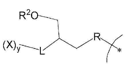
상기 화학식에서,
*은 화합물에 부착되는 부분이고,
y는 각각 1-2이며,
L은 각각 독립적으로 아미노, 에테르, 티오, 히드라진, 설피네이트, 설포네이트, 설폰아미드, 에스테르, 카르보네이트, 카르바메이트, 아미드, 또는 우레아 결합이고,
X는 각각 광 감쇠기, 용해 강화기, 접착 촉진기, 레올로지 개질제, 및 그의 조합으로 이루어진 군으로부터 선택되는 화학적 개질기이며, 상기 광 감쇠기는 벤젠, 나프탈렌, 안트라센, C1-C12 알킬, 및 그의 치환된 유도체로 이루어진 군으로부터 선택되고, 상기 용해 강화기는 히드록시 기, 산, 및 지방 사슬로 이루어진 군으로부터 선택되고, 상기 접착 촉진기는 알코올, 극성 기, 및 티올로 이루어진 군으로부터 선택되고, 상기 레올로지 개질제는 페놀 및 히드록실로 이루어진 군으로부터 선택되며,
R는 각각 독립적으로 -O- 또는 -CH2-이고,
R2는 각각 독립적으로 -H, 알킬, 설포네이트, 에스테르, 카르보네이트, 카르바메이트, 또는 그의 기능화된 유도체이다.A core component, and at least two epoxy residues and at least one adamantyl group, each bonded to the core component,
Wherein at least one of the epoxy moieties has the formula:
or
In the above formula,
* Is the part attached to the compound,
y is 1-2,
L is each independently amino, ether, thio, hydrazine, sulfinate, sulfonate, sulfonamide, ester, carbonate, carbamate, amide, or urea bond,
X is a chemical modifier selected from the group consisting of a light attenuator, a dissolution enhancer, an adhesion promoter, a rheology modifier, and a combination thereof, each of which is a benzene, naphthalene, anthracene, C 1 -C 12 alkyl, and substitutions thereof The dissolution enhancer is selected from the group consisting of hydroxy groups, acids, and fatty chains, the adhesion promoter is selected from the group consisting of alcohols, polar groups, and thiols, the rheology The modifier is selected from the group consisting of phenol and hydroxyl,
Each R is independently —O— or —CH 2 —,
Each R 2 is independently —H, alkyl, sulfonate, ester, carbonate, carbamate, or a functionalized derivative thereof.
상기 화학적 개질기는 히드록시기로 추가로 치환되는 것인 화합물.The method of claim 28,
Wherein said chemical modifier is further substituted with a hydroxy group.
상기 코어 구성요소는 방향족 또는 지방족 환형 화합물, 비환형(acyclic) 화합물, 및 그의 기능성 유도체로 이루어진 군으로부터 선택되는 것인, 화합물.The method of claim 28,
Wherein said core component is selected from the group consisting of aromatic or aliphatic cyclic compounds, acyclic compounds, and functional derivatives thereof.
상기 코어 구성요소는 벤젠, 시클로알칸, 헤테로시클, 분지형 또는 선형의 알킬, 알켄, 또는 알카인의 기능성 유도체인 것인 화합물.The method of claim 28,
Wherein said core component is a functional derivative of benzene, cycloalkane, heterocycle, branched or linear alkyl, alkene, or alkane.
상기 R은 -O-인 것인 화합물.The method of claim 28,
R is -O-.
상기 L은 에스테르 결합인 것인 화합물.The method of claim 28,
L is an ester bond.
상기 화합물은 500 내지 2,000 달톤(Dalton)의 중량 평균 분자량을 갖는 것인 화합물.The method of claim 28,
The compound has a weight average molecular weight of 500 to 2,000 Daltons (Dalton).
상기 화합물은 모노머 반복 단위가 없는 것인 화합물.The method of claim 28,
Wherein said compound is devoid of monomer repeat units.
상기 비폴리머성 화합물은 화학적 개질기와 전구체 화합물의 반응에 의해 형성되고,
상기 전구체 화합물은 하기 화학식으로 이루어진 군으로부터 선택되는 화합물:

및

상기 식에서
x는 각각 0-3이고, m은 각각 2 이상이며, n은 1 이상이고, R은 각각 독립적으로 -O- 또는 -CH2-이며, R’는 각각 독립적으로 할로겐 원자 또는 지방족 탄화수소이다.The method of claim 28,
The nonpolymeric compound is formed by the reaction of a chemical modifier with a precursor compound,
The precursor compound is a compound selected from the group consisting of:
And
In the above formula
x are each 0-3, m is at least 2, respectively, n is a, R are independently -O- or -CH 2 each is 1 or above, and, R 'are each independently a halogen atom or an aliphatic hydrocarbon.
상기 비폴리머성 화합물은 상기 에폭시 잔기 및 상기 아다만틸 기가 각각 결합되어 있는 코어 구성요소를 더 포함하는 방법.The method of claim 1,
Wherein said nonpolymeric compound further comprises a core component to which said epoxy moiety and said adamantyl group are each bound.
상기 코어 구성요소는 방향족 또는 지방족 환형 화합물, 비환형 화합물, 및 그의 기능성 유도체로 이루어진 군으로부터 선택되는 것인 방법.The method of claim 39,
Wherein said core component is selected from the group consisting of aromatic or aliphatic cyclic compounds, acyclic compounds, and functional derivatives thereof.
상기 코어 구성요소는 벤젠, 시클로알칸, 헤테로시클, 분지형 또는 선형의 알킬, 알켄, 또는 알카인의 기능성 유도체인 것인 방법.The method of claim 39,
Wherein said core component is a functional derivative of benzene, cycloalkane, heterocycle, branched or linear alkyl, alkene, or alkane.
상기 코어 구성요소는 방향족 또는 지방족 환형 화합물, 비환형 화합물, 및 그의 기능성 유도체로 이루어진 군으로부터 선택되는 것인 조성물.The method of claim 15,
Wherein said core component is selected from the group consisting of aromatic or aliphatic cyclic compounds, acyclic compounds, and functional derivatives thereof.
상기 코어 구성요소는 벤젠, 시클로알칸, 헤테로시클, 분지형 또는 선형의 알킬, 알켄, 또는 알카인의 기능성 유도체인 것인 조성물.The method of claim 15,
Wherein said core component is a functional derivative of benzene, cycloalkane, heterocycle, branched or linear alkyl, alkene, or alkane.
상기 비폴리머성 화합물은 상기 에폭시 잔기 및 상기 아다만틸 기가 각각 결합되어 있는 코어 구성요소를 더 포함하는 구조물.The method of claim 19,
The nonpolymeric compound further comprises a core component to which the epoxy moiety and the adamantyl group are each bonded.
상기 코어 구성요소는 방향족 또는 지방족 환형 화합물, 비환형 화합물, 및 그의 기능성 유도체로 이루어진 군으로부터 선택되는 것인 구조물.The method of claim 44,
Wherein said core component is selected from the group consisting of aromatic or aliphatic cyclic compounds, acyclic compounds, and functional derivatives thereof.
상기 코어 구성요소는 벤젠, 시클로알칸, 헤테로시클, 분지형 또는 선형의 알킬, 알켄, 또는 알카인의 기능성 유도체인 것인 구조물.The method of claim 44,
Wherein said core component is a functional derivative of benzene, cycloalkane, heterocycle, branched or linear alkyl, alkene, or alkane.
R2는 각각 독립적으로 -H, 알킬, S(O)2X, (C=O)X, (C=O)OX, (C=O)N(X1X2), 또는 그의 기능화된 유도체이고,
X, X1 및 X2는 독립적으로 광 감쇠기, 용해 강화기, 접착 촉진기, 레올로지 개질제, 및 그의 조합으로 이루어진 군으로부터 선택되며, 상기 광 감쇠기는 벤젠, 나프탈렌, 안트라센, C1-C12 알킬, 및 그의 치환된 유도체로 이루어진 군으로부터 선택되고, 상기 용해 강화기는 히드록시 기, 산, 및 지방 사슬로 이루어진 군으로부터 선택되고, 상기 접착 촉진기는 알코올, 극성 기, 및 티올로 이루어진 군으로부터 선택되고, 상기 레올로지 개질제는 페놀 및 히드록실로 이루어진 군으로부터 선택되는 것인 조성물.The method of claim 11,
Each R 2 is independently —H, alkyl, S (O) 2 X, (C═O) X, (C═O) OX, (C═O) N (X 1 X 2 ), or a functionalized derivative thereof ego,
X, X 1 and X 2 are independently selected from the group consisting of light attenuators, dissolution enhancers, adhesion promoters, rheology modifiers, and combinations thereof, wherein the light attenuators are benzene, naphthalene, anthracene, C 1 -C 12 alkyl And a dissolution enhancer is selected from the group consisting of hydroxy groups, acids, and fatty chains, and the adhesion promoter is selected from the group consisting of alcohols, polar groups, and thiols; , Wherein the rheology modifier is selected from the group consisting of phenol and hydroxyl.
193 nm 또는 248 nm의 파장에서 1.3 내지 2의 n 값을 갖는 층을 형성하도록 경화될 수 있는 것인 조성물.The method of claim 11,
The composition can be cured to form a layer having an n value of 1.3 to 2 at a wavelength of 193 nm or 248 nm.
0.01 내지 0.8의 k 값을 갖는 층을 형성하도록 경화될 수 있는 것인 조성물.The method of claim 11,
The composition can be cured to form a layer having a k value of 0.01 to 0.8.
Applications Claiming Priority (3)
| Application Number | Priority Date | Filing Date | Title |
|---|---|---|---|
| US201261588268P | 2012-01-19 | 2012-01-19 | |
| US61/588,268 | 2012-01-19 | ||
| PCT/US2013/021932 WO2013109748A1 (en) | 2012-01-19 | 2013-01-17 | Nonpolymeric antireflection compositions containing adamantyl groups |
Publications (2)
| Publication Number | Publication Date |
|---|---|
| KR20150034122A KR20150034122A (en) | 2015-04-02 |
| KR102017360B1 true KR102017360B1 (en) | 2019-09-02 |
Family
ID=48796396
Family Applications (1)
| Application Number | Title | Priority Date | Filing Date |
|---|---|---|---|
| KR1020147021741A KR102017360B1 (en) | 2012-01-19 | 2013-01-17 | Nonpolymeric antireflection compositions containing adamantyl groups |
Country Status (8)
| Country | Link |
|---|---|
| US (1) | US9328246B2 (en) |
| EP (1) | EP2805347B1 (en) |
| JP (1) | JP6410256B2 (en) |
| KR (1) | KR102017360B1 (en) |
| CN (1) | CN104137235B (en) |
| SG (1) | SG11201404229YA (en) |
| TW (1) | TWI587094B (en) |
| WO (1) | WO2013109748A1 (en) |
Families Citing this family (9)
| Publication number | Priority date | Publication date | Assignee | Title |
|---|---|---|---|---|
| JP6449145B2 (en) | 2012-04-23 | 2019-01-09 | ブルーワー サイエンス アイ エヌ シー. | Photosensitive, developer-soluble bottom antireflection film material |
| CN104701238B (en) * | 2013-11-14 | 2019-10-08 | 罗门哈斯电子材料有限公司 | Gap filling method |
| CN106384719B (en) * | 2015-08-06 | 2020-06-23 | 王贝贝 | Processing method for etching black phosphorus two-dimensional material body by using oxygen plasma |
| TWI662370B (en) | 2015-11-30 | 2019-06-11 | 南韓商羅門哈斯電子材料韓國公司 | Coating compositions for use with an overcoated photoresist |
| US10079152B1 (en) * | 2017-02-24 | 2018-09-18 | Canon Kabushiki Kaisha | Method for forming planarized etch mask structures over existing topography |
| WO2019014465A1 (en) * | 2017-07-14 | 2019-01-17 | Glisten Llc | Gemstone coatings and methods of making and using the same |
| US10604618B2 (en) | 2018-06-20 | 2020-03-31 | Shin-Etsu Chemical Co., Ltd. | Compound, method for manufacturing the compound, and composition for forming organic film |
| EP3911197A4 (en) * | 2019-01-14 | 2022-03-09 | Glisten LLC | Molecular coatings and methods of making and using the same |
| KR20230148608A (en) * | 2022-04-18 | 2023-10-25 | 한남대학교 산학협력단 | Surface modified metal oxide and ink composition comprising the same |
Citations (2)
| Publication number | Priority date | Publication date | Assignee | Title |
|---|---|---|---|---|
| JP2005263264A (en) | 2004-03-18 | 2005-09-29 | Tokyo Ohka Kogyo Co Ltd | Container for photoresist composition |
| WO2011125326A1 (en) | 2010-04-07 | 2011-10-13 | 三菱瓦斯化学株式会社 | Method for purifying alkylnaphthalene formaldehyde polymer |
Family Cites Families (26)
| Publication number | Priority date | Publication date | Assignee | Title |
|---|---|---|---|---|
| US5858618A (en) * | 1996-12-02 | 1999-01-12 | Nan Ya Plastics Corporation | Photopolymerizable resinous composition |
| US7323289B2 (en) * | 2002-10-08 | 2008-01-29 | Brewer Science Inc. | Bottom anti-reflective coatings derived from small core molecules with multiple epoxy moieties |
| TW200519081A (en) * | 2003-10-03 | 2005-06-16 | Nagase Chemtex Corp | An alkali soluble resin |
| JP4665189B2 (en) * | 2003-10-03 | 2011-04-06 | ナガセケムテックス株式会社 | Alkali-soluble resin |
| JP4769455B2 (en) * | 2003-12-30 | 2011-09-07 | ローム・アンド・ハース・エレクトロニック・マテリアルズ,エル.エル.シー. | Coating composition |
| JP4491283B2 (en) | 2004-06-10 | 2010-06-30 | 信越化学工業株式会社 | Pattern formation method using antireflection film-forming composition |
| JP4421566B2 (en) * | 2005-12-26 | 2010-02-24 | チェイル インダストリーズ インコーポレイテッド | Hard mask composition for photoresist underlayer film and method of manufacturing semiconductor integrated circuit device using the same |
| CN101370797B (en) * | 2006-01-27 | 2012-04-11 | 出光兴产株式会社 | Adamantane derivative, resin composition containing the derivative, and optical electronic component and electronic circuit sealing agent using the same |
| WO2007094173A1 (en) * | 2006-02-17 | 2007-08-23 | Idemitsu Kosan Co., Ltd. | Adamantane derivative, composition comprising the derivative, and optical and electronic member using the composition |
| KR101388703B1 (en) | 2006-04-28 | 2014-04-24 | 이데미쓰 고산 가부시키가이샤 | Adamantyl group-containing epoxy-modified (meth)acrylate and resin composition containing the same |
| US20090099326A1 (en) * | 2006-04-28 | 2009-04-16 | Idemitsu Kosan Co., Ltd. | Fluorine-containing adamantane derivative, fluorine-containing adamantane derivative having polymerizable group, resin composition containing the same, and antireflection film |
| JP5134233B2 (en) * | 2006-11-29 | 2013-01-30 | 出光興産株式会社 | ADAMANTAN DERIVATIVE, PROCESS FOR PRODUCING THE SAME AND RESIN COMPOSITION CONTAINING ADAMANTAN DERIVATIVE |
| CN101548203B (en) * | 2007-06-11 | 2012-03-07 | 三菱化学株式会社 | Photosensitive color resin composition for color filter, color filter, liquid crystal display, and organic el display |
| JP5337983B2 (en) * | 2007-09-19 | 2013-11-06 | 日産化学工業株式会社 | Lithographic resist underlayer film forming composition comprising a polymer having a polycyclic aliphatic ring |
| JP5122229B2 (en) * | 2007-09-28 | 2013-01-16 | クラレノリタケデンタル株式会社 | Polymerizable adamantane derivative and dental composition |
| DE112009000979B4 (en) * | 2008-04-23 | 2014-12-11 | Brewer Science, Inc. | Photosensitive hardmask for microlithography |
| US7932018B2 (en) * | 2008-05-06 | 2011-04-26 | Az Electronic Materials Usa Corp. | Antireflective coating composition |
| US20100040838A1 (en) * | 2008-08-15 | 2010-02-18 | Abdallah David J | Hardmask Process for Forming a Reverse Tone Image |
| JP2010186174A (en) * | 2009-01-16 | 2010-08-26 | Mitsubishi Chemicals Corp | Method for manufacturing color filter, color filter, and use thereof |
| WO2010096615A2 (en) | 2009-02-19 | 2010-08-26 | Brewer Science Inc. | Acid-sensitive, developer-soluble bottom anti-reflective coatings |
| JP2010224158A (en) * | 2009-03-23 | 2010-10-07 | Idemitsu Kosan Co Ltd | Composition containg (meth)acrylate compound and photosensitive resin laminate formed by using the same |
| JP5229044B2 (en) * | 2009-03-26 | 2013-07-03 | Jsr株式会社 | Resist underlayer film forming composition, resist underlayer film, resist underlayer film forming method, and pattern forming method |
| JP2010250180A (en) * | 2009-04-17 | 2010-11-04 | Idemitsu Kosan Co Ltd | Photosensitive composition containing adamantane derivative |
| JP5352340B2 (en) * | 2009-05-13 | 2013-11-27 | 株式会社タムラ製作所 | Photosensitive resin composition, solder resist composition for printed wiring board, and printed wiring board |
| CN102311346B (en) * | 2011-06-20 | 2014-06-25 | 常州大学 | Adamantane-containing resin as well as preparation method and application thereof |
| JP6449145B2 (en) * | 2012-04-23 | 2019-01-09 | ブルーワー サイエンス アイ エヌ シー. | Photosensitive, developer-soluble bottom antireflection film material |
-
2013
- 2013-01-17 KR KR1020147021741A patent/KR102017360B1/en active IP Right Grant
- 2013-01-17 WO PCT/US2013/021932 patent/WO2013109748A1/en active Application Filing
- 2013-01-17 JP JP2014553407A patent/JP6410256B2/en active Active
- 2013-01-17 SG SG11201404229YA patent/SG11201404229YA/en unknown
- 2013-01-17 CN CN201380010902.7A patent/CN104137235B/en active Active
- 2013-01-17 US US13/743,965 patent/US9328246B2/en active Active
- 2013-01-17 EP EP13738476.4A patent/EP2805347B1/en active Active
- 2013-01-18 TW TW102102173A patent/TWI587094B/en active
Patent Citations (2)
| Publication number | Priority date | Publication date | Assignee | Title |
|---|---|---|---|---|
| JP2005263264A (en) | 2004-03-18 | 2005-09-29 | Tokyo Ohka Kogyo Co Ltd | Container for photoresist composition |
| WO2011125326A1 (en) | 2010-04-07 | 2011-10-13 | 三菱瓦斯化学株式会社 | Method for purifying alkylnaphthalene formaldehyde polymer |
Also Published As
| Publication number | Publication date |
|---|---|
| US9328246B2 (en) | 2016-05-03 |
| SG11201404229YA (en) | 2014-08-28 |
| JP6410256B2 (en) | 2018-10-24 |
| CN104137235A (en) | 2014-11-05 |
| EP2805347A4 (en) | 2015-07-22 |
| US20130186851A1 (en) | 2013-07-25 |
| EP2805347A1 (en) | 2014-11-26 |
| KR20150034122A (en) | 2015-04-02 |
| EP2805347B1 (en) | 2018-03-07 |
| TWI587094B (en) | 2017-06-11 |
| JP2015507223A (en) | 2015-03-05 |
| WO2013109748A1 (en) | 2013-07-25 |
| CN104137235B (en) | 2017-02-22 |
| TW201344370A (en) | 2013-11-01 |
Similar Documents
| Publication | Publication Date | Title |
|---|---|---|
| KR102017360B1 (en) | Nonpolymeric antireflection compositions containing adamantyl groups | |
| JP6592243B2 (en) | Assist layer for EUV lithography | |
| KR100896451B1 (en) | HIGH ETCH RESISTANT HARDMASK COMPOSITION HAVING ANTIREFLECTIVE PROPERTY?WITH IMPROVEMENT OF CARBON CONTENTS?and Process of producing patterned materials by using the same | |
| TWI440972B (en) | Method of creating photolithographic structures with developer-trimmed hard mask | |
| JP4852360B2 (en) | Method for forming a base layer composition, lithographic structure, material layer or material element comprising a heterocyclic aromatic structure used in a multilayer lithography process on a substrate | |
| JP2010529499A (en) | Anti-reflective hard mask composition and method for patterning material on a substrate using the same | |
| JP2007178974A (en) | Hard mask composition for photoresist underlayer film and method for producing semiconductor integrated circuit device using same | |
| WO2008082236A1 (en) | Polymer having antireflective properties, hardmask composition including the same, and process for forming a patterned material layer | |
| JP2007258683A (en) | Hardmask composition for resist underlayer film including organosilane polymer and method of manufacturing semiconductor integrated circuit device using the same | |
| TW201500859A (en) | A composition comprising a polymeric thermal acid generator and processes thereof | |
| TWI411628B (en) | Underlayer composition having anti-reflective property | |
| KR100844019B1 (en) | HIGH ETCH RESISTANT HARDMASK COMPOSITION HAVING ANTIREFLECTIVE PROPERTY WITH IMPROVEMENT OF CARBON CONTENTS and Process of producing patterned materials by using the same | |
| KR100713231B1 (en) | Hardmask composition coated under photoresist and process of producing integrated circuit devices using thereof | |
| KR20070095736A (en) | Hardmask composition coated under photoresist comprising organosilane polymer and process of producing integrated circuit devices using thereof | |
| KR100725793B1 (en) | Hardmask composition coated under photoresist and process of producing integrated circuit devices using thereof | |
| TW201229693A (en) | Gap embedding composition, method of embedding gap and method of producing semiconductor device by using the composition | |
| KR100725794B1 (en) | Hardmask composition coated under photoresist and process of producing integrated circuit devices using thereof | |
| KR100783064B1 (en) | Organosilane composition, Hardmask Composition Coated under Photoresist and Process of producing integrated circuit devices using thereof | |
| KR100725795B1 (en) | Hardmask composition coated under photoresist and process of producing integrated circuit devices using thereof | |
| WO2008075860A1 (en) | High etch resistant hardmask composition having antireflective properties, method for forming patterned material layer using the hardmask composition and semiconductor integrated circuit device produced using the method | |
| KR100713238B1 (en) | Hardmask composition coated under photoresist and process of producing integrated circuit devices using thereof | |
| KR20110077684A (en) | Polymer for under-layer of resist, under-layer composition of resist, method of patterning device using same | |
| KR20100130417A (en) | Dendritic compound for hardmask and composition for hardmask comprising the same | |
| JP2024008372A (en) | Composition for forming metal oxide film, method for forming pattern, and method for forming metal oxide film | |
| KR100783070B1 (en) | Organosilane composition, Hardmask Composition Coated under Photoresist and Process of producing integrated circuit devices using thereof |
Legal Events
| Date | Code | Title | Description |
|---|---|---|---|
| A201 | Request for examination | ||
| E902 | Notification of reason for refusal | ||
| E701 | Decision to grant or registration of patent right | ||
| GRNT | Written decision to grant |